reduce the design area. The transmission gate also reduces the number of stray capacitances will improve speed and power dissipation of design. The shift registers are design using edge triggered flip flops but the use of latches for shift register design also optimizes the area. For this design a non overlap clock pulses are used. This solves the timing problem between pulsed latches through the use of multiple non-overlap delayed pulsed clock signals instead of the conventional single pulsed clock signal. The shift register uses a small number of the pulsed clock signals by grouping the latches to several sub shifter registers and using additional temporary storage latches.
Key words:-
Pulse latch, Shift Register, CMOS design,I.
INTRODUCTION
The shift registers are commonly used for memory designs. The shift registers are design using edge triggered flip flops. All the flip flops are synchronized through clock signals. The increase in word length of shift register will increase the number of flip flops. The edge triggered flip flops are design with two or more than two latches. The general structure of flip flop is design using master slave latches. The internal structure of shift register composed of N number of series connected D flip flops. The latches are design using combination multiplexer logic cell using transmission gates. The structure of N bit shift register is composed of series connected synchronized N number of flip flops. The shift register is design with cascaded flip flops hence there is no interconnected circuits between the flip flops hence speed is not the major constraints of shift register design as compare to area and power. The latches are mostly not used in design of shift register ue to its timing problems. The non overlap pulse latches are the better option of design of shift registers. It reduces the number of transistors for design which in turn also reduces the area and power consumption.
II.
PULSE CLOCK GENERATOR
Figure1: Schematic Diagram for pulse clock generator
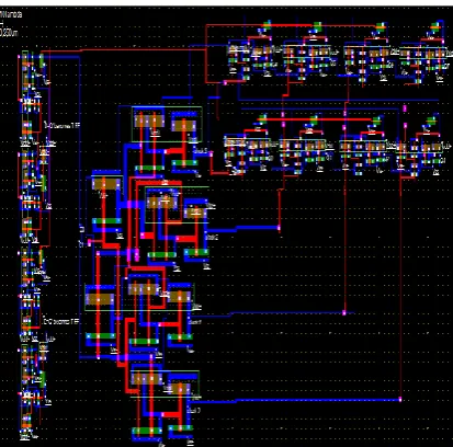
Figure2: CMOSLayout Design for clock pulse generator
Fig 2 shows the CMOS layout design for clock pulse generator. The design is composed of two bit counter and a 2:4 decoder circuit. The decoder circuit generates the four clock pulses of finite time duration which can be further use for pulse clock signals of shift registers latches.
connected to the input terminal of latch0. The pulse clock generator circuit activates any one of its output clock port. Thus one pulse latch responds to its input terminal at every clock edge of clock pulse generator circuit. Thus data is shifted to its successive latch synchronously.
Figure4: Schematic Diagram for 4 bit pulse latch base shift register.
Eight Bit Pulse latch Shift Register: The fig 5 shows the 8 bit pulse latch shift register. It includes 8 latch circuits whose clock signal is connected through pulse clock generator circuit. Clk0 is connected to latch 0 and latch1, clk1 is connected to latch2 and latch3, clk2 is connected to latch4 and latch5 and clk3 is connected to latch 6 and latch 7 respectively.
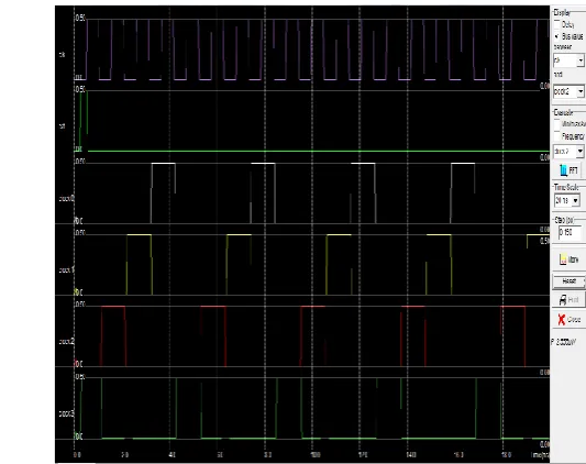
Figure 6: Timing Simulation for 4 bit pulse latch shift register
The timing simulation of 8 bit pulse latch shift register shows the data at input terminal Din is shifted with the arrival of every non overlap clock pulses. The non overlap pulse clock will activates only one latch at a time and the data available at its input terminal is shifted towards the output terminal of that latch.
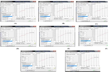
Figure 7:Graphical Analysis of power dissipation at output (A) node Q0 (B) node Q1 (C) Nodes Q2 (D)node Q3 (E ) node Q4 (F) node Q5 (G) node Q6 (H) node Q7.
Table I: Comparative Analysis
Type [1] This Work
Transistor Size (μm/μm) NMOS 0.5/1.8
PMOS 0.5/1.8
NMOS 0.05/0.1 PMOS 0.05/0.15
Latch area 19.2 μm2
(6.7μmX5.6μm)
2.8125μm2 (2.25μmX1.25μm)
Latch Power Dissipation 3.30 μW 0.209μW
Number of Transistors in Latch 7 10
Transactions On Circuits And Systems—I: Regular Papers, Vol. 62, No. 6, June 2015 pp no 1564. [2]. Masaki Masuda, Kanto Kubota, Ryosuke Yamamoto, Jun Furuta, Kazutoshi Kobayashi, and Hidetoshi
Onodera "A 65 nm Low-Power Adaptive-Coupling Redundant Flip-Flop" IEEE Transactions On Nuclear Science, Vol. 60, No. 4, August 2013 pp no 2750.
[3]. K. Kobayashi, K. Kubota, M. Masuda, Y. Manzawa, J. Furuta, S. Kanda, and H. Onodera "A Low-Power and Area-Efficient Radiation-Hard Redundant Flip-Flop, DICE ACFF, in a 65 nm Thin-BOX FD-SOI" IEEE Transactions On Nuclear Science, Vol. 61, No. 4, August 2014 pp no. 1881.
[4]. A.ParvathiKarthica "Power Efficient Synchronous Counter Using Transmission-Gate Based Master-Slave Flip-Flop With Modified Logical Effort Optimization" International Conference on Electronics and Communication Engineering (ECE) 7th April 2013 ppno. 86.
[5]. S. EhsanRazavi, " Shift Register Design Using D-Flip flop with Low Power Consumption and High Speed " International Journal of Science and Advanced Technology (ISSN 2221-8386) Volume 1 No 7 September 2011