Preparation of BST Capacitors Using sol-gel Process
for Distance Sensor
RAHMI DEWI
1*, KRISMAN
1, SUGIANTO
1, ZUHDI
2, N.B. IBRAHIM
31Physics Dept, Math and Science Faculty, Universitas Riau, Pekanbaru, 28293, Indonesia
2Faculty of Teacher Training and Education, Universitas Riau, Pekanbaru, 28293, Indonesia
3School of Applied Physics, Faculty of Science and Technology, Universiti Kebangsaan Malaysia, 43600, Bangi, Selangor, Malaysia.
*Email of corresponding author: [email protected]
Abstract--Barium strontium titanate (Ba1-xSrxTiO3) thin films prepared to BST/TiO2/RuO2/SiO2/Si substrates using sol-gel process with composition x = 0.4. Then the sample annealed at 600oC, 650oC and 700°C for 60 minutes in the air. The XRD pattern, dielectric properties and leakage current films have been measured to investigate the effect of annealing temperature on the properties of the device. The results showed that all the films have a perovskite structure. Dielectric measurements show that at 25oC and 1 kHz, the dielectric constant and loss tangent of about 67 and 2.07; 341 and 3.23; 1300 and 0.54, respectively. Leakage current to 0.5 V at room temperature is 8.23 x 10⁻⁵ A cm-2, 2.77 x 10⁻⁵ A cm-2 and 2.00 x 10⁻⁴ A cm-2, respectively. The highest voltage value at a distance of 5 cm was obtained for the sensor.
Index Term--Barium Strontium Titanate; sol-gel process; distance sensor
INTRODUCTION
Infrared sensor distance is almost exclusively used as a detector close to the mobile robot. It offers lower costs and a faster response time of an ultrasonic distance sensor [1]. Recently, much attention has been focused on the infrared thermal images can be obtained easily without refrigeration sensing pixels and there is a great potential in the commercial market [2]. Ba1-xSrxTiO3 (BST) today is one of the most interesting ferroelectric material for the high dielectric constant and depends on the composition of the Curie temperature. At room temperature is a ferroelectric BST when the Ba content x is in the range from 0.3 to 0 and paraelectric when x is in the range of 0.3-1 [3]. This process is most important is how to store the ferroelectric thin film as the sensitivity of the sensor is directly derived from BST thin film properties. In our previous work, all BST thin films prepared by sol-gel method. Which has advantages compared to other methods of control of homogeneity, cost and process [4].
In this paper we report the preparation of dielectric properties and leakage current Ba0.6Sr0.4TiO3 thin film made by sol-gel method. Micro, dielectric properties and leakage current film annealed at different temperatures for example 600oC, 650oC and 700°C for 60 minutes, investigated and dealt with the application as a proximity sensor. The proximity sensor is very important in a mobile robot. BST is a metal oxide material with a high dielectric constant, high strength fraction, the dielectric loss is small, and good thermal stability.
In particular, the BST thin film is considered one of the most promising dielectric materials for high density capacitors in DRAM. Important parameters that describe the stages of sensor sensitivity is the change output voltage (ΔV). The resulting voltage value is higher compared with those produced by other researchers, this is due grain sizes in the nanometer size.
The dielectric constant for some very useful dielectric changes as a function of electric field is used, for example, ferroelectric materials, so the capacitance of these devices is more complex. For example, in charging such as capacitors increase in the voltage differential to charges apply:
(1)
where the voltage dependence of capacitance, C (V), shows that the capacitance is a function of electric field strength, which in the large area parallel plate is given by d ε = V /. This field polarizes the dielectric, polarized, in the case of ferroelectric, is a linear function of the S-shaped electric field, which, in the case of a large area parallel plate device, is translated into linear capacitance is a function of voltage. Parallel to capacitance voltage depending on, for charging the capacitor voltage V related important available:
(2)
in where agreed with Q = CV only when C does not depend on the voltage V. By the same taken, the energy stored in the capacitor is now given by
(3)
Integrating:
(4)
semiconductor diodes, in which the voltage dependence that is not derived from the change in the dielectric constant but the voltage dependence of the distance between the charge on both sides of the capacitor. This effect is deliberately exploited in devices like diodes known as varicaps.
Depending on the frequency capacitors
If the capacitor is driven by a voltage change with time that changed quite rapidly, at a frequency dielectric polarization can not follow voltage. For example, the origin of this mechanism, polished internal microscopic contribute dielectric constant can not move at all, and so the frequency of the applied voltage increases Shuttle, dipole response is limited and reduced dielectric constant. The dielectric constant change with frequency is called as dielectric dispersion, and be governed by the dielectric relaxation process, such as the Debye relaxation. In the transient state, the displacement can be expressed as a tendency electricity:
( 5 ) Showing lag as a response by the time dependence of εr, calculated essentially on the basis of microscopic analysis, for example, the behavior of the dielectric dipole. See, for example, linear response function. Integral power over the entire history of the past to the present. A later incarnation Time Fourier cause:
(6)
where εr (ω) is now a complex function, the imaginary part related to the absorption of energy from the field to the medium. See transparency. Capacitance, which is in line with the dielectric constant, also shows the behavior of this frequency. Fourier transform Gauss 'law' s with this form to the terrain shifts:
(7)
where j is the imaginary unit, V (ω) is a component of the voltage at the angular frequency ω, G (ω) is the real part of the time, called conductance, and C (ω) determines the imaginary part time, and capacitance. Z (ω) is the complex impedance. When a parallel-plate capacitor filled with dielectric, a simple measurement of dielectric properties is based on the relationship:
(8) where a single prime mark the real part and the prime twice that delusion, Z (ω) is the complex impedance with the present dielectric, Ccomplx (ω) is the complex capacitance socalled with the present dielectric, and Co is the capacitance without the dielectric. (Measurements "without dielectric" basically
means the size of the free space, a goal that can not be achieved because although the quantum vacuum is expected to behave is not good, as dischroism. For practical purposes, when the measurement errors are taken into account, usually the size of the vacuum mainland, or simply the calculation of Co, is quite appropriate. Using this measurement method, the dielectric constant can show resonances at certain frequencies related to the frequency response of the features (excitation energy) contributor to the dielectric constant. This resonance is the basis for some of the experimental technique for defect detection. The measures the absorption method as a function of frequency. in addition, the response time of the capacitance that can be used directly, as in the phase spectroscopy mortal, yet another example of frequency capacitance depends happened with the MOS capacitor, where generations slowly minority carrier means at high frequency capacitance steps just welcome the majority carriers, while in the low frequency carrier both types of reactions. At optical frequencies, in the semiconductor structure exhibits dielectric constant associated with the structure of the solid lines. Sophisticated methods of measurement of modulation spectroscopy based modulator crystal structure by pressure or other pressure, and observe the related changes in the absorption or reflection of light has advanced our knowledge of these materials. From the data obtained are conductance and dielectric constant εr of the films were calculated using formula:
A
d
C
o r.
.
( 9 )A
Z
d
.
(10)where d is the thickness, Z is the impedance, C is capacitance, εo is the vacuum permittivity, σ is the conductance and A is the area.
EXPERIMENTAL METHOD
air for 60 minutes. To measure the dielectric properties of BST thin films, metal-insulator-metal (MIM) structure has been engineered. The RuO2 bottom layer (~ 100 nm) and TiO2 insulating layer (~ 70 nm) were successively stored at 500oC
on a substrate via e-gun evaporation. A hard mask was placed over the substrate and the thin BST films deposited using a sol-gel process. Then Al electrode (~ 70 nm) deposited onto the film. Capacitor structure shown in Figure 1.
Fig. 1. The thin film capacitor structure
Crystal orientation, dielectric properties and leakage when the film was examined using a model X-ray diffractometer (XRD) Braker D8 Advance, impedance spectroscopy 1255 models Solartron-Schlumberger and electrometer Model KEITHLEY, respectively. The grain size and the film thickness was measured using a model scanning electron microscope (SEM) LEO VPSEM 1450.
Schematic experimental set-up shown in Figure 2. The system's infrared proximity sensor. infrared light from the LED with a peak wavelength at 830 nm are illuminated on the detecting capacitor, CBST through the tube and the infrared
lens. CBST has been connected to the circuit with a supply voltage of 1.8 volts. LED Driver (model 505B NEWPORT diode laser guidance) has been switched to the generator to function as player beheaded. In that case, the helicopter was only used to see a change in the DC output level between with and without infrared radiation. Illuminated infrared radiation to the device at a distance of 5 cm to 80 cm. Detector device has been set in an iron box-shielding to reduce noise. Final output signal was observed with an oscilloscope (Hitachi VC-6545 digital storage oscilloscope).
Fig. 2. System for IR distance sensor.
RESULT AND DISCUSS
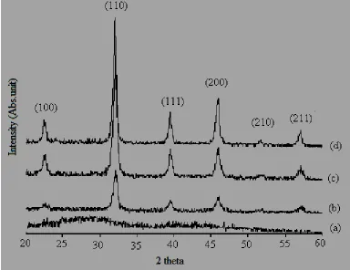
X-ray patterns diffraction films such willing and annealing shown in Fig. 3. Film as-supplied is amorphous and obscure films plated at 600oC and above is polycrystal. In general intensity and the sharpness of the peaks increases as the temperature increases annealing. In thin BST film, high-temperature annealing they needed to be true, it is caused by obstruction power between perovskite phase and the mid
Fig. 3. The XRD pattern of (a) Ba0.6Sr0.4TiO3 / SiO2 thin films as-prepared and after annealed at (b) 600oC (c) 650oC and (d) 700oC for 1 hours.
Table I shows a summary of the size and thickness of the film cereals were measured using SEM. All films have cereal nanometer size. Cereals size increases if the annealing temperature increases. This decision may be due to more defects annealed as the temperature increases and also a small
cereal combine to form larger grains. Increasing the size of the cereal also cause an increase in the film thickness as shown in Table 1. The dielectric constant thin films Ba0.6Sr0.4TiO3 measured using impedance analysts. Measurements were made at room temperature (25oC).
Table I
The average grain sizes and thick of BST films.
Annealing Temp. oC Average grain size (nm) Thickness (nm)
600 650 700
31.9 37.1 43.6
136.2 193.5 428.0
Fig. 4 shows frequency dependence of the dielectric constant (εr). In general, the dielectric constant decreases with increasing frequency. This shows that the polarization interface gradually weakened or lost with increasing frequency. Clearly it can also be seen from Fig.4 that the dielectric constant increases as the annealing temperature increases. This may be due to two factors. The first increase is in the film thickness as shown in Table 1 and the second
Fig. 4.The Frequency dependence of dielectric constant (εr) for BST thin films.
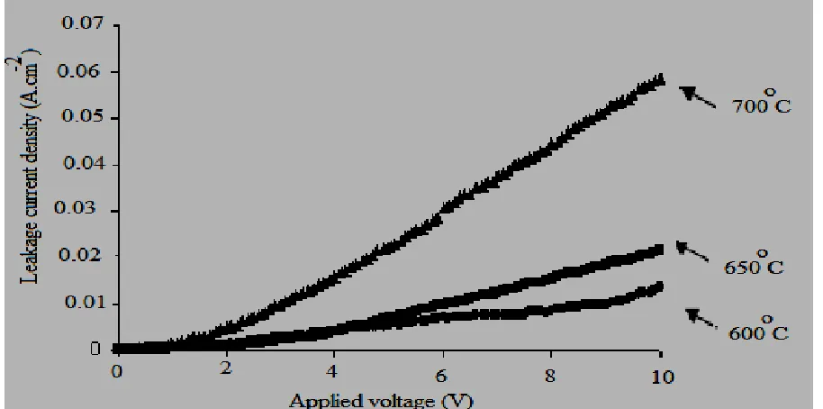
Graph leakage current density compared to the applied voltage is measured at room temperature (25oC) shown in Fig.5. Leakage current density for BST films plated shade at 600oC, 650oC and 700°C for 1 h at 0.5 V is 8.23 x 10⁻⁵ A/cm2, 2.77 x 10⁻⁵A/cm2 and 2.00 x 10⁻⁴A/cm2 respectively. BST leakage current density increased with the increase of annealing
temperature. Chiu et al. (2005) and Hwang et al. (2001) have reported similar results. Chiu et al. (2005) have reported, he knows that in the capacitor leakage current density metal/insulation/metal mainly due to transportation costs from metal electrodes or BST films throughout the interface (Schottky barrier) [8].
Fig. 5.Variation of leakage current density versus the applied voltage for BST films deposited at annealed at 600oC, 650oC and 700oC for 1 hours
Proximity sensor built structures on
Si/SiO2/RuO2/TiO2/BST/Al substrate with Ba0.6Sr0.4TiO3 formula under different annealing temperature is 600, 650 and 700°C. All sensor declared then tested the performance of sensitivity and repeatability aspects. Guo et al. (2004) [9], Kumar And Manavalan (2005) [10] and Xu et al. (2000) [11] have shown that the influence of grain size and thickness of the film of sustainable BST dielectric thin film using the main
respectively. Sensor plated at 600oC shade better than the gilded sensor device may be obscure at 650oC current flowing in at 600oC is the low yield of the barriers wearing very high. This sensor measurement results better than those made by Cheng et al. (2000), BST sensor with composition
Ba0.8Sr0.2TiO3 were made using sol-gel process and in annealing at a temperature of 750oC for 10 minutes, the measurement of the effect infrared absorption to the maximum output voltage at a frequency of 6 Hz is 3.2 mV [12].
Fig. 6. The voltage change versus distance for the BST films deposited at annealed at 600oC, 650oC and 700oC for 1 hours.
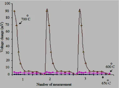
Figure 7 shows a sensor replicates the composition x = 0.4 annealed at temperatures of 700, 650 and 600oC. Found that repetition sensor annealed at 700°C was better than annealed
at 650 and 600oC. Recurrence occurred with almost the same sensitivity or sensor output voltage each time a measurement is repeated.
CONCLUSIONS
Proximity sensor built structures on
Si/SiO2/RuO2/TiO2/BST/Al substrate with formula Ba0.6Sr0.4TiO3 films have been successfully supplied by sol-gel method. This sensor can be used as a proximity sensor for a distance of between 5 cm to 80 cm. Sensor annealed at 700°C with 90.1 ± 3.2 mV readings better than the sensor annealed at 650oC and 600oC. In general, an increase in the annealing temperature increases polycrystalline films, the grain size, dielectric constant and leakage current of film.
ACKNOWLEDGMENT
Author would like to thank to supervisors and members of thin film group at Universiti Kebangsaan Malaysia for their advice and help.
REFERENCES
[1] G. Benet, F. Blanes, J.E. Simo, P. Perez, “Using infrared sensors for distance measurement in mobile robots,” Robotics and Autonomous Systems, vol. 40, pp. 255-266, 2002.
[2] M.Y. Fan, L. F. Zhang. "BST Nano-Powder for Infrared Detector Prepared by Sol-Gel Method",Applied Mechanics and Materials
vol. 364, pp 760-764, August. 2013.
[3] H. Zhu, H. Xu, M. Noda, T. Mukaigawa, K. Hashimoto, M. Okuyama,
“
Preparation of BST ferroelectric thin film by metal organic decomposition for infrared sensor” T. IEE vol. 121-E, pp. 308-312, 2001[4] D. Wu, A. Li, H. Ling, X. Yin, C. Ge, M. Wang, N. Ming, “Preparation of (Ba0.5Sr0.5)TiO3 thin films by sol–gel method with rapid thermal annealing” .Appl. Surface Sci. vol. 165, pp.309-314 , 2000
[5] S. Ezhilvalavan & T.Y. Tseng, “Progress in the developments of (Ba,Sr)TiO3 (BST) thin films for gigabit era DRAMs,” Mater.
Chem. and Phys. Vol. 65, pp. 227-248, 2000.
[6] H.Y. Tian,W.G. Luo, A.L. Ding, J. Choi, C. Lee, K. No, “Influences of annealing temperature on the optical and structural preoperties of (Ba,Sr)TiO3 thin films derived from sol-gel technique,”Thin Solid Films vol. 408, pp. 200-205, 2002 [7] C.M. Chu & P. Lin, “Electrical properties and crystal structures of
(Ba,Sr)TiO3 films and BaRuO3 bottom electrodes prepared by sputtering,”Appl.Phys.Lett vol.72, .pp. 1241- 1243, 1998. [8] M.C.Chiu, C.C. Wang, H.C. Yao, F.S. Shieu, “Microstructure and
electrical properties of Ba1 − xSrxTiO3 thin films prepared by rf magnetron sputtering,” Materials Chemistry and Physics vol.
94(1), pp 141-147, Nov. 2005
[9] H. Guo, W. Gao, J. Yoo, “The effect of sintering on the properties of Ba0.7Sr0.3TiO3 ferroelectric films produced by electrophoretic deposition,”J. Materials Letters 58, pp.1387-1391, 2004
[10] A.Kumar & S.G. Manavalan,
“
Characterization of barium strontium titanate thin films for tunable microwave and DRAM applications,” Surface & Coatings Technology, vol. 198, pp. 406-413, 2005[11] H. Xu, H. Zhu, K. Hashimoto, T. Kiyomoto, T. Mukaigawa, R. Kubo, Y. Yoshino, M. Noda, Y. Suzuki, M. Okuyama,” Preparation of BST ferroelectric thin film by pulsed laser ablation for dielectric bolometers,” Vacuum 59, pp. 628-634, 2000 [12] J.G. Cheng, J. Tang, A.J. Zhang, X.J. Meng & J.H.Chu,
![Fig. 2. System for IR distance sensor. phase [5]. The same reports have also been reported for the](https://thumb-us.123doks.com/thumbv2/123dok_us/1354457.1644203/3.612.113.504.106.235/fig-ir-distance-sensor-phase-reports-reported.webp)