Diminution of Passive Element in Multidevice
Interleaved Boost Converter for High Power DC
Applications
P. Parthasarathy
Department of Electical and Electronics Eningeering Periyar Maniammai University, Tanjore, Tamilnadu,India.
Thirugomathi
Department of Electical and Electronics Eningeering Periyar Maniammai University, Tanjore, Tamilnadu,India.
Abstract— In this project, a Multidevice Interleaved Boost Converter (MDIBC) is proposed for voltage and high-power applications. One of challenge in designing a boost converter for high high-power application is how to handle the high current at the input side. A multidevice structure with interleaved control is proposed to reduce size and weight of the passive components with high efficiency compared with the other topologies.which decreases the conduction losses and lengthens the life time of input source. Even the low voltage stress makes the low-voltage-rated switching devices can be adopted for reductions of conduction losses and cost. The proposed (two-phase multidevice interleaved boost converter) dc/dc converter is compared to other converter topologies such as conventional Boost Converter (BC), Multidevice Boost Converter (MDBC), and two-phase Interleaved Boost Converter (IBC) to verify its dynamic performance. The dc/dc converter topologies and their controller are designed and investigated by using MATLAB/ Simulink. The simulation results have demonstrated that the proposed converter is more efficient than other dc/dc converter topologies in achieving high performance and reliability for high-power dc/dc converters.
Keywords— Multidevice Interleaved, Passive Component, Conduction Loss, High Power Dc Application
I.INTRODUCTION
Boost Converter belongs to the family of basic power conversion topologies and the other two being buck and buck-boost derivative. Boost Converters are probably the most versatile Paths to Sustainable Energy power converters today. It is typically used when output voltage needs to be higher than the input voltage. It uses only one switch, employing only one stage conversion, and requires inductors and capacitors for energy transfer. Due to the current handling limitation of single switch, the output power is small, typically tens of watts. At a higher current, the size of these components increases, with increased component losses, and the efficiency decreases. In addition, there is no isolation between the input and output voltage, which is highly desirable criterion in most applications.
II.PROPOSEDCONVERTER 2.1. Multidevice Interleaved Boost Converter (MDIBC)-
A Multidevice Interleaved Boost Converter (MDIBC) is a combination of Multidevice Boost Converter (MDBC) and Interleaved Boost Converter (IBC).
2.1.1. Interleaving Technique
The parallel connection of boost Converter in high power application is a well-known technique. interleaving provides high power capability and improved reliability. In an interleaved Converter several power stages are connected in parallel and driven with gate signals shifted by 360°/ n*m. Effective switching frequency is, thus, increased proportionally to the number of phases with several important benefits:
For the same value of inductance (compared to an equivalent single-phase boost),current ripple is significantly reduced
For the same ripple current, individual inductors can have lower inductance.
Reduced ripple current helps relieve stress on the output filter capacitors and increased switching frequency makescapacitors running closer to their optimum.
2.2. Converter Structure-
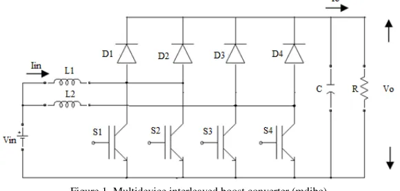
This Converter consists of n -phase interleaved with m switches connected in parallel per phase. The easy way to reduce the size of the inductor and capacitor is by increasing the frequency of the inductor current ripple and the output voltage ripple. With the proposed control, the switching pattern is shifted by 360 / (n × m), where m
is the number of parallel power switches per channel, and n is the number of channels or phases. The input current ripple is (n × m) times of the switching frequency. Similarly, the output voltage ripple is (n × m) times of the switching frequency. As a result, the size of the passive components will be reduced by m times compared with the n-phase interleaved boost converters. In this proposed Converter structure, m is selected to be 2, while n is selected to be 2.This Converter consists of two-phase interleaved with two switches and two diodes connected in parallel per phase.
Figure 1. Multidevice interleaved boost converter (mdibc)
2.3. Sequence of the Driving Gate Signals For Switches-
This control strategy will provide a doubled ripple frequency in inductor current at the same switching frequency. The sequence of the driving signals is very important to providing a doubled ripple frequency in inductor current at the same switching frequency and to achieve the interleaved control between inductors. As a result, the size of the passive components will be reduced by m times compared with the n-phase interleaved boost converters.
Volume 3 Issue 1 – March 2015 33 ISSN : 2319-6319 (a) (b)
Figure 2. (a) Gate signal, d= ts/4 (b) gate signal, d > ts/4
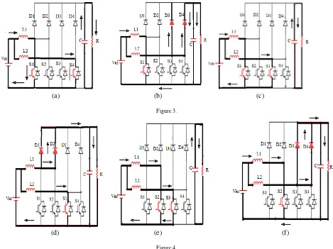
2.4. Modes of Operation-
It is assumed that the proposed Converter operates in the continuous conduction mode (CCM). The load current is assumed to be ripple free. All switches have identical duty ratios which means d1 = d2 = d3 = d4=d
(a) (b) (c)
Figure 3.
(d) (e) (f)
(g) (h)
Figure 3. EQUIVALENT CIRCUITS OF THE PROPOSED CONVERTER FOR D > 0.2 (a) Mode 1: 0 ≤ t ≤ d4 Ts (b) Mode 2: d4 Ts ≤ t ≤Ts /4 (c) Mode 3: Ts /4 ≤ t ≤ d1 Ts
(d) Mode 4: d1 Ts ≤ t ≤ Ts /2 (e) Mode 5: Tse /2 ≤ t ≤ d3 Ts (f) Mode 6: d3 Ts ≤ t ≤ 3 Ts /4 (g) Mode 7: 3 Ts /4 ≤ t ≤ d2Ts (h) Mode 8: d2 Ts ≤ t ≤ Ts
III. CONVERTER DESIGN CALCULATION 1. Average Output Voltage
Vo = Vin / (1-m*d) 2. Average input Current
Iin = Io / (1-m*d) 3. The peak-to-peak ripple Current
∆I = 2% of Iin 4. The peak-to-peak ripple Voltage
∆V = 2% of Vo
5. Input current ripple = (n × m) times of the switching frequency. 6. Output voltage ripple = (n × m) times of the switching frequency. 7. Efficiency(η) = Pout/(Pout + Plosses)
8. Plosses = PT + PD + PC 9. The output power is,
Pout = Vo Ioav 10. The losses of the switch ,
PT = {Isrms2rce + VceIsav +
Isrms = the rms current of the IGBT, Isav = the mean current of the IGBT
current ripple 11. The diode losses,
PD = I2Drmsrf + VFoIDav (IDav) Fs] ID rms = rms current of the diode
ID av = mean current of the diode 12. The losses of the passive components is,
Pc = I2LrmsRL + I2crmsRc
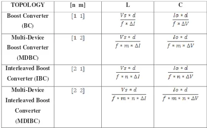
Volume 3 Issue 1 – March 2015 35 ISSN : 2319-6319 Table – 1 Comparison of BC,MDBC,IBC & MDIBC
TOPOLOGY
[n m]
L
C
Boost Converter
(BC)
Multi-Device
Boost Converter
(MDBC)
Interleaved Boost
Converter (IBC)
Multi-Device
Interleaved Boost
Converter
(MDIBC)
For an input voltage of 200 V, Switching frequency= 25KHz , d=0.25 system has the following output values 1. Output Voltage = 200/(1-(2*0.25)) = 400V
2. Output Power, Po = Vo2/R = 4002/10 = 1.6KW 3. Output Current, Io = Po/Vo = (1.6*103)/400 = 40A 4. Input Current, Iin = 40/(1-(2*0.25)) = 80A
5. The peak-to-peak ripple Current, ∆I = 0 .02*80 = 1.6A 6. The peak-to-peak ripple Voltage, ∆V = 0.02*400 = 8V 7. Inductor, L = (200*0.25)/(25000*2*2*1.6) = 2.5mH 8. Capacitor, C = (40*.25)/(25000*2*2*8) = 100µF
9. The inductor and capacitor values of different topologies are
Table - 2 L & C values of BC, MDBC, IBC & MDIBC
TOPOLOGY [n m] L (mH) C (µF)
BC 2.5 100
MDBC 1.25 50
IBC 1.25 50
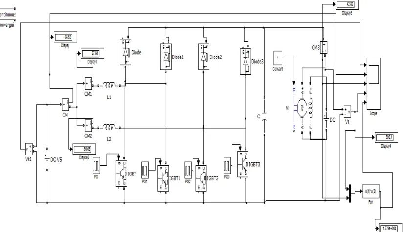
IV. SIMULATION MODEL 4.1. Simulation of Proposed Converter (MDIBC)-
A Converter circuit parameters are set up as following: 200V input voltage, 400V output voltage.
Figure 4. Simulation Circuit of Multidevice Interleaved Boost Converter Output Parameters:
Inductor = 0.625mH Capacitor = 25 µF Output Voltage = 392 V Input Current = 22 A Output Current = 42.82 A Output Power = 16.79 KW
V. RESULTS AND DISCUSSION The Result of different topologies are
Volume 3 Issue 1 – March 2015 37 ISSN : 2319-6319 VI.CONCLUSION
In this project, a novel MDIBC has been proposed. The advantages of the proposed Converter can be summarized as:
1) Size and weight of passive components (inductor and capacitor) are Reduced;
2) Reduced ripple current helps relieve stress on the output filter capacitors and increased effective switching frequency makes capacitors running Closer to their optimum;
3) Reliability and efficiency of the system are improved.
The simulation results have demonstrated that the inductor size and the capacitor size of the MDIBC are reduced by two times compared to the IBC. Also, the current and voltage ripples are reduced by two times compared with the IBC topology. The proposed Converter can improve efficiency and reduce the size of the components, leading to high reliability compared with other boost Converter (BC,MDBC,IBC) topologies.
REFERENCES
[1] “Analysis and Simulation of Interleaved Boost Converter for Automotive Applications” Farag. S.Alargt, Ahmed. S. Ashur, International Journal of Engineering and Innovative Technology (IJEIT) Volume 2, Issue 11, May2013
[2] O. Hegazy, J. Van Mierlo, and P. Lataire, “Analysis, control and implementation of a high-power interleaved boost Converter for fuel cell hybrid electric vehicle,” Int. Rev. Electr.Eng., vol. 6, no. 4, pp. 1739–1747, 2011.
[3] Omar Hegazy, Joeri Van Mierlo, and Philippe Lataire, “Analysis, Modeling, and Implementation of a Multidevice Interleaved DC/DC Converter for Fuel Cell Hybrid Electric Vehicles,” IEEE Trans. Ind. Electron., vol. 27, pp.4445–4457, Nov. 2012
[4] “Design and Analysis of Interleaved Boost Converter For Renewable Energy Applications” S. Kamtip and K. Bhumkittipich, 9th Eco-Energy and Materials Science and Engineering Symposium, Chiang Rai, Thailand 25-28 May. 2011
[5] Katsuhiko Ogata, “Modern Control Engineering”