Design And Simulation Of 10-Bit Pipeline
Adc Using Switch Capacitor Circuit And
Opamp Sharing In 0.25 µm CMOS
Technology at 2.5 V
Deepak Patidar#1, Mr. Piyush Moghe*2, Vijay Sharma#3
#
ME student1, Assistant Professor2,3, ECE Department)
SVCE, Indore (M.P)
Abstract—A 10-bit pipeline Analog-to-digital Converter
(ADC) is designed using switched capacitor circuit. ADC is designed in 9 stages, 1.5 bit/stage pipeline is used in eight stages and ninth stage uses two bit flash ADC. The ADC uses Opamp sharing techniques which are shared between amplifying and MDAC stage. Load capacitance has been removed which reduced the number of capacitors used and power consumption. The ADC is designed on 0.25 µm CMOS technology at 2.5 V supply voltage. S/H is used in first stages that consume most of the power consumed by the ADC, after first stage S/H circuit is removed, and also the scaling is done to reduce the power consumption. Cascodeopamp is designed with gain of 72.52 dB, phase margin of 66º and unity gain bandwidth of 162.61MHz. The ADC is designed at
sampling rate of 5 MS/s and consumes
158.1208mWpower.
Keywords —ADC, MDAC, sample and hold, pipeline ADC, DAC
.
I. INTRODUCTION (SIZE 10&BOLD) Advantages of digital systems over analog systems made it popular in system designing, but the natural signals are analog in nature that is why it becomes important to have a system which can convert the analog signal into the digital signals. Analog to digital converts are such circuits which can connect the analog domain into the digital domain. There are various types of ADCs which are used and every ADC has its own advantages and disadvantages. Pipeline ADC can resolve medium to high resolution at higher speed. Which make it popular for modern digital systems where high resolution with higher speed is required.
Pipeline ADC uses several stages to convert analog signal to digital signal every stage has flash ADC of 1 to 3 bit and converts portion of input signal to output. The first stage produces most significant bit (MSB) while the last stage produces least significant bit (LSB).
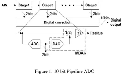
Figure 1: 10-bit Pipeline ADC
II. PIPELINE ADC ARCHITECTURE
The pipeline ADC is consist of cascade of low resolution stages that generates parallel ADC output and residue signal for next stage. Residue is un-quantized output which is the output of subtraction of input signal and the digital to analog (DAC) signal. The architecture of the 10-bit pipeline ADC is shown in figure 1. In pipeline ADC each stage consist of low resolution flash ADC, DAC and subtractor, DAC consist of multiplying digital to analog converter (MDAC) that converters digital signal to analog signal followed by the amplifier. The residue generated from first stage goes to next stage, for 10-bit ADC eight stages are of 1.5 bit/stage and the last stage uses two bit flash ADC.
To synchronize the output of the stages delay elements is used which reduces with the stage, last stage does not require MDAC and delay element. Each stage has two output lines which is later given to the error correction block that generates the 10-bit output lines. The block diagram of MDAC is shown in the figure 2.
III.1.5 BIT/STAGE PIPELINE
Figure 2 : Pipeline ADC Block diagram for 1.5 bits/stage
If comparator threshold offsets forces the residue signal to fall outside normal range, the residue signal will be accurately passed into the next stage provided the offset is within
V
ref/ 4
. Figure 3demonstrates this by showing the transfer function of a 1.5-bit MDAC when there are threshold offsets in the sub-ADC. The fourth level is removed because the MDAC only needs to indicate whether the residue output is above or below
V
ref/ 2
andtherefore, there is only an overlap of half bit. The accuracy of the 1.5-bit sub-ADC reduces from N bit to 2 bits using DEC. Generally, by using DEC, the accuracy of the sub-ADC can be increase if fewer bits are resolved in each stage.
Figure 3: Transfer function of 1.5 bits/stage MDAC [12]
The pipeline ADC applies DEC and consists of a front-end S/H, 8 pipeline stages, and a 2-bit flash ADC in last stage. Each pipeline stage resolves 1.5 Bits/stage, which is represented by a 2 output lines of single bit. In the end, a total of 18-bits are generated from a single input sample. To apply DEC, the bits from each adjacent pipeline stage Overlap by half a bit and form the expected 4-bit output.
Figure 4: Transfer function of a 1.5 bit/stage MDAC with comparator with offset
IV.CASCODE OPAMP
Cascade opamp is used for the pipeline ADC design the opamp is designed in two stages first stage is the preamplifing stage that provides most of the gains and has higher input impedance.
A. Gain
The settling accuracy refers to how close the residue output settles to its intended value and therefore, it can limit the accuracy of the ADC. Assuming the opamp has sufficient time to settle to its final value, the opamp’s open-loop gain, A, sets the settling accuracy. This is because a higher open-loop gain results in a more accurate stage gain and in turn, the residue output follows a more accurate transfer function. To ensure the residue settles to withLSB, the loop gain of the
closed-loop, A
, must be: 2N
A
Where
is thefeedback factor of the closed-loop circuit and 1
1 2N
LSB . The loop gain, as the name suggests, is the
gain around the opamp closed-loop circuit. Considering there are other sources of error (e.g. thermal noise), a reasonable choice is
0.25
LSB
. For instance, the front-end sample and hold and first pipeline stage in a 4-bit pipeline ADC requires a loop gain of:10 2
4096
0.25 or72dB
B. Bandwidth
Figure 5 Schematic of Opamp [27]
The bandwidth of the opamp closed-loop circuit,
3dB
f
, so that the residue settles to within 0.5 LSB in half a sampling period.3
(
1).ln 2.
SdB
N
f
f
The frequency response opamp is shown in the figure 7
.
Figure 6: Bias Circuit for Opamp
1 10 100 1k 10k 100k 1M 10M 100M 1G
Frequency (Hz)
-100 -50 0 50 100 150 200
Vo
lt
a
g
e
Ph
a
se
(d
e
g
)
vp(Out) Opamp Phase Plot
1 10 100 1k 10k 100k 1M 10M 100M 1G
Frequency (Hz)
0 10 20 30 40 50 60 70 80
Vo
lt
a
g
e
M
a
g
n
it
u
d
e
(
d
B)
vdb(Out) Gain: 78.59 dB
UGB: 857.59 MHz Opamp Gain Plot (dB)
Figure 7: Frequency response of Opamp
V. COMPARATOR DESIGN
The comparator is unclocked of three stages, pre-amplification, decision circuit and output buffer. Pre-amplification stage consist of differential input stage with active PMOS load. M1 and M2 NMOS transistor act as input it also provides the high input impedance, it also improves the sensitivity.
Decision circuit uses positive feedback that increases the gain, cascading of pre-amplification and decision circuit increases the gain with large amount. To make the output compatible with the digital circuit output stage is used which uses inverter it also provides small gain. The transfer characteristics of comparator is shown in the figure 9
.
Figure 8: Schematic of Comparator
0.0 0.5 1.0 1.5 2.0 2.5
VVin (V)
-2.0 -1.5 -1.0 -0.5 0.0 0.5 1.0 1.5 2.0 2.5
V
o
lt
a
g
e
(
V
)
v(Out) first_bit_ADC
Figure 9: DC transfer characteristics of Comparator
VI. NON-OVERLAPPING CLOCK
GENERATOR
Non-overlapping clock is required for the MDAC switch capacitor circuits and sample and hold circuit. The schematics of non-overlapping is shown in the figure 10. The response of the non-overlapping clock is shown in the figure 11.
VII. SAMPLE AND HOLD CIRCUIT
Figure10: Schematic of Non Overlapping clock
0.2025 0.2030 0.2035 0.2040
Time (us)
0.0 0.5 1.0 1.5 2.0 2.5
V
o
lt
a
g
e
(
V
)
v(Phi_2_p)
v(Phi_1) v(Phi_2) v(Phi_1_p)
Delay: 806.08 ps Non_Overlap_clock
Figure 11: Transient response of non-overlapping clock
1
clock connects the output of the opmap to ground by triggering the M1 transistor, which discharge the initial charge stored in the opamp at the same clock pulse input is connected to the top plate of the capacitor C1, the input is stored in the capacitor in the form of charge. At this time signal is sampled and stored in the capacitor.Figure 12: Switched capacitor sample and hold circuit
At
2capacitor top plate is connected to the output of opamp and charge stored at the capacitor is transferred to the output. The transient response of sample and hold circuit is shown in the figure 13.VIII. MULTIPLYING DIGITAL TO
ANALOG CONVERTER (MDAC)
Figure 14.shows the schematic of Multiplying Digital to Analog (MDAC) using a switched capacitor approach.[10].
10 11 12 13 14 15 16 17 18 19 20
Time (us)
-0.1 -0.0 0.1 0.2 0.3 0.4 0.5 0.6 0.7 0.8 0.9 1.0
V
o
lta
g
e
(
V
)
v(In)
v(Out) Sample_Hold
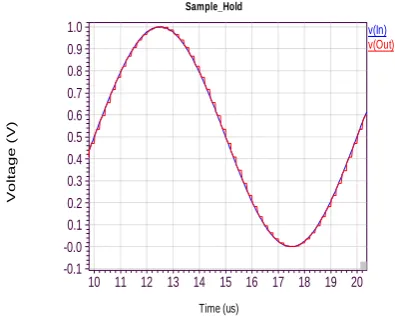
Figure 13: Transient response of sample and Hold circuit
Since 1.5 bits/stage architecture has one of three digital outputs, thus the DAC has three operating modes.
ADC output=01: No over range error (stage input is
between
4
ref
V
and4
ref
V
).During
1:Q
C1
C V Q
1 in, C2
C V
2 inDuring
2 : C1 is discharged, thus by chargeconservation:
C V
1 in
C V
2 in
C V
2 out(noting negative feedback forces node Vp to a virtual
ground) Thus
1 2
1 2,
2
:
2
out in out in
C
C
V
V
ifC
C then V
V
C
Figure 14: Schematic of MDAC
ADC output=10: Over range error-Input
exceeds
4
ref
V
, thus subtract2
ref
V
from input
During
1:Q
C1
C V Q
1 in,
C2
C V
2 inDuring
2: C1 is charged to Vref, thus by charge conservation1 in 2 in 1 ref 2 out
1 2 1
1 2
2 2
, , : 2 2( / 2)
out in ref out in ref in ref
C C C
V V V if C C then V V V V V
C C
ADC output=00: Under range error-Input
below
4
ref
V
, thus add2
ref
V
to input
During
1:Q
C1
C V Q
1 in,
C2
C V
2 inDuring
2: C1 is charged to –Vref. Thus by chargeconservation
C V
1 in
C V
2 in
C
1(
V
ref)
C V
2 outThus the switched capacitor circuit can be used to implement the sample-and-hold, gain stage, DAC, and subtraction blocks of ADC. To reduce the signal dependent charge injection bottom plate sampling technique is where the use of an advanced clock
1p,makes charge injection signal independent [10]. The total input sampling capacitance in
1
isC
iT MDAC,
C
1.5 10 15 20
Time (us) -0.7 -0.6 -0.5 -0.4 -0.3 -0.2 -0.1 -0.0 0.1 0.2 0.3 0.4 0.5 V o lta g e ( V ) v(In) Sample _Hold
5 10 15 20
Time (us) -0.7 -0.6 -0.5 -0.4 -0.3 -0.2 -0.1 -0.0 0.1 0.2 0.3 0.4 0.5 V o lta g e ( V ) v(Out) Sample _Hold
Figure 15: Transient response of MDAC for sinusoidal signal
In
2 , the twoC
1/ 2
capacitors apply a load of1
/ 4
C
on the MDAC opamp. Taking into consideration the loading effects of the next stage and of the parasitic ccapacitanceC
n2 , the total output load on the MDAC opamp is:, 1
/ 4
, , 2L flipMDAC iT subADC iT nextstageMDAC n
C
C
C
C
C
Transient response of MDAC is shown in the figure 15
.
IX.10-BIT PIPELINE ADC
A. Sub analog to digital converter
Sub ADC is a 1.5 bit Flash ADC in which two comparators are used to compare the input signal
with two reference voltages
4
refV
and4
refV
Figure 16 Schematic of sub ADC
Respectively as shown in Figure 16. The reference voltage selected in this ADC is 1V which means the
V
ref =0.25 V and
V
ref =-0.25 V [6]. Itgenerates the thermometer code at the output of the comparators that need to convert into the binary code. This can be converted by adding thermometer to binary encoder circuit. Transient response of sub ADC is shown in the figure 17.
B. First stage pipeline ADC
First stage pipeline ADC is shown in figure 18 first stage have sample and hold which samples the input signal, sampled signal is given to sub ADC which converted it to digital signal. MDAC converts this digital signal to analog signal the switches of MDAC
0 1 2 3 4 5 6 7 8 9 10
T i me (us)
-1.0 -0.5 0.0 0.5 1.0 V o lt a g e ( V ) v(In ) first_b it_ADC
0 1 2 3 4 5 6 7 8 9 10
T i me (us)
-2.5 -2.0 -1.5 -1.0 -0.5 0.0 0.5 1.0 1.5 2.0 2.5 V o lt a g e ( V ) v(B1) first_b it_ADC
0 1 2 3 4 5 6 7 8 9 10
T i me (us)
0.0 0.5 1.0 1.5 2.0 2.5 V o lt a g e ( V ) v(B0) first_b it_ADC
Figure 17: Transient response of sub ADC
Figure 18: Block diagram of first stage pipeline ADC [18]
0 1 2 3 4 5 6 7 8 9 10
Time (us)
0.0 0.5 1.0 1.5 2.0 2.5
V
olt
age
(V)
v(Z)
fir st_ bit_ ADC
0 1 2 3 4 5 6 7 8 9 10
Time (us)
0.0 0.5 1.0 1.5 2.0 2.5
V
olt
age
(V)
v(Y) fir st_ bit_ ADC
0 1 2 3 4 5 6 7 8 9 10
Time (us)
0.0 0.5 1.0 1.5 2.0 2.5
V
olt
age
(V)
v(X) fir st_ bit_ ADC
0 1 2 3 4 5 6 7 8 9 10
Time (us)
-1.0 -0.5 0.0 0.5 1.0
V
olt
age
(V)
v(In) fir st_ bit_ ADC
Figure 19: Transient response of first stage pipeline ADC
The transient response of first stage pipeline ADC is shown in the figure 19.
Figure 20: 10-bit pipeline ADC test setup
C. 10-bit pipeline ADC
The complete schematic of 4-bit pipeline ADC is shown in figure 20, First and second stage are identical and sampled capacitor C2 =C1= 1 µF is used. After second stage scaling is done to reduce the power consumption and uses C1=C2=0.5 µF and 0.25 µF for third, fourth stage respectively
0.0 0.1 0.2 0.3 0.4 0.5 0.6 0.7 0.8 0.9 1.0
Time (us)
0.0 0.5 1.0 1.5 2.0 2.5
V
ol
tag
e
(V
)
v(B8) v(B7)
v(B6)
v(B5) v(B4)
v(B3)
v(B2)
v(B1) v(B0) v(B10)
v(B9) ADC_Test
Figure 21: Transient response of 10-bit pipeline ADC
Transient response of 10-bit pipeline ADC is shown in figure 21.
X. PERFORMANCE SUMMARY
Technology
0.25 µm CMOS process
Resolution
10 bit
Supply Voltage
2.5 V
Conversion rate 5 MS/s
Power
158.1208
XI.CONCLUSION
The goal of this dissertation was to design a 2.5 V, 1.5 bit/stage 4bit ADC by using switched capacitor technique. The ADC is designed in 0.25 µm CMOS process at 2.5 V supply voltage. It also shows the comparison between the power consumption of stages with the S/H and without S/H which gives 28.33 mW in first stage (with S/H) and 19.59 mW third stage (without S/H).Further the ADC is tested at input frequency of 1 MHz and sampling rate of 5 MS/s, at which ADC consumes 158.12mW power.
REFERENCES
[1] J. Yuan, S.W. Fung, “A 12-bit 20 MS/s 56.3 mW Pipelined
ADC With Interpolation-Based Nonlinear Calibration”, IEEE
Transactions on circuits and systems, Regular paper, Vol. 59, No. 3, March 2012.
[2] Y. Lin, K. Doris, “An 11b Pipeline ADC With
Parallel-Sampling Technique for Converting Multi-Carrier Signals”, IEEE
Transactions on circuits and systems, Regular paper, Vol. 59, No. 5, May 2012.
[3] N. Sun, “Exploiting Process Variation and Noise in Comparators to Calibrate Interstage Gain Nonlinearity in Pipelined ADCs”, IEEE Transactions on circuits and systems,
Regular paper, Vol. 59, No. 4, April 2012.
[4] T. Miki, T. Morie, “An 11-b 300-MS/s Double-Sampling Pipelined ADC With On-Chip Digital Calibration for Memory Effects”, IEEE Journal of solid state circuits, Vol. 47, No. 11, November 2012.
[6] S. Lee, A.P. Chandrakasan, “A 12 b 5-to-50 MS/s 0.5-to-1 V
Voltage Scalable Zero-Crossing Based Pipeline ADC”, IEEE
Journal of solid state circuits, Vol. 47, No. 7, July 2012. [7] C.y. Chen, J. Wu, “A 12-Bit 3 GS/s Pipeline ADC With 0.4 mm2 and 500 mW in 40 nm Digital CMOS”, IEEE Journal of
solid state circuits, Vol. 47, No. 4, April 2012.
[8] T. Sundstrom, C. Svensson, “A 2.4 GS/s, Single-Channel, 31.3 dB SNDR at Nyquist, Pipeline ADC in 65 nm CMOS”,
IEEE Journal of solid state circuits, Vol. 46, No. 7, July 2011. [9] J. Yuan, S.W. Fung, “An Interpolation-Based Calibration
Architecture for Pipeline ADC With Nonlinear Error”, IEEE
Transactions on instrumentation and measurement, Vol.61, No.1, January 2012.
[10] C.J. Tseng, H.W. Chen, “A 10-bit 320-MS/s Stage-Gain-Error Self-Calibration Pipeline ADC”, IEEE Journal of solid state circuits, Vol. 47, No. 6, June 2012.
[11] C.S Shin, G.C. Ahn, “A 10-bit 100-MS/s Dual-Channel Pipeline ADC Using Dynamic Memory Effect Cancellation technique”, IEEE Transactions on circuit and system, Express Briefs, Vol. 58, No. 5, May 2011.
[12] K. Chandrashekar, M. Corsi, “A 20-MS/s to 40-MS/s Reconfigurable Pipeline ADC Implemented With Parallel OTA Scaling”, IEEE Transactions on circuits and systems, Express briefs, Vol. 57, No. 8, August 2010.
[13] S. Devarajan, L. Singer, “A 16-bit, 125 MS/s, 385 mW, 78.7
dB SNR CMOS Pipeline ADC”, IEEE Journal of solid state
circuits, Vol. 44, No. 12, December 2009.
[14] A. Verma, B. Razavi, “A 10-Bit 500-MS/s 55-mW CMOS ADC”, IEEE Journal of solid state circuits, Vol. 44, No. 11, November 2009.
[15] N. Sasidhar, Y.J. Kook, “A Low Power Pipeline ADC Using Capacitor and Opamp Sharing Technique With a Scheme to
Cancel the Effect of Signal Dependent Kickback”, IEEE Journal
of solid state circuits, Vol. 44, No. 9, September 2009.
[16] B.G. Lee, R.M Tsang, “A 10-bit 50 MS/s Pipelined ADC
With Capacitor-Sharing and Variable- .
g
m Opamp”, IEEEJournal of solid state circuits, Vol. 44, No. 3, March 2009. [17] B.G.Lee , B.M.Min, “A 14-bit 100 MS/s Pipeline ADC with a Merged SHA and First MDAC”, IEEE Journal of solid state circuits, Vol.24, No. 12, December 2008.
[18] K. Honda, M. Furuta, “A Low-Power Low-Voltage 10-bit 100-MSample/s Pipeline A/D Converter Using Capacitance Coupling Techniques”, .IEEE Journal of solid state circuits, Vol.24, No. 4, December 2007.
[19] S.T. Ryu, B.S. Song, “A 10-bit 50-MS/s Pipeline ADC
WithOpamp Current Reuse”, IEEE Journal of solid state circuits,
Vol.42, No. 3, March 2007.
[20] D. Kurose, T. Ito, “55-mW 200-MSPS 10-bit Pipeline ADCs for Wireless Receivers”, IEEE Journal of solid state circuits, Vol.41, No. 7, July 2006.
[21] I. Ahmed, “Pipeline ADC Design and Enhancement Techniques”, Springer publication-2010, Ch-3, pp-19-36. [22] M.J.M. Pelgrom, “Analog-to-Digital Conversion”, Springer publication- 2010, Ch 7,8, pp-203-318.
[23] M. Gustavsson, J.J Wikner, and N.N Tan, “CMOS Data
Converters for Communication”, Kluwer Academic
Publishers-2002, Ch-1,5, pp-1-25 and 125-137.
[24] R.V.D. Plassche, “CMOS Integrated Analog-to-Digital and
Digital-to-Analog Converters”, Kluwer Academic
Publishers-Second Edition, Ch-13, pp-523-549.
[25] J.R. Amaya, M.D. Restituto, A.R. Vazquez, “Device-Level Modeling and Synthesis of High-Performance Pipeline ADCs”,
Springer-2011, Ch-1,2, pp-1-25 and 29-34.
[26] J. Baker, “CMOS Circuit Design, Layout, and Simulation”,
Wiley Indian Edition second Edition,Ch-27, pp-909-928. [27] M.J. Demler , “HighispeedAnalog-to-Digital Conversion”,
Academic Press, Inc.-1991, Ch-1, pp-1-19,
[28] B. Razavi, “Principal of Data Conversion System Design”,
IEEE Press Circuit and System society,Ch-6, pp-96-147. [29] G. Zhang, “A Low-Power Pipeline ADC with Front-End Capacitor Sharing”, Master of Applied Science thesis University of Toronto, Ch-3, pp-17-26.
[30]http://www.maximintegrated.com/app-notes/index.mvp/id/283.
[31] P.E. Allen, D.R. Holberg, “CMOS Analog Circuit Design”,
International student edition oxford university press-2010, Ch-8,9, pp-439-483 and 492-561.
[32] B. Razavi, “Design of Analog CMOS Integrated Circuits”,
![Figure 3: Transfer function of 1.5 bits/stage MDAC [12]](https://thumb-us.123doks.com/thumbv2/123dok_us/8590644.1721080/2.595.314.514.70.243/figure-transfer-function-bits-stage-mdac.webp)
![Figure 5 Schematic of Opamp [27]](https://thumb-us.123doks.com/thumbv2/123dok_us/8590644.1721080/3.595.83.285.77.259/figure-schematic-of-opamp.webp)

![Figure 18: Block diagram of first stage pipeline ADC [18]](https://thumb-us.123doks.com/thumbv2/123dok_us/8590644.1721080/6.595.318.512.77.207/figure-block-diagram-stage-pipeline-adc.webp)
