A Efficient Technique For Low-Power High
Speed Adder Circuit Design in DSM
Technology
Anuj Dev
#1, Sandip Nimade
#2,
# PG Student [VLSI], Dept. of ECE
,
Technocrats Institute of Technology Bhopal, IndiaRGPV Bhopal, M.P. India
Abstract:- The necessity for low-power design is also important in high performance digital systems, such as microprocessors and digital signal processors because of high integration density and the high clock frequency. In this paper we presented a new 13T full adder design based on hybrid – CMOS logic design style. The new design is compared with some existing designs for power consumption, delay, PDP at various frequencies such as 10 MHz, 200 MHz and 1 GHz. the simulations are carried out on Cadence Virtuoso at 65nm CMOS technology and the simulation results are analyzed to verify the superiority of the proposed design over the existing designs. Maximum saving of power delay product is at low frequency by proposed circuit is 90.8% with respect to C-CMOS and significant improvement is observed at other frequencies also for proper validation and verification of the results W/L ratio of all the circuit is kept constant.
Keywords - Low power, GDI, SERF, Hybrid adder
I.
INTRODUCTION
Efficiency of implementation of arithmetic circuits in the execution of dedicated algorithms such as digital filtering, correlation and convolution largely affects the performance of application specific integrated circuits and digital signal processors. The GDI cell is similar to a CMOS inverter structure. In a CMOS inverter, the supply voltage (Vdd) and the
ground voltage (Vss) are connected to the source of
the pMOS and nMOS respectively whereas in a GDI cell it is not necessary to connect supply and ground voltage with MOS diffusions. There are few other differences between the two cells. The three inputs in GDI cell are G, P and N. The „G‟ is the common inputs to the gate of nMOS and pMOS, „N‟ is the input to the source/drain of nMOS and „P‟ is the input to the source/drain of pMOS. The Bulks of both nMOS and pMOS are connected to „N‟ or „P‟inputs so that it can be randomly biased unlike in CMOS inverter. Moreover, the most important difference between CMOS and GDI is that in GDI N,
P and G terminals could be given a supply „Vdd‟ or
can be grounded or can be supplied with input signal depending upon the circuit to be designed and hence effectively minimizing the number of transistors used in case of most logic circuits. Basic gates such as AND, OR, and MUX can be design using only two transistors. As the allotment of supply and ground to pMOS and nMOS is not fixed in case of GDI, therefore, problem of low voltage swing arises in GDI which is a drawback and hence finds difficulty in case of implementation of complex digital circuits.
consist of the simulation results and conclusion respectively.
II. Literature Review of Full Adder
Circuit Designs
As the Designing of digital circuit design various technique is introduce for power optimization methods at various level of digital circuit design process from system level to physical level. Different sources responsible for power dissipation in CMOS circuits are also reviewed. Here a various adder circuit design is study by different authors for low power and high speed.
A.Bazzazi and B. Eskafi, 2010 [13], proposed a 24 transistor one bit full adder using GDI based XOR – XNOR functions. The post layout simulation of adder with HSPICE tool at 0.18 µm CMOS technology shows great improvement in terms of power-delay product. The power dissipation is also very less as compared to other logic styles.
T. Kalavathidevi and C. Venkatesh,2011 [14],
implemented a Viterbi decoder using GDI cell at 0.25μm technology with 3.5V Vddand a frequency of
35MHz. The outputs of the convolutional encoder designed for the constraint lengths are fed to the designed Viterbi decoder. The comparison results showed 28% reduction in power consumption and 67% reduction in area by using GDI circuit than the CMOS circuit.
Prathyusha Konduri and MageshKannan.P, 2011 [15] shows the implementation of RAM in GDI technique and its simulation is done in 0.18μm TSMC technology with the supply voltage of 1.8V. Their result shows 16% reduction in power and 49% reduction in delay as compared with traditional CMOS technique.
R.Uma and P. Dhavachelvan, 2012 [16],
introduced Modified Gate Diffusion Input (MGDI) Technique. They presented new design structure of basic digital gates using two transistors for AND, OR, XOR, NAND, NOR and XNOR gates. Design is compared with basic GDI technique.
Vahid Foroutanet. al.,2014 [17], presented two new symmetric designs for low- power, high speed
Diode) logic-level restorer is used in adders for full-voltage swing. The circuits are optimized for energy efficiency at 0.13 µm and 90 nm partially depleted (PD) SOI CMOS process technology. Simulations performed on HSPICE and the comparison with standard full adder cells shows excessive improvement in terms of Power, Area, Delay and Power-Delay-Product (PDP).
The conventional CMOS full adder comprises of a regular CMOS structure of 28 transistors with usual pull-up and pull-down networks as shown in Figure.1 [7]. The complementary design of CMOS full adder accounts for full output voltage swing and its robustness against voltage scaling and transistor sizing is one of its main advantages. The main drawback of C-CMOS adder is its large input capacitance due to the utilization of large number of PMOS transistors in its design. The large number of PMOS transistors also increases the chip area required for the circuit.
A A A A
A A
A A
B
B
B
B
B B
B Cin
Cin
Cin Cin
Cin Cin
Sum
Carry
B
Figure.1: Circuit structure for complementary CMOS (C-CMOS)
G
P
N
OUT = G’P + GN
(a)
B
A B
M1
M2
M3
M4
Ci M5
M6
M7
M8
M9
M10
VDD
VDD
(b)
Figure. 2: (a). Basic GDI cell (b). 10 Transistor design of a GDI based adder
The floating adder circuit comprises of 8 transistors as shown in the Figure. 3. As can be seen from the structure of the floating adder two of the internal nodes (X and Y) are kept floating i.e. not directly connected to any of the input terminals hence it is being named as “floating adder”. The power in the circuit increases at a lower rate with increase of operating frequency of the circuit as compared to other high power designs. The principle demerit of this circuit is the degraded output voltage level i.e the weak „1‟ and „0‟ at the carry and sum output respectively which leads to the poor driving capability of the adder circuit but this can be sorted out using buffers at the output stages[10].
A B
B B
A
A Ci
Ci Ci
X
Y
MNFD1
MNFD2
MNFD3
MNFD4 MPFD1
MPFD2
MPFD3
MPFD4
Figure.3: Structure of a floating adder The hybrid logic design style combines the advantages of multiple logic styles to carry out a design with optimized desired performance characteristics. A hybrid adder utilizing the advantages of pass transistor technique and transmission gate technique is shown in Figure.4 [11, 12] this adder comprises of 16 transistors and provides low power high speed performance with considerable logic swing and satisfactory performance stability with frequency variations. The number of transistors used in the adder can be further reduced in hybrid logic design style to reduce the chip area and power consumption in the adder[13,14].
Cin
B
A Vdd
Sum
Carry Vdd
III. Proposed Adder Circuit
The hybrid logic design style involves the division of larger circuit into smaller sub-circuits and each sub-circuit is optimized using various logic design style. The hybrid design methodology for a full adder circuit is shown in Figure.5. As shown in the figure the full adder circuit is divided into three modules and these modules are designed using various different design styles to exploit the advantages of the different design styles and extract the desired performance. Module 1 produces XNOR and XOR functions of the inputs A and B [15,16]. the module1 can be either XNOR based or XOR based depending on the primary output generated within the module the primary output is utilized to get the other output using an inverter. Module 2 and Module 3 comprises of the circuitry to produce the desired sum and carry outputs of the full adder by utilizing the intermediate outputs generated by Module 1 circuit.
Module 1
A
B
Module 2
Module 3
Cin
Sum
Carry
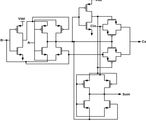
Figure.5: Hybrid design methodology In this paper a 13 transistor design of a single bit full adder based on Hybrid GDI logic design style is been proposed as shown in Figure.6. As the design suggests the proposed adder circuit exploits the advantages of GDI technique, pass transistor technique and transmission gate technique to carryout excellent low power and high speed characteristics.
3.1 Module 1
The module 1 of the proposed circuit is XNOR based producing XNOR function as its primary output and then using an inverter to get the XOR function from the primary XNOR output. The XNOR and XOR outputs from module 1 are utilized by the Transmission gates in module2 and module 3 to produce the sum and carry outputs of the full adder.
Vdd B
Cin
SUM
Carry B
A
MN1
MN2 MP1
MP2
MN3
MN4 MN5
MP3 MP4
MP5 MP6
MN6 MN7
Figure.6: Proposed XNOR based full adder circuit
Figure.7: Transient response of Proposed Circuit The output of the 3T GDI XNOR gate is defined by Table. 1 below
[1]. Table 1 Truth Table of the 3T GDI XNOR gate
Inputs output
A B Logic Voltage level 0 0 1 Vdd
0 1 0 Gnd 1 0 0 Vtn
1 1 1 Vin-Vtn to Vdd
3.2 Module 2
obvious reasons of practical applicability and the fan out of the circuit as the adder is never used as a single unit it is always used in multiples so as to perform arithmetic operation in a processor which is never a single bit case. The module 2 must also consume lower power although we can make a trade off with power and area to maintain the voltage swing at the output. The design of the module 2 is in accordance with the equation 3.1 and As the figure suggest module 2 is designed with four transistors two form a transmission gate(MN6 and MP7) and two form a pass transistor structure with complementary inputs.
…3.1
The complementary structure of the design contributes to the full output swing so as to provide good driving capability.
3.3 Module 3
The module 3 of the proposed design is the carry generating circuit. The carry generating circuit should produce an output with full voltage swing for all the obvious reasons of practical applicability and the fan out of the circuit, because the adder is never used as a single unit it is always used in multiples so as to perform arithmetic operation in a processor which is never a single bit case. One more aspect that has to be kept in mind while designing the carry generating circuit is that the path of the input carry to output carry must be as small as possible as it is directly related to the delay of the circuit.
The design of the module 3 is in accordance with the equation 3.2. As the figure suggest module 2 is designed with four transistors forming two transmission gates.
…3.3.2
The operation of the proposed circuit is simple that the module 1 constituted by 5 transistors namely (MN1, MN2, MN3, MP1 and MP2) produces intermediate XOR and XNOR outputs. The additional PMOS (MP1) applied in the module 1 ensures the proper logic and also tend to mitigate the effect of voltage degradation on its output. The XOR and XNOR output generated by the module 1 circuit are fed to the module 2 for generating the sum output of the full adder in accordance with the equation 3.1 and to module 3 for generating the carry output of the full adder in accordance with the equation 3.2.
IV. SIMULATION RESULTS
All the circuit is simulated by using Specter Cadence virtuoso tool at 65nm technology with 1V supply voltage. The circuits are being simulated at different operating frequencies namely 100 MHz, 200MHz and 1GHz to analyze the effect of change of operating frequency on reference as well as proposed circuits. The high speed operation is also analyzed by simulating at a frequency as high as 1GHz.
Table 4.1-4.3 show the results obtained during the simulation of the various adder circuits and proposed circuits. From the tabular comparison presented below it can easily be seen that the proposed circuit show improvements in both power consumption and propagation delay of the circuits and hence an improved power delay product (figure of merit in a digital circuit) is observed.
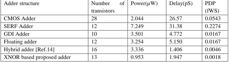
Table 4.1 Comparison of the proposed circuits with some previously known low power full adder circuits at 100 MHz operating frequency.
Adder structure Number of transistors
Table 4.2 Comparison of the proposed circuits with some previously known low power full adder circuits at 200 MHz operating frequency
Adder structure Number of transistors
Power(µ W)
Delay(pS) PDP(fWS )
CMOS 28 3.977 25.97 0.1032 SERF Adder 12 10.72 30.25 0.3242 GDI Adder 10 4.535 2.598 0.0117 Floating adder 12 5.990 4.782 0.0286 Hybrid adder [Ref.14] 16 5.605 1.487 0.0083 XNOR based proposed adder 13 1.26 2.066 0.0026
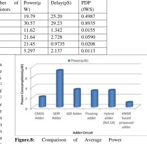
Table 4.3 Comparison of the proposed circuits with some previously known low power full adder circuits at 1 GHz operating frequency
Adder structure Number of transistors
Power(µ W)
Delay(pS) PDP (fWS) CMOS 28 19.79 25.20 0.4987 SERF Adder 12 30.57 29.23 0.8935 GDI Adder 10 11.62 1.342 0.0155 Floating adder 12 21.64 2.728 0.0590 Hybrid adder [Ref.14] 16 21.45 0.9735 0.0208 XNOR based proposed adder 13 5.297 2.137 0.0113 the proposed XNOR based full adder circuit saves a
maximum power of 86.8% in comparison to the SERF adder and a maximum improvement of 93.7% in propagation delay in comparison to the SERF adder moreover a maximum improvement of 99.2 % is observed in PDP in comparison to SERF adder at 100 MHz frequency. At 200 MHz frequency, the proposed XNOR based full adder circuit saves a maximum power of 88.2% in comparison to the SERF adder and a maximum improvement of 93.1% in propagation delay in comparison to the SERF adder moreover a maximum improvement of 99.1 % is observed in PDP in comparison to SERF adder. When the frequency is increased up to 1GHz even at this high operating frequency, the proposed XNOR based full adder circuit saves a maximum power of 82.67% in comparison to the SERF adder and a maximum improvement of 92.6% in propagation delay in comparison to the SERF adder moreover a maximum improvement of 98.7 % is observed in PDP in comparison to SERF adder. The results in Table 4.1-4.3 also reveal that, as the frequency increases power consumption in all the adder circuits increases. Although in the proposed circuits the rate of increase of power consumption with frequency is lower than that in case of previously known adders, i.e. in all the reference adders shown in observation
Figure.8: Comparison of Average Power Consumption of Adder Circuit
V. CONCLUSION
maximum of 99.2 %in comparison to SERF adder at 100 MHz frequency. Basic gates and important building blocks of digital systems such as full adder, carry propagate adder, magnitude comparator, arithmetic logic unit, binary multiplier and booth encoded multiplier are designed using Hybrid GDI gates.
References
[1] U. Ko, P. Balsara, and W. Lee, “Low-power design techniques for high-performance CMOS adders,” IEEE Trans. Very Large Scale Integr. (VLSI) Syst., vol. 3, no. 2, pp. 327–333, Jun. 1995.
[2] A. Shams, T. Darwish, and M. Bayoumi, “Performance analysis of low power 1-bit CMOS full adder cells,” IEEE Trans. Very Large Scale Integr. (VLSI) Syst., vol. 10, no. 1, pp. 20–29, Feb. 2002.
[3] M. Alioto and G. Palumbo, “Analysis and comparison on full adder block in submicron technology,” IEEE Trans. Very Large Scale (VLSI) Syst., vol. 10, no. 6, pp. 806–823, Dec. 2002.
[4] P. J. Song and G. De Micheli, “Circuit and architecture trade-offs for high-speed multiplication,” IEEE J. Solid-State Circuits, vol. 26, no. 9, pp. 1184–1198, Sep. 1991.
[5] A. P. Chandrakasan and R. W. Brodersen, Low Power Digital CMOS Design. Norwell, MA: Kluwer, 1995.
[6] Z. Wang, G. Jullien, and W. C. Miller, “A new design technique for column compression multipliers,” IEEE Trans. Comput., vol. 44, no. 8, pp. 962–970, Aug. 1995.
[7] R. Zimmermann and W. Fichtner, “Low-power logic styles: CMOS versus pass-transistor logic,” IEEE J. Solid-State Circuits, vol. 32, pp. 1079–90, July 1997.
[8] Vahid Foroutan, Mohammad Reza Taheri, Keivan Navi, Arash Azizi Mazreah “ Design of two Low-Power full adder cells using GDI structure and hybrid CMOS logic style”,Integration, the VLSI Journal, Vol.47,no.1, pp 48-61 January 2014.
[9] R. Uma and P. Dhavachelvan, ”Modified Gate Diffusion Input Technique: A New Technique for Enhancing Performance in Full Adder Circuits”, Proc. Of ICCCS, vol. 6, pp. 74-81, 2012.
[10] Nabiallah Shiri Asmangerdi, Javad Forounchi, Kuresh Ghanbari,“ A New 8- Transistors Floating Full-Adder Circuit”, 20th Iranian Conf. Electrical Engineering, (ICEE2012), May-2012.
[11] M. Zhang, J. Gu, and C. H. Chang, “A novel hybrid pass logic with static CMOS output drive full-adder cell,” in Proc. IEEE Int. Symp. Circuits Syst., May 2003, pp. 317–320.
[12] S. Goel, Ashok Kumar and M. A. Bayoumi, “Design of robust, energy efficient full adders for deep-submicrometer design using Hybrid-CMOS logic style”, IEEE Trans. Very Large Scale Intsgr. (VLSI) Syst., vol. 14, no. 12, Dec. 2006.
[13] A.Bazzazi and B. Eskafi, “Design and Implementation of Full Adder Cell with the GDI Technique Based on 0.18μm
CMOS Technology”, proceedings of the International multi-conference of engineers and computer scientists, 2010.
[14] T. Kalavathidevi and C. Venkatesh, “Area Efficient Low Power VLSI Architecture for A Viterbi Decoder Using Gate Diffusion Input (GDI) Logic Style”, European Journal of Scientific Research, vol.49, no.4, pp. 521-532, 2011.
[15] PrathyushaKonduri andMageshKannan.P , “ Low Power RAM using Gate-Diffusion-Input Technique : A Comparison with Static CMOS” , International Journal Of Advanced Engineering Sciences and Technologies, vol. 5, no. 2, pp.195 - 200 , 2011.
[16] R.Uma and P. Dhavachelvan, “Modified Gate Diffusion Input Technique: A New Technique for Enhancing Performance in Full Adder Circuits”, 2nd International Conference on Communication, Computing & Security, pp. 74-81 -2012.