ANALYSIS AND SIMULATION OF Z-SOURCE
INVERTER
Saloni Mishra
1, Dr. Bharti Dwivedi
2, Dr. Anurag Tripathi
31
Research Scholar,
2Prof. & Head,
3Asst.Prof, Department of Electrical Engineering, I.E.T.
Lucknow, (India)
ABSTRACT
This paper presents the operating principle and control method of an impedance source inverter known as
Z-source inverter (ZSI). This inverter provides a unique feature that cannot be achieved by traditional inverter.
ZSI can buck-boost the voltage in a single stage thus reduces the component count, cost and increases the
efficiency. The paper analyzed the circuit characteristic and its superiority. Simulation results are also shown to
verify the proposed concept and analysis using MATLAB/Simulink.
Keywords:
Voltage Source Inverter, Current Source Inverter,Buck-Boost, Pulse Width Modulation
(PWM).
I.
INTRODUCTION
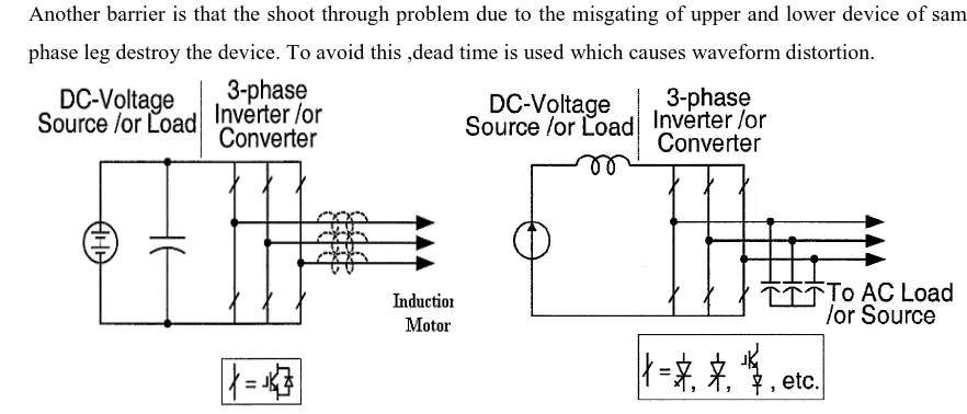
Power electronic inverters are increasingly being used in modern energy conversion systems, including uninterruptible power supplies, motor drives and active interfaces for localized and distributed generation. Voltage source (VSI) and current source inverters (CSI) are the basic traditional power inverters.
Fig. 1 shows the voltage source inverter. In VSI, a DC voltage source is supported by a large capacitor and a 3 phase inverter is used. Despite of wide applications VSI has some limitations:
The output of VSI is always less than input DC and act as a buck inverter. For application where high
output voltage is required with limited DC, a dc-dc boost converter is used .This additional converter stage lowers the efficiency and increases the cost of the system.
Another barrier is that the shoot through problem due to the misgating of upper and lower device of same
phase leg destroy the device. To avoid this ,dead time is used which causes waveform distortion.
Fig. 2 shows the current source inverter. It consist of current source in series with an inductor. However the CSI has also some limitations:
In CSI the input DC voltage is always less than the output voltage and act as a boost inverter .For wide
range application an additional dc-DC buck converter is required. This also increases the system cost and reduces efficiency.
In CSI to avoid the dc inductor to be open circuited at least one of the upper and one of the lower device has
to be gated ON simultaneously. An additional overlap time is needed to achieve this target on the cost of waveform distortion.
The conceptual and theoretical barriers of voltage source and current source inverter can be overcome with an impedance source inverter. This paper describes the operating principle, circuit analysis and control method for the Z-source inverter through simulation by MATLAB.
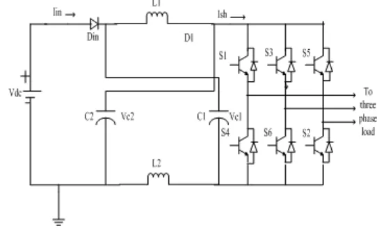
II. Z-SOURCE INVERTER
The new impedance-source power inverter has been recently invented, eliminates all problems of the traditional Voltage source and Current source inverters. The Z-source inverter consists of a unique impedance network
which couple the converter main circuit to the power source, load, or other converter, for providing unique features that cannot be observed in the traditional VSI and CSI inverters. The configuration of three phase Z-source inverter is shown in Fig.3. The input power Z-source is a dc voltage Z-source Vdc that is applied to the Z-Source inverter through reverse blocking diode Din. It consists of two inductors L1, L2 and two capacitors C1, C2
connected in cross coupled shape.
Fig. 3 Z Source Inverter
2.1 Operating Principle
Table. ISwitching Sequence of ZSI
Switching States ( output voltage) S1 S4 S3 S6 S5 S2
Active states{100}(finite) 1 0 0 1 0 1 Active states{110}(finite) 1 0 1 0 0 1 Active states[010}(finite) 0 1 1 0 0 1 Active states{011}(finite) 0 1 1 0 0 1 Active states{001}(finite) 0 1 0 1 1 0 Active states {101}(finite) 1 0 0 1 1 0 Zero states {000} (0V) 0 1 0 1 0 1 Zero states {111} (0V) 1 0 1 0 1 0 Shoot Through states E1(0V) 1 1 1 0 1 0 Shoot Through states E2(0V) 1 0 1 1 1 0 Shoot Through states E3(0V) 1 0 1 0 1 1 Shoot Through states E4(0V) 1 1 1 1 1 0 Shoot Through states E5(0V) 1 1 1 0 1 1 Shoot Through states E6(0V) 1 0 1 1 1 1
The first six states are known as active state. In this the DC voltage is impressed across the leg. Next two
states are null states when the load terminal are shorted through either the upper or lower three devices, respectively.
Last seven shoot through state can be generated when the load terminals are shorted through both the upper
and lower devices of any one phase leg, any two phase leg or all the three phase leg. This shoot through state proved the buck-boost feature to the Z source inverter
2.2 Circuit Analysis
The circuit analysis of ZSI works on the two modes, non-shoot- through mode (active and null state) and shoot through mode (shoot through state). Assuming that the Z–source network is symmetrical i.e. inductors L1 and L2
and capacitor C1 and C2 have the same inductance L and capacitance C.
1 2
L L L
v
v
v
(1)1 2
C C C
v
v
v
(2)2.3.1Nonshoot Through State
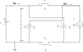
The equivalent circuit of the ZSI viewed from the DC link when the inverter bridge is in one of the eight non-shoot-through switching states is shown in Fig. 4.
Iin Ish
+
-2
C
V
dc
V
1 L
2 L
1 C 2
C
+
+ +
-1
L
v
2
L
v
i
V
2
C
The inverter bridge is in non-shoot-through state for an interval T1, during switching cycle T.
Applying KVL
L dc c
V
V
V
(3)i dc
V
V
(4)PN C L
v
V
v
(5)2
PN C dc
v
V
V
(6)2.3.2 Shoot Through State
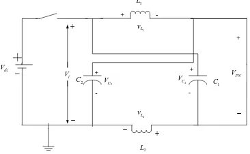
The equivalent circuit of the ZSI viewed from the DC link when the inverter bridge is in shoot-through zero state is shown in Fig. 5.
+ -2 C V dc V 1 L 2 L 1 C 2 C + + + -1 L v 2 L v i V 2 C V PN V
Fig. 5. Operating State at Mode 2: Shoot Through
In steady state the average voltage of the inductor over one switching cycle should be zero, from (3) and (7)
1
(
dc C)
0( )
cL
T V
V
T V
V
T
(10) Or 1 1 0 CT
V
T
T
(11)Similarly the average DC link voltage across the inverter bridge can be found as follows
1
(2
C dc)
0(0)
PN
T
V
V
T
V
T
(12) Or 1 1 0PN dc c
T
V
V
V
T
T
(13)The peak DC link voltage across the inverter bridge is expressed as
1 0
2
PN c L c dc dc
T
v
V
v
V
V
V
T
T
PN dcv
BV
(14) Where 1 01
1 2
T
B
T
T
D
is the boost factor and0
T
D
T
2
PN ac
v
v
M
(15)Where M is the modulation index.
On substituting the value of
v
PN ,
v
ac can be expressed as
2
dc ac
V
v
MB
(16)or
2
dc ac B
V
v
B
(17)Where
B
Bis the buck-boost factor or the gain G.The output voltage can be buck-boost by choosing appropriate value of M and B, the value of B can be controlled by the shoot through duty ratio D.
III.
PWM
CONTROL
FOR
THE
ZSI
How to insert the shoot-through state is the key point of control method for ZSI. For this purpose a modified pulse width modulation control known as Simple Boost Control is used.
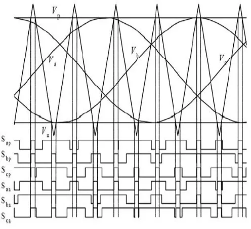
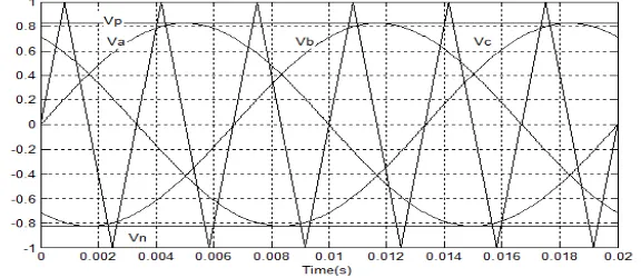
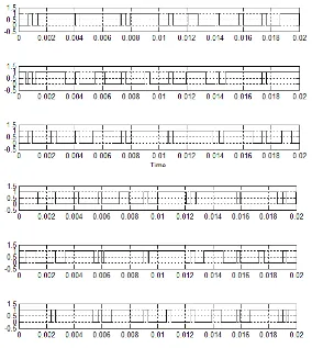
In simple boost control the shoot through is inserted with the help of two straight lines, Vp & Vn. Where Vp and Vn is the positive and negative peak value of three phase sinusoidal references When the triangular wave is greater than Vp or lower than Vn the inverter will operate in shoot-through state ,otherwise operate as traditional inverter.Fig 6 shows the simple boost control method to provide the shoot through in Z Source inverter.
Fig. 6. Simple Boost control
The relation between shoot through duty ratio and modulation index is expressed as:
0
(1
)
T
D
M
T
1
1
1 2
2
1
B
D
M
(19)
2
1
M
G
MB
M
(20)IV.
SIMULATION
RESULTS
To verify the validity of analysis a simulation model is designed. In the simulation all the components are ideal. Table II provides a list of simulation parameter for ZSI.
Table Ii Simulation Parameters of The Zsi
Input DC voltage (Vdc) 100 V
Inductors (L1= L2) 1mH
Capacitors (C1=C2) 1000µF
Switching frequency (fs) 10kHz
Filter inductor ( Lf) 1mH
Filter Capacitors (Cf) 20 µF
Three phase resistive load 10Ω/phase
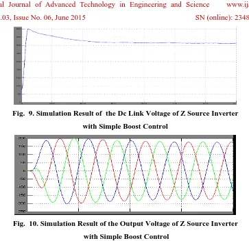
To produce the output line to line voltage of 208 Vrms from the 100 V input DC voltage with simple boost
control for the ZSI, according to (20), M=0.5865.Thus from the above analysis we obtain
(1
)
0.4135
D
M
1
5.78
1 2
B
D
3.39
G
MB
1
1 0
337.28
c PN dc
T
V
V
V
V
T
T
169.5
2
PN ac
v
v
M
V
Fig. 7. Simulation Result of Simple Boost Control
Fig.8 shows the output voltage of traditional voltage source inverter under the same input voltage 100V and modulation index of 0.5865. Thus from the calculation
29.325
2
dc ac
V
v
M
V
Fig. 8. Simulation Result of the Voltage Source Inverter Using the
Traditional PWM Control
Fig. 9. Simulation Result of the Dc Link Voltage of Z Source Inverter
with Simple Boost Control
Fig. 10. Simulation Result of the Output Voltage of Z Source Inverter
with Simple Boost Control
V.CONCLUSION
This paper has presented an impedance source inverter that can produce an output voltage greater than the input by controlling the boost factor. This feature is not possible with the traditional inverters. To achieve this, a modified PWM control method is employed with inverter system. The ZSI can be widely used in photovoltaic application where a low input dc voltage is inverted to high output ac voltage.
REFERENCES
[1] K. Thorborg, Power Electronics. London, U.K.: Prentice-Hall Interna-tional (U.K.) Ltd., 1988. [2] M. H. Rashid, Power Electronics, 2nd ed. Englewood Cliffs, NJ: Pren-tice-Hall, 1993.
[3] N. Mohan, W. P. Robbin, and T. Undeland, Power Electronics: Con-verters, Applications, and Design, 2nd ed. New York: Wiley, 1995.
[4] A. M. Trzynadlowski, Introduction to Modern Power Elec-tronics. New York: Wiley, 1998.
[5] B. K. Bose, Modern Power Electronics and AC Drives. Upper SaddleRiver, NJ: Prentice-Hall PTR, 2002. [6] P. T. Krein, Elements of Power Electronics. London, U.K.: OxfordUniv. Press, 1998.
[7] W. Leonard, Control of Electric Drives. New York: Springer-Verlag,1985.
[8] R. E. Tarter, Principles of Solid-State Power Conversion. Indianapolis,IN: Sams, 1985.
[9] R. D. Middlebrook and S. Cuk, Advances in Switched-Mode Power Conversion.Pasadena, CA: TESLAco, 1981, vol. I and II.