DESIGN AND ASSESSMENT OF FABRY-PEROT
QUANTUM WELL ELECTROABSORPTION
OPTICAL M ODULATORS
A thesis by
Paraskevi Z ouganeli
submitted to the University of London for the degree of Ph.D.
Department of Electronic and Electrical Engineering University College London
ProQuest Number: 10609074
All rights reserved
INFORMATION TO ALL USERS
The qu ality of this repro d u ctio n is d e p e n d e n t upon the q u ality of the copy subm itted.
In the unlikely e v e n t that the a u th o r did not send a c o m p le te m anuscript and there are missing pages, these will be note d . Also, if m aterial had to be rem oved,
a n o te will in d ica te the deletion.
uest
ProQuest 10609074
Published by ProQuest LLC(2017). C op yrig ht of the Dissertation is held by the Author.
All rights reserved.
This work is protected against unauthorized copying under Title 17, United States C o d e M icroform Edition © ProQuest LLC.
ProQuest LLC.
789 East Eisenhower Parkway P.O. Box 1346
ABSTRACT
The optical properties of m ultiple q u an tu m w ell (MQW) m aterial can be modified by application of an electric field across the wells. Hence, by locating the wells in the intrinsic region of a p-i-n diode, an optical beam incident on the diode m ay be m odulated. The incorporation of such a diode in an integrated Fabry-Perot (FP) cavity yields an enhancem ent of the m odulation characteristics. This thesis deals w ith the assessm ent an d o p tim isation of Fabry-Perot reflection m o d u la to rs in the G aA s/A lG aA s material system, w here the electroabsorption effects in quantum wells are employed to attain voltage-controlled optical intensity modulation.
The w ork is prim arily concerned w ith the asym m etric Fabry-Perot m odulator (AFPM) w here the front m irror of the FP cavity is of low er reflectivity than that of the back. A lthough the achievable very high onroff reflectivity ratios m ake this type of device very attractive, its ultim ate im plem entation im poses a n u m b e r of o th er requirem ents. Firstly, the operation needs to be com patible w ith existing electronics req u ired to drive the m odulator. Secondly, the perform ance m u st be to leran t to fluctuations of a num ber of param eters associated both w ith the epitaxial grow th and w ith the operational conditions including am bient tem perature. O u r optim isation aims, therefore, both to im prove the m odulation characteristics and to m aximise the tolerance of the structure. To do this, we examine theoretically and experim entally the param eters that affect the perform ance, addressing both the qu an tu m well effects and the m icroresonator design. We develop a com prehensive design m ethod, dem onstrate m odulators w ith im proved characteristics, proceed to a thorough evaluation of the perform ance ultim ately attainable by AFPMs, and finally produce optim ised designs to meet predefined specifications.
A nother quantum well electroabsorption-based device, the sym m etric cavity electroabsorption m odulator (SCEM), is fully investigated a n d its relative m erits are critically examined. In this case the front and back m irrors are equal an d the device offers certain advantages in the norm ally-off mode, thereby lending itself to optically bistable operation. W e dem onstrate sw itching using SCEMs in the sym m etric self- electro-optic-effect device (S-SEED) configuration.
LIST OF CONTENTS
ABSTRACT... 3
U S T OF CO NTENTS...4
Chapter
1: INTRODUCTION 1.1 Historical developm ent... 91.2 Optoelectronic system s... 11
1.3 Q uantum wells (QW) 1.3.1 Quantum well effects...16
1.3.2 Quantum well modulators... 21
1.4 Q uantum well m odulators in optoelectronic logic...24
1.5 Introduction to the thesis... 27
Chapter
2: THE INTEGRATED FABRY-PEROT MODULATOR: OPERATION, DEVICE FABRICATION, EXPERIMENTAL METHOD, AND OPTIMISATION OBJECTIVES 2.1 Introduction... 312.2 The Fabry-Perot effects... 32
2.3 The integrated Fabry-Perot m odulator 2.3.1 Principles of operation... 34
2.3.2 Experimental performance... 36
2.3.3 The electrorefractive effects... 40
2.3.4 The multilayer reflector stack... 42
2.3.5 Epitaxial growth and device fabrication... 46
2.3.6 Device speed... 49
2.4 Experimental testing ap p aratu s...51
Chapter
3: MODELLING OF FABRY-PEROT ELECTROABSORPTION DEVICES3.1 Introduction...57
3.2 M odelling of a multilayer device... 58
3.3 M odelling of the MQW absorption spectra...62
3.3.1 The tunnelling resonance technique... 63
3.3.2 Scaling to experimental absorption spectra... 66
3.3.3 Evaluation of the field-dependent spectra... 69
3.3.4 Lifetime-related lineshapes (Homogeneous broadening)... 73
3.4 Com parison w ith experiment...77
Chapter 4:
THE TEMPERATURE TOLERANCE OF THE ASYMMETRIC FABRY-PEROT MODULATOR 4.1 Introduction... 864.2 The effect of tem perature on the Fabry-Perot m odulator...87
4.3 Experimental study of the tem perature sensitivity of CB145 4.3.1 Experimental set-up... 90
4.3.2 Experimental spectra with varying temperature... 91
4.3.3 Fixed wavelength operation... 94
4.3.4 Tracking the optimum operating wavelength... 98
4.3.5 Self-linearised operation... 102
4.4 Discussion and Sum m ary... 104
Chapter
5: TOLERANCES OF THE ASYMMETRIC FABRY-PEROT MODULATOR 5.1 Introduction... 1085.2 Tolerances to grow th inaccuracies 5.2.1 Growth calibration... 109
5.2.2 Lateral uniformity... 112
5.2.3 Relative merits of growth processes regarding lateral uniformity...118
5.2.4 Post-growth compensation for lateral non-uniformity... 121
5.3 Combined tolerances 5.3.1 High contrast modulation... 122
5.3.2 Large reflection change modulation... 131
5.4.1 Optical addressing of two-dimensional arrays
of modulators... 141
5.4.2 Effect of the optical angle of incidence... 143
5.4.3 Tolerance to the angle of incidence... 148
5.5 Conclusions
Chapter 6:
TRADE-OFFS INVOLVED IN THE AFPM PERFORMANCE IMPOSED BY THE MIRROR DESIGN 6.1 Introduction... 1536.2 The Fabry-Perot cavity design...154
6.3 Experim ental confirmation of the effect of the FP cavity design u p o n the m odulator perform ance 6.3.1 QT131 A F PM... 158
6.3.2 Q T223A F P M... 162
6.4 C onclusions...168
Chapter 7:
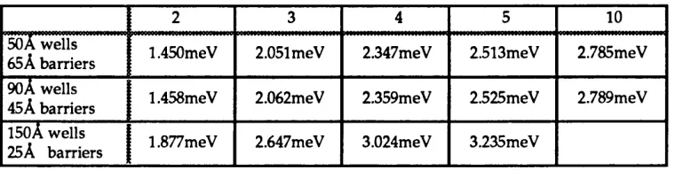
ASYMMETRIC FABRY-PEROT MODULATOR DESIGNS 7.1 Introduction... 1707.2 D eterm ination of the m inim um barrier w id th ... 171
7.3 Detailed stu d y of trade-offs...175
7.4 Specific norm ally-on AFPM designs... 186
7.5 Conclusions...191
Chapter
8: THE SYMMETRIC CAVITY ELECTROABSORPTION MODULATOR 8.1 Introduction... 1948.2 O peration of the symmetric cavity electroabsorption m odulator (SCEM)... 195
8.3 Experim ental results 8.3.1 QT153 SCEM... 200
8.3.2 Q T280B SC EM... 205
8.4 Further discussion: Tolerances of the SCEM... 210
8.5 A pplication of SCEMs in SEEDs 8.5.1 Normally-off AFPMs: Performance limitations... 213
8.5.2 SCEMs in SEEDs... 217
Chapter 9:
APPLICATIONS OF THE FABRY-PEROT MODULATOR AT THE CHIP LEVEL9.1 Introduction...226
9.2 Integration 9.2.1 General... 227
9.2.2 Integration with electronics... 229
9.2.3 The integrability of the Fabry-Perot modulator... 232
9.3 Proposed applications of Fabry-Perot m odulators in com posite devices...236
9.4 Sum m ary...242
C O N C LU SIO N ...245
ACKNOW LEDGEM ENTS... 248
APPEN D IX : DETAILS ON MODELLING... 250
REFERENCES... 255
PUBLICATIONS... 277
-CH A PTER 1: INTRODUCTION
1.1 HISTORICAL DEVELOPMENT
The invention of the transistor in 1948 signifies th e startin g -p o in t of the contem porary technology oriented period th at has earned the title: inform ation era. Since the 50's, th ere has been a steady exponential ad vancem ent in electronics predom inantly d ue to the fast-paced progress in sem iconductor technology and in particular the integration of th o usan d s of different com ponents in light, com pact, sm all-area chips. Indeed, the m ost valued craft of the last q u arter of the century has been m iniaturisation. The im pact of these advancem ents has been trem endous in an intriguing range of w ays, indeed it can be said that m ost of the progress in other sciences, from medicine to astrophysics, has by and large been a bi-product of the vast and diverse achievements in the electronics industry that facilitated better diagnostics and accurate instrum entation. Inform ation exchange and processing are in intim ate relation w ith the very fabric of the current social-economic structures. The increasing dem and for high speed large throughput inform ation technology has so far been met by an increase of com ponent density and a sim ultaneous enlargem ent of chip area. It has, however, been realised that there are some fundam ental lim its to the perform ance that can be attained by electronics, as they are limited by p ropagation delays on the capacitive connectors. A dditionally, the area of telecom m unications has suffered substantial lim itations d u e to high transm ission losses a n d restricted b a n d w id th availability, which have been alleviated by the im plem entation of the optical fibre.
c u rre n tly ach iev ed c o st/p e rfo rm a n c e fig u res e stab lish in g its d o m in a n c e in telecommunications. Indeed, fibres are now extensively used in sub-m arine system s and are generally the preferred m edium for long-haul communications. Furtherm ore, the developm ent of Er+ d o p ed fibre am plifiers has resu lted in v irtu ally lossless transm ission links. This has encouraged further dem ands for broadband services.
As the technologies m ature and at the sam e time it becomes clear that optics is here to stay, it is evident that there m ay be a m uch m ore substantial role optics can play. Optics offers a vast available bandw idth, m assive parallelism , and high speeds, an d hence it m ay prove a viable solution to problem s encountered in inform ation technology in the broad sense, i.e. be it telecom m unications or connections betw een m odules in a data processor. O ptical interconnects can be u sed w ith in processing system s to alleviate the speed and capacity lim itations in VLSI. As this h as been broadly investigated, new issues have been revealed w here a certain d eg ree of functionality of the optical node, other than that of a m ere interface elem ent, appears possibly advantageous. A dditionally, as transm ission becom es less of a n issue, problem s encountered at the sw itching end of fibre com m unications p ro m o te the notion of switching being perform ed in the optical dom ain. Thus, progressively, optics is being considered for possible im plem entation higher u p the hierarchy of data m anipulation. The degree to which this m ay materialise is in m any areas still open to debate.
realisation of a ran ge of very efficient optoelectronic dev ices w hich co m p are favourably to these in bulk material. Such devices in GaAs are strong candidates for several applications in optical interconnection an d switching netw orks. O n the other hand, InP based material is used in long-haul com m unications in order to exploit the low-loss w indow of the optical fibre (=1.55|im).
This thesis is concerned w ith a class of G aAs m u ltip le q u a n tu m w ell optoelectronic devices w here the reflected optical in ten sity is controlled by the electrical signal applied to the term inals of the device. Specifically, we are concerned w ith Fabry-Perot q u an tu m w ell electroabsorption m odulators in the GaAs m aterial system. W hen this w ork w as started such m odulators, nam ely th e asym m etric Fabry- Perot m odulator, had just been dem onstrated [W hitehead et ah, 1989b; Yan et a l, 1989] w ith m odulator characteristics that clearly outperform ed other sem iconductor such devices. The aim of this w ork w as to study such devices in greater detail and optimise their performance. Such optical m odulators m ay become im portant elements at the interface betw een optics and electronics th at lend them selves to a variety of functions in optoelectronic systems. It was decided that the direction of this w ork w ould be tow ards a realistic evaluation of the potential for im plem entation of this type of m odulator in a real system and thus its perform ance o u g h t to be stu d ied and optimised w ith real conditions and systems requirem ents in m ind.
In the following w e give a brief account of optoelectronic system s considering in particular areas w here the reflection m odulator m ay be incorporated. Subsequently, after an introduction to quantum well effects, we present the m ain types of m odulators that may be realised using quantum well material and which can be used as building blocks in m ore com plex com posite structures. Finally, w e in tro d u ce briefly the implem entation of composite quantum well devices in optoelectronic logic.
1.2 OPTOELECTRONIC SYSTEMS
A w id e ra n g e of o p to electro n ic sy stem s h as b e e n d e v e lo p e d for communications, interconnection, optical com puting, neural netw orks, as well as for applications in industries not directly associated w ith inform ation technology. From these, the systems at the com m unications end of the range are at the m ost advanced stage as their im plem entation is imminent. A discussion of optoelectronic system s in
-general is certainly beyond the scope of this introduction. In this section w e give, therefore, a brief account of systems from the perspective of potential applications for a sem iconductor reflection m odulator.
Optical interconnects in VLSI
Faster processing of ever larger am ounts of data has been achieved by scaling dow n the device features in ICs a n d a sim u lta n e o u s scalin g u p of th e chip-size. C onsequently, the density of devices p e r u n it chip area is increased, the pow er dissipation p er device is decreased an d so is the sw itching delay of each gate. The interconnect RC time, how ever, rem ains u nchanged [G oodm an,1984], w h en at the sam e tim e the enlarged chip size results in a larger num ber of elem ents p er block and thus m ore an d m ore interconnects betw een blocks. F urtherm ore, as clock speeds increase, clock skew s are caused by the different p ath delays along v ary in g path lengths [M idw inter, 1988]. The situ atio n has th u s reached th e stage w h ere the p erform ance is in fact in m an y cases I n p u t/O u tp u t (I/O ) b o u n d ra th e r than processing bound. To take this argum ent a bit further, current electronic technologies are certainly poor in supporting the necessary I /O density and bandw idth required for large am ounts of data and parallel com puting [Feldman, 1990; G uha et a l ,1990]. In the course of various developm ents in optics there has been a certain advancem ent in the perform ance of electronics in recent years. An attem pt to minimise the interconnection lengths and achieve better overall chip-topography has been the im plem entation of m ulti-layered chips w here m any levels of interconnections are stacked together in the vertical direction w ith p o in t connections joining layer to layer [Topham , 1991]. How ever, these circuits suffer severe heat dissipation problems.
O ptical interconnects offer th e p o te n tia l to overcom e th e lim itatio n s encountered in VLSI im plem entations and yield faster point-to-point com m unications with a reduction of the necessary electrical pins p e r chip. This can result in designs that consum e less pow er, an d operate at higher speeds. A dditionally, the footprint area corresponding to the "optical p ads" is reduced as com pared to electrical pads that norm ally occupy =25% of the chip area. The 'break-even' length w hen com paring optical and electrical interconnects in term s of pow er consum ption has been estim ated to a couple of m m beyond w hich optics is m ore efficient than electronics. This is, nevertheless, very m uch d e p en d e n t u p o n the specific com ponents as w ell as the application [Farhadiroushan et a l, 1991]. Also one can argue that pow er consum ption is only one of the points to be considered.
distance system s, G aAs based m aterial could be fav o u red as stem m in g from its sup erio r perform ance. The approaches tow ards optical interconnects in VLSI m ay be classified in tw o types: guid ed and free-space interconnects. The form er could be im plem ented using for example polym er w aveguides in the backplane [Guha et ah, 1990] or other w aveguides and optical fibres [Goodman, 1984] for connections betw een various levels. Free space interconnections of VLSI im plem entations allow for direct access to various locations on the chip and are inherently flexible to ultim ately offer the possibility of dynam ic reconfiguration of the connecting routes betw een elements.
Holographic Element
vW
Electronic
Island modulators
\ \ \
detectors
1
F i g . 1 . 2 .1 A schematic diagram illustrating the use of reflection modulators as optical pads performing the connections between islands of electronics in VLSI. Diagram not to scale.
H olographic elem ents m ay be used to facilitate complex connectivity. These w ould be preferably com puter generated as it w ould be uneconom ical to realise an optically generated hologram in cases w here dense complex routing is required [Facanha et a l, 1989].
The transm itter elem ent m ay be either a laser d io d e or a m odulator. In the case of free-space interconnections, m odulators seem ed at the start of this w ork to be the m ost viable candidate since the perform ance of surface emitting diodes was simply inadequate. H ow ever, the advancem ents in surface em itting laser diodes in the last five years [see for exam ple Yoo et ah, 1990; O renstein et ah, 1991] have prom oted th em to serio u s c a n d id a te s for 2-D a rray s of tra n sm ittin g elem ents in these im plem entations. H ow ever, there are two major disadvantages encom passed w ith the
w o r e use of lasers for this task [M idwinter, 1987]. One is that lasers are very m u c h Apow er consum ptive devices an d this w ould inhibit the realisation of high-density netw orks w ith optical m odules integrated in close proxim ity to the electronic ones. A second disadvantage is that lasers are devices critically dependent u p o n the epitaxial m aterial quality and the operational conditions. Therefore, for exam ple, it w o u ld be quite difficult to realise reliable lasers in GaAs m onolithically integrated on Si electronics
-(C hapter 9). In addition to the above argum ents, the u se of m o d u lato rs offers the advantage that the optical source is located aw ay from th e active chip an d thus not only dissipates its heat elsewhere bu t also facilitates better tim ing and control of the elements [Midwinter, 1987]. Finally, and very im portantly, a m odulator can com prise the m ain element of both the transm itter and the receiver end of the link. The created bi-directional paths can offer ad d itio n al connectivity, flexibility, a n d u ltim ately dynam ic reconfigurability. Thus one could envisage arrays of reflection m odulators acting as the interconnecting p ads betw een electronic islands or betw een boards in free-space links (Fig.1.2.1) [see Parker, 1991].
Optical switching
At present transmission rates in fibre optic packet switching system s routing decisions can be m ade electronically, thus hybrid architectures are used w here the transm ission is done optically and the switching electronically. H ow ever, as the transm ission rates increase electronic processing will find it increasingly difficult to perform the required ro u tin g functions. The electronic sw itch suffers from relatively low transm ission bandw idths while also the optoelectronic (O /E ) interfaces associated w ith the hybrid architectures prevent the full exploitation of the large bandw idth-distance product of the optical fibre. To fully exploit the advantages of optics, it w ould be desirable to generate, transmit, process, and detect broadband high frequency optical signals in the optical dom ain and interface these to external, probably Si based, integrated circuits operating at the sam e speed. Thus the possible data flow bottleneck created at the electronic switch w ould be overcome.
Switches m ay be realised using either logic devices or u sin g passive devices that respond to some routing instruction, be it in the time or the w avelength dom ain [M idw inter, 1988]. The latter (i.e. relational switches) w o u ld have th e a d d itio n al advantage of a versatile ban d w id th provided by the "tran sp aren t" sw itched optical path. That is, unlike an electronic sw itch w hich operates for a certain type of data form at, an optical switch m ay be able to cope w ith any optical signal p rov id ed of course this lies w ithin a certain w avelength range. Thus in total, the u se of optical sw itching w ould realise system s that take full advantage of the endem ic qualities of optics: parallelism, broad bandw idth, and high speed. From a historical perspective, sw itching has alw ays followed the form at of transm ission [N ussbaum , 1988], and transm ission is now being perform ed increasingly in the optical dom ain. There is, how ever, a series of practical difficulties th a t m u st be b y p assed before optical switching is actually implemented.
m akin g u se of a b so rp tio n o r p h ase tech n iq u es, all-o p tical b istab le devices, sem iconductor optoelectronic logic. A review of sem iconductor-based sw itches has been presented by Ikegami [1988], while several approaches have been realised in the laboratory since then [see for example Lindgeren et al., 1990; Shim om ura et a l, 1992;
N Inputs
CrossBar Switch
N Outputs
Fig.1.2.2 A schematic diagram showing the connection of N inputs to N outputs using a crossbar switch. A matrix ofN xN elements is required.
H am am oto et al., 1992]. Self-routing switches, i.e. switches th a t can decide u p o n the function to apply at the in p u t signal as this is dictated by a h e ad e r in stru ctio n preceding the signal, have received much interest [Ballance et al., 1990]. Such switches perform the switching action w ithout needing to know the inputs to the other ports to the netw ork, thereby resulting in faster processing. Self-routing electronic sw itching n etw orks are m ainly lim ited by I /O capacity. H ence o ptics could be u se d in conjunction w ith electronic switching in a less am bitious m anner, to constitute the I /O elem ent between islands of electronic logic (J.E. M idwinter, private communications).
The role of optical switching m ay also be envisaged in data processing as the im plem entation of optical interconnection m ight favour the addition of a certain level of intelligence in the elem ents that perform the connection. In the sim plest form of a switching net the pixels act merely as shutters that m ay or m ay not transm it the optical signal. In m ore com plex array s, each pixel m ay p e rfo rm b o th d etectio n an d transm ission and, m oreover, apply some logic function before transm itting. These so called "sm art-pixels" [see for example K urokaw a et a l, 1992; M idw inter, 1988] could assist in achieving such levels of v ersatility an d com plex fu n ctio n ality th at fundam entally new routes in signal processing and d ata m an ip u latio n could be opened. Electronic com ponents w ould be part of the intelligence. The extent to which these w ould be incorporated w ithin the node is an oth er issue to be ad d ressed , as
15-functionality m ay start decreasing again after a certain level of electronics have been incorporated in the node.
Interconnections are an inseparable p art of sw itching netw orks. Bus, crossbar, and (possibly 3-D) m ultistage architectures can b e utilised [Kiamilev et al., 1991]. The two form er have a lim ited I /O capacity while, in the case of a 3-D m ultistage netw ork (such as a shuffle or butterfly net), the exploitation of the second dim ension in the in p u t and the o u tp u t plane allows large am ounts of d ata to be m an ip u lated [Taylor an d M id w inter, 1991]. For co m m u n icatio n s a p p lic atio n s a c ro ssb a r n etw o rk connecting N=128 or 256 in p u ts to an identical n u m b e r of o u tp u ts (and hence requiring a N xN num ber of nodes) is the type of sw itch that could be im plem ented in the n e ar fu tu re [M idw inter, 1987]. O n th e o th e r h an d , in n o n -com m unications applications, in the case of a parallel co m p u ter eg., m ultistage n etw o rk s could be preferred in som e cases as they provide efficient perform ance u sin g a reasonable num ber of switches [Guha et a l, 1990; M atsuda and Shibata, 1991].
1.3 QUANTUM WELLS
1.3.1 Q uantum well effects.
The term quantum well m aterial refers to a class of sem iconductor m aterial w here tw o sem iconductors of different band g ap s are san d w ich ed together so that electrons and holes experience a potential well in the conduction and the valence band respectively in the direction perpendicular to the plane of the layers. W hen the w id th of the w ell is less than *200A, confined states are created for the carriers in the sem iconductor w ith the low er ban dg ap energy (well) (Fig.1.3.1). The situation is a bit m ore com plicated in the valence band w here the confinem ent lifts the degeneracy at the centre of the band since the effects are dep en d en t u p o n the m ass of the particle involved (Appendix). This leads thus to separate hole-bands at k=0, i.e. the light hole and the heavy hole (Chapter 3). Transitions m ay take place betw een the discrete levels created in the conduction and the valence band w ith the low est transition occurring at an energy higher than the corresponding band-gap.
3-D to a step function in the case of qu antu m wells (Fig.1.3.2). The steps correspond to the n=l,2,... levels. At the sam e tim e the confinem ent of the carriers w ith in the well results in tighter-bound excitons, i.e. hydrogen-like b o u n d electron-hole pairs. Thus, unlike bulk, th e excitons in q uan tu m wells are not ionised at room tem p eratu re as their binding energy is now greater. Excitonic features are observed in the absorption spectra as sharp peaks at an energy equal to the sub-band energy m inus the binding energy of the pair. In total, the absorption spectra of quantum wells exhibit a step-like shape w ith the excitonic features superim posed at the edge of each step a n d the sam e features are th u s observed in the p hotocurrent spectra obtained from a p-i-n such stru c tu re (Fig.1.3.2). These features n o t only increase the ab so rp tio n coefficient c o m p a re d w ith th a t of b u lk m a te ria l, b u t also g ive rise to p ro n o u n c e d electroabsorptive and electrorefractive effects that lend themselves to efficient voltage- induced m odulation. W e discuss this later in this section.
The advancem ent in epitaxial grow th technology has allow ed the realisation of G aA s/A lG aA s quantum wells. The first observation of quantisation effects w as by D ingle and co-w orkers in 1974 at liquid helium tem p eratu res (4K). F u rth er rapid im provem ent in epitaxial grow th techniques has perm itted the achievem ent of sm ooth interfaces and of good control of the layer thicknesses [Herman et a l, 1991] so that
AlGaAs GaAs AlGaAs
_ hh2 • - Ih2
Conduction Band
Valence Band
Fig.1.3.1 Quantum wells are formed when alternating layers of typically **100A GaAs and AlGaAs are sandwiched together. These are formed perpendicular to the growth direction (z). Confined states (n=l,2 shown) for the electron (en) and for the heavy- and light-hole (hhn and Ihn) occur
within the well (type I). The fundamental transition corresponds to E c v as opposed to the smaller band-gap energy E .
o
-3D
2D
P hoton Energy
600
AlCaAs absorption
edge I
500
e2-hh2 e l- h h l
400
e l- lh l 300
200
100
0
1.5 1.7 1.8
1.4 1.6
Photon Energy (eV)
Fig.1.3.2 The top graph is a schematic of the parabolic density of states corresponding to the 3D bulk case, and the step like DOS corresponding to the 2D case (infinite wells). The bottom plot shows experimental photocurrent data with clear quantisation effects. These have been obtained from a 95A well p-i-n diode at zero Volts (Built-in field).
clear quantisation effects are now routinely observed at room tem perature (Chapters 3 and 5).
Quantum confined Stark effect (QCSE)
an d for zero field, the w avefunctions are orthogonal an d thus only transitions w ith An=0 can take place. In a real quantum well system, the barrier-height is finite leading to a deviation of the w avefunctions from sim ple sines an d cosines and a considerable penetration into the barrier. This causes a partial break dow n of th e selection rules even in the zero field case discussed above, b u t n everth eless in th at case only transitions w ith An=0 result in pronounced features (Fig.1.3.2). U pon the application of a field perpendicular to the plane of the wells, the shape of the well changes and as a result the energy levels w ithin the well are altered. The transitions occur a t sm aller energies and thus the excitonic features red-shift. The application of a field causes the
G aA s
AlGaAs
30000
hh 14kV/cm
83kV/cm § 25000
i j 20000
0 15000 £
.2
i o o o o1
| 5000
<
hh
el-hh2
820 840 860 880
W avelength (nm)
Fig.1.3.3. Upon the application of an electric field perpendicular to the plane of the wells, the well is tilted and the energy levels shift to longer wavelengths. This is manifested in the experimental absorption spectra of a 95 A. The el-hhl (hh) and el-lhl (Ih) transitions subside with field, while the "forbidden" el-hh.2 is gradually enhanced with field.
19-selection rules to break completely as the sym m etry along the m id d le of the w ell is destroyed and the wavefunctions lose their parity. At the sam e tim e, the tw o carriers are pushed to opposite sides of the well as a result of the opposite electrical forces they experience. These tw o effects lead to a reduction of the overlap betw een the tw o w avefunctions for an "allow ed" transition a n d an increase for several previously "forbidden" transitions. In total, the m ain excitonic features in the absorption spectra red-shift w ith the application of a field, at the sam e tim e g rad u ally losing th eir strength as the field is increased (Fig.1.3.3). W e discuss this in som e detail in C hapter 3. The QCSE w as quantified and explained by D.A.B. Miller [1984], w hile the first people to observe the QCSE-associated red-shift of the spectra w ere Chem la and co-workers [1983]. A neat w ay to m ake use of the effect is to incorporate the wells in the intrinsic region of a p-i-n diode, as w as first done by W ood and co-w orkers [1984]. All the above observations w ere first m ade in GaAs w hile now different m aterial system s h av e been successfully realised. Finally, it is im p o rta n t to n o te th a t th e electroabsorptive effects are sim ultaneously accom panied by stro n g ly w avelength d ependent electrorefractive effects as the tw o param eters (i.e. the absorption and the real index) are intimately interrelated (Chapter 2).
1.3.2. Q uantum well m odulators.
The w orldw ide research in QWs has yielded a large range of optical as well as electronic devices that incorporate this type of m aterial. The optical devices m ay be classified in tw o m ain categories: passive elements, i.e m odulators and detectors, and active elem ents, i.e. lasers lig h t-em ittin g d io d e s a n d o ptical am p lifiers. The perform ance of these devices is m ore than often superior to those of bulk devices. H owever, the prim e advantages of quantum well material lie firstly w ith its versatility in term s of the large diverse range of devices that m ay be fabricated and w hich are, m ore often than not, m utually integrable on the sam e w afer, an d secondly w ith the vast scope for bandgap engineering that yields tailored operation w ithin a large range of wavelengths. In the following w e discuss quantum well m odulators.
Modulators
The strong electroabsorptive an d electrorefractive effects in QW s (Fig.1.3.3) can be exploited to realise voltage-controlled optical m odulation. M odulators fall in tw o classes according to the direction of propagation of the optical beam w ith respect to the plane of the well, referred to as w aveguide and transverse structures (Fig.1.3.4).
W aveguide m odulators: H ere the light propagates parallel to the plane of the wells and the absorption-length product (ad) is determ ined by adjusting the length of the w aveguide. Thus incorporation of a sm all n u m b er of w ells in th e intrinsic region results in low voltages for a given electric field w hile the m o d u latio n d e p th is determ ined by the length of the device. There is, how ever, a trade-off betw een the operating voltage and the operating speed of the devices as th eir capacitance is increased for increasing guide length and decreasing intrinsic w idth. W aveguides are polarisation sensitive devices as the heavy-hole transition is not an allow ed transition for the TM m ode [W eisbuch an d Vinter]. The results of W ood et al. [1985] that achieved lOdB contrast at 15 V w ith an insertion loss of 7.2dB are typical for an electroabsorption-based device in the GaAs system . In general, good contrast ratios may be attained at relatively low voltages w ith such m odulators provided the quality of the quantum well m edium is sufficiently high. H igh speed phase m odulators have also been intensely investigated [M endoza-Alvarez et a l, 1988]. Effects other than the electroabsorption and electrorefraction m ay also be utilised to obtain m odulation. For example, Zuckeref a l [1990] have achieved m odulation by use of a current injection bandfilling m echanism w here the carriers are stored in a (doped) barrier reservoir. Finally, M oretti et a l [1992] h ave d em o n strated 22dB co n trast at 2.5V u sin g a
-superlattice. The insertion loss was, however, 13dB.
W aveguides have received a lot of atten tio n because they are directly integrable w ith conventional lasers and ultim ately also w ith fibres Their im pact in photonic circuits to realise integrated receivers incorporating w avelength- an d time- division m ultiplexing is expected to be very large, although no t necessarily solely in the form of qu an tu m well devices [Walker, 1991]. For these applications, InP based material will have to be used to exploit the low-loss optical w indow in fibres (=1.55|im) [Piitz, 1991].
Transverse m odulators: Both in optical switching and in interconnections applications, it m ay be necessary to fabricate large tw o-dim ensional arrays of devices in o rd er to achieve bigger pin density. This makes transverse devices m ost desirable as they allow free-space direct communication, random placement on a chip, easy access for
MQW
►
Waveguide
J
etched-off substrate
Transmission
coating Mirrors
Double-pass Fabry-Perot
Reflection Reflection
Fig.1.3.4 Various quantum well modulator configurations.
optical accessories, and flexibility in connection routes. These m ay be found in the transm ission or the reflection mode.
a l, 1988]. A serious disadvantage of transm ission m odulators in the GaAs system is that the substrate has to be etched off as it is absorbing at the w avelengths of interest. This, ap art from com plicating the processing, results in b rittle devices. In certain system s the transm ission m ode m ay be beneficial and in particular in the InP system w here the substrate is transparent [Barnes N, 1990a,b]. In general, however, reflection m odulators are preferable as they offer better flexibility in positioning and addressing on a chip. A dditionally, they acquire a better potential for vertical integration w ith electronics as well as w ith other optoelectronic devices.
ii. Reflection m odulators: a)Double-pass reflection: W ith a Bragg reflector at the back and an anti-reflection coating at the front, a double-pass reflection m odulator can be realised. The voltages of operation are half those of the transm ission m odulator for a given intensity change/contrast. A contrast of 9dB has been attained at 18V w ith an insertion loss of 5.7<lBfrom such a structure [Boyd et a l, 1987]. Recently, A m ano et a l [1991] have dem onstrated a double-pass reflection m o d u lato r w ith >20dB contrast. This was achieved by a dram atic reduction of the background doping in the intrinsic region to <1014cm*3 and the incorporation of 220 wells. C onsequently, the operating voltage of th at device is very high at 30V. b)Electrorefraction-based Fabry-Perot m odulator (Symmetric Fabry-Perot m odulator, SFPM): Such m odulators are realised w ith a front and back reflector so that a Fabry-Perot cavity is formed. The resonance of that cavity is set at a w avelength far aw ay (to longer w avelengths) from the zero bias exciton peak to attain a large ratio A n/A a, w here n is the real p art of the refractive index and a is the absorption coefficient. The device is op erated at its u nb iased resonance and is not reflecting at zero bias w hereas w ith a reverse bias applied the change of the index induces a shift of the resonant position. Consequently, a rise of the reflectivity at the position of the initial resonance is accom plished w ith bias. In theory such devices may achieve high contrasts. In practice, how ever, the combined effect of the high finesse and the required good m atching betw een the reflectivities of the grow n m irrors severely limits the m odulation perform ance, an d in particu lar the obtained contrast. M oreover, the operating voltages are inherently high because the operating w avelength is at a large separation from the exciton. Such devices inherently suffer from relatively high insertion losses. C ontrast of 9dB has been exhibited at 25V w ith an insertion loss of 5.8dB [Simes et a l, 1988]. The low optical b an d w id th and the slim tolerances of the SFPM are big disadvantages. c)Electroabsorption-based Fabrv- Perot modulator: Here the electroabsorptive effects serve to reduce the effective back m irror and thus m odulate the overall reflectivity at the resonant w avelength. Such a stru ctu re incorporating u neq u al (asym m etric) m irro rs w as first p ro p o se d and dem onstrated by W hitehead et a l [1989b] an d in d ep en d en tly by Yan et a l [1989].
23-This asymm etric FP m odulator (AFPM) exhibited a record contrast in excess of 20dB at 9V w ith an insertion loss of 3.5dB. M oreover, the w av elen g th range over w hich contrast in excess of lOdB is achieved is =6nm. This device perform ance was a major im provem ent over previously achieved perform ances. It is this type of m odulators that w e are concerned with in this thesis. Since the introduction of the AFPM in 1989, the operating voltage of such devices has been reduced to as low as 3V, in parallel w ith, and as a result, of the w ork presented in this thesis, m aking the device attractive for m any of the applications discussed earlier in this introduction.
1.4 QUANTUM WELL MODULATORS IN OPTOELECTRONIC LOGIC
In order to perform optical logic it is required to either obtain bistability or a transfer characteristic w ith tw o hard limits so as to unam biguously encode the tw o logic levels. V arious optical logic fu n c tio n s m ay th e n b e p e rfo rm ed u sin g combinations of such devices. Ideally the devices should acquire non-critical biasing, in p u t/o u t p u t iso latio n , logic level re sto ra tio n , a n d m u ltip le fu n ctio n ality . A dditionally, high speed operation at low optical p o w er in p u ts, cascadability, and fan-out are vital for digital logic implementations.
There are several technologies that could be used in this respect [M idwinter, 1988]. Liquid crystal devices show bistable operation [Lloyd, 1987] b u t they have the disadvantage of slow speeds (ns). Bistability that relies on non-linear phenom ena in sem iconductors (and indeed as a rule in m ost materials) requires large in p ut pow ers [Sfez et al., 1990] which in principle does no t favour such devices. A class of devices that seem to offer m any of the previously m entioned required characteristics, utilise a combination of electroabsorptive effects and electrical feedback. Thus these devices are not purely optical in nature, although the inputs and the o u tp u ts are all in the optical dom ain, because electrical transport is endemic to their operation. Q uantum wells are incorporated in such structures in m ost cases but som e n on -q u an tu m w ell devices have also been dem onstrated. We refer to these below.
Self-Eledro-optic-Effect-Device (SEED)
identical m odulators connected in series, the symmetric-SEED (S-SEED), is far superior [Lentine et a l, 1988] and thus w e will m ainly discuss the S-SEED. This device m ay be realised w hen the individual m odulators show negative differential resistance (NDR), i.e. a decrease of the cu rren t w ith biasing voltage. NDR is obtain ed for MQW m odulators w hen operating at the vicinity at the zero bias heavy-hole exciton peak (Fig.1.3 .3). W hen the tw o m odulators are connected in series, K irchoff's law s im ply that an increase in the pow er absorbed on D1 (Fig.1.4.1) w ith respect to that absorbed in D2 is projected as a decrease of the voltage that is applied across D1 and vice versa. M oreover, as a result of the NDR, positive feedback is applied th at causes the device w ith the least pow er-input to be it its least absorbing state. The op eratio n is best understood by observing the load lines. A a more detailed account of the exact
(a) (b)
D i
r
D
In p u t vs O u tp u t for D l w ith P2 fixed
AB
out
CD.
m
F ig .1 .4 .1 A schematic showing the connection of two modulators in the S-SEED configuration (a). The performance is symmetrical for the two diodes. With a fixed amount of power incident on one of the diodes, the input-output characteristic of the other exhibits bistability (b).
m echanism is given in C hapter 8 of this thesis. For a certain p air of inputs, there are tw o stable modes of operation provided the tw o pow ers are sufficiently different. One of the diodes is it its absorbing state w ith very little voltage at its term inals, an d the other is it its least absorbing state w ith virtually all the biasing voltage applied to it. W ith the pow er on one of the diodes fixed at one level, sw itching of the com posite device from one state to the other occurs at tw o different pow ers incident on the second diode depending on w hether its p o w er is being ram p ed u p o r dow n. Thus, w ithin a range of input pow er, the composite device is bistable in the ratio of the input
25-pow ers incident on the diodes. This m ay be im plem ented to pro d u ce various logic functions using com binations of devices [Lentine et a l, 1990b]. Eight-kbit array s of devices have been fabricated [Chirovsky et a l, 1991] and various im plem entations of SEEDs have been dem onstrated in the laboratory, such as the parallel interconnection betw een tw o 64x32 arrays of such devices [McCormick et a l, 1991]. The potential for 10Gbit operation has also been dem onstrated [Boyd et al., 1990] an d faster operation is potentially achievable [Feldman et a l, 1991]. The realisation of differential logic by the S-SEED implies that its operation is not critically dependent u p o n the optical pow er level although pow er requirem ents do affect the speed of operation (Chapter 8). As the device holds its state d ue to the finite tim e required for discharging the capacitors, tim e-sequential logic can be im plem ented which provides in p u t-o u tp u t isolation as well as the potential for the control of a high pow er beam by low in p u t beams. These characteristics of the S-SEED, as well as further functionality [G rindle and M idw inter, 1991] are indeed valuable for real implem entations. Also the S-SEED m ay be used as an exchange-bypass transparent switch, w ith the advantages discussed in section 1.2, or possibly in a combination of the relational and the logic m ode to obtain self-routed switching [Grindle and M idwinter, 1992].
logic and m em ory functions.
Finally, logic devices m ay also be fabricated using active optical devices such as lasers and LEDs. The principle of operation is largely sim ilar to that above in that electronic feedback is em ployed. For example, C han et al. have u sed a laser diode to create a switch [1991] and O gura et al. have dem onstrated vertical-cavity vertical-to- surface-transmission-electrophotonic devices (VC-VSTEP) sw itching operation [1991]. Beyette et al. [1992] have realised a logic gate using two HPTs as the in p u t and a third HPT in series w ith an LED for the ouput. These switches exhibit real optical gain. In general, gain is d esirab le in system s w here cascades of stages are req u ired to com pensate for the losses and to allow for high pow ers at all in p u ts thus achieving h ig h er speeds. It is n o t clear, how ever, w h e th er an optical source needs to be in c o rp o rated an d this system s-decision w ill largely d e p e n d u p o n th e specific application. The argum ents against a source element are identical to these listed w hen encountered w ith the analogous problem in interconnection applications. The use of transistors to provide the required gain, combined w ith arrangem ents w here a fresh high pow er clock beam is applied at the passive optical o u tp u t elem ent (m odulator), m ay be sufficient thereby avoiding the incorporation of optical sources.
1.5 INTRODUCTION TO THE THESIS
Progress in III-V com pound sem iconductors has allow ed the fabrication of low -dim ensional structures such as q u a n tu m w ells w hich p ro d uce distinct effects thereby lending them selves to practical exploitation. The technology has reached the stage w here a range of discrete devices have been realised an d small-scale integration of these has been im plem ented. A reflection m o d u lato r is a versatile device that co m p rises the m a in b u ild in g block in m an y a p p lic a tio n s su ch as o p tical interconnections in VLSI an d sw itch in g m atrices in com m u n icatio n s an d d a ta processing. The parallel effort at both the system s and the device design level has produced a series of concrete conclusions in some areas while, on the other hand, there are aspects of the technology that are still u n d er debate. At this stage of developm ent it is im perative that any com ponent design makes use of the insights gained w ith regard to systems requirem ents an d addresses practical issues w ith w hich an im plem entation of the com ponent w ould be confronted.
27-This thesis deals w ith m ultiple qu an tu m well electroabsorption Fabry-Perot m odulators. The aim of this w ork is to develop a com prehensive design m ethod for this type of device, evaluate the obtainable perform ance after a thorough optim isation, and assess its potential perform ance u n d e r real conditions. This w o u ld facilitate a realistic view of its im plem entation at the system s level. The w o rk is restricted to the GaAs system bu t both the m ethod and the general conclusions m ay be extended to other m aterial systems.
W e start w ith an introduction (C hapter 2) to the operation of the asymm etric
Fabry-Perot m odulator (AFPM), bringing u p various aspects of the integrated device such as the speed of operation. In that C hapter, w e determ ine the optim isation aims w ith respect to different applications and set the target perform ance characteristics for the design to follow. The design is based u p o n m odelled reflectivity spectra th e derivation of which is presented in C hapter 3.
The next C hapter is a description of the experimental stu d y of the tem perature tolerance of the AFPM, w hich is of p aram ou n t practical im portance. The insights gain ed from th at w o rk are subsequently em ployed in th e s tu d y of the overall tolerances in C hapter 5. There w e address the tolerances to lateral non-uniform ity across the epitaxial w afer an d calibration accuracy and refer to expected progress in th a t direction. A m ethod for the evaluation of the com bined tolerances of the m o d ulato r is developed, w here w e identify a m easure of the tolerances a n d thus devise m eans of optim isation in that respect. This is supported by experim ental results from a device w here such optim isation has been applied. Furtherm ore, we assess the requirem ents for optical addressing an d alignm ent, including the effect of incidence off the norm al. In C hapter 6 w e present experim ental results from tw o m o d u la to r
designs th at achieve a substantial im provem ent of the m o d u la to r characteristics, com pared to the original AFPM, b u t at the sam e tim e achieve the sam e degree of tolerance. M oreover, these results confirm the v alid ity of several o p tim isatio n techniques that we have considered theoretically. Subsequently, the conclusions from the study in C hapters 4-6 are im plem ented in C hapter 7 w here m odelling facilitates a com prehensive evaluation of the achievable p erfo rm an ce from stru c tu re s th at incorporate different well w idths. This is done after optim isation has been applied to the designs and finally produces a qu an titativ e stu d y of the trade-offs as w ell as optimisation w ith respect to well w idth. We then proceed to som e exam ple designs of structures that are optimised to meet specific perform ance requirem ents.
In C hapter 8 w e discuss configurations th at exhibit negative differential
m odulation d e p th as com pared to other NDR-exhibiting devices a n d m ay th u s be exploited in SEEDs. Indeed, SEED operation is experim entally d em o n strated using SCEMs. In order to com pare the SCEM and the bias-reflecting (hence NDR-exhibiting) AFPM, w e evaluate the best perform ance attainable by such AFPMs after optim isation is implemented.
Next, having analysed various aspects of the perform ance of the devices thus far in the thesis, we return to their im plem entation in C hapter 9. There w e discuss the m anufacture of 2D arrays and the integration of the reflection m o d u lato r w ith other optoelectronic devices as well as w ith electronic circuitry. The discussion is extended to the m ultiple functionality of this type of structure an d show s how this is reflected on useful implem entations. In the sam e C hapter we also present a set of novel ideas w here the FP reflection m o d u lato r is incorporated in com posite configurations to produce a range of functions. Finally, a brief overall sum m ary concludes the thesis.
-29-C H A P T E R 2: THE INTEGRATED FABRY-PEROT MODULATOR: OPERATION,
DEVICE FABRICATION, EXPERIMENTAL METHOD, AND
OPTIMISATION OBJECTIVES
2.1 INTRODUCTION
In this C hapter we introduce the operation of electroabsorption-based Fabry- Perot m odulators that are the subject of this thesis. The base-line of this w ork has been the dem onstration of the asymmetric Fabry-Perot m odulator (AFPM) by W hitehead et al. [1989b], and independently by Yan et al. [1989]. The principle of operation of the AFPM is described. We give a detailed account of the im pact of the electroabsorptive effects on the perform ance of the m odulator, discuss the operation of Bragg stacks that comprise an essential part of the integrated device, and we raise the issues involved in determ ining the speed of the device. Additionally, w e discuss the epitaxial grow th and the device fabrication process, and describe the experim ental m ethod and ap p aratu s that has been em ployed in the practical p art of this study. Finally, we proceed to a discussion of the optimisation objectives and the target perform ance characteristics of the m odulator.
-31-2.2 THE FABRY-PEROT EFFECTS
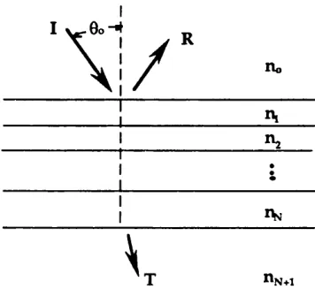
Two parallel m irrors of reflectivities Rf an d separated by a m ed iu m of index nm and thickness L, form a Fabry-Perot cavity. M ultiple reflections betw een the tw o m irrors give rise to interferometric effects that depend upo n th e corresponding optical length Lopt = L n m -co sti/X , w here X is the optical w avelength an d 0 is the angle w ith respect to the normal w ithin the cavity m edium (Fig.2.2.1). The reflectivity R is thus given by [W hitehead et a l, 1989a]
R =
R r (l - Vr^ ) 7 ( ‘ - V i V R 7 ) : + F • sin cp
1 + F • sin2 (p
2.2.1
(p = 2jm mL/X - c o s ^
w here F is the coefficient of finesse given by F = 4^RfRfc j (l --^ R fR ^ )2 , and <{> is the
*
•p* > • pN
U l
0.8 R, =0.95
R, =0.3
0.6
0.4
0.2
0
(m+1) n (m+2)7i (m +3)Jt (m+4)7t m n
(one-way) phase-change through the cavity m edium . D estructive interference at the front surface occurs w hen the m ultiply reflected beam s are in-phase b u t they are in an tip h ase w ith the beam th at is directly reflected at th e front surface (Fig.2.2.1). Therefore, reflection m inim a correspond to transmission m axim a an d occur at equally spaced (2k) intervals of double-trip phase-change through the cavity. The reflectivity
of monochromatic light incident on such a cavity, is m inim um at integral m ultiples of a certain m irror separation, or of angle of incidence, an d , for th e sam e u nd erly in g reason, the spectra of the reflected intensity from a certain fixed cavity exhibit evenly spaced m inim a (transm ission m axim a) (Fig.2.2.1). C o m p lete cancellation of the reflected light at a resonant position can only be attained if the reflectivities of the tw o m irrors are equal (Rf=Rb). Indeed, only u n d e r that condition, are both the phases and the individual am p litu d es such th at th e sum of the com plex a m p litu d e s of the m ultiply reflected beam s is equal in am plitude to that of the directly reflected one.
W ith absorption in the cavity, the effective back reflectivity R^ff is reduced to
The higher the reflectivity of the m irrors the sh arp er the FP resonances and this is described by the cavity finesse
w here now, w ith absorption in the cavity, the coefficient of finesse is given by the
R |ff = R b e ' 2ad
2
.2.2
w here a is the absorption coefficient and d the thickness of the absorbing material. The reflectivity of such a cavity at a resonant wavelength is given by
Rf ( i - R q / R f)2
2.2.3
equivalent F = j , i.e. R^ has been replaced by in the previous expression.
-2.3. THE INTEGRATED FABRY-PEROT MODULATOR
2.3.1. Principles of operation.
FP c a v itie s can b e im p le m e n te d to e n h a n c e th e m a n ife s ta tio n of electro ab sorp tive effects in QWs. The Q W s are then em p lo y ed as a field -d ep en d en t a b s o rb e r (q u a n tu m co n fin ed S tark effect, F ig.2.3.1) th a t d e te rm in e s th e effective re fle c tiv ity of th e b ack m irro r R^ff (eqn.2.2.2). T he refle cted o p tical sig n al of m ono chrom atic light of a w avelength coinciding w ith one of the FP resonances, can be
~ 25000 rHI
0
5 20000
c \ j
5 15000 oi
o U
c i o o o o
o o 5000 C/5
<
0
820 840 860 880
W av elen g th (nm)
14kV /cm 83kV /cm
F ig.2.3.1 The field-induced modulation of the absorption coefficient of quantum wells can be employed to attain a modulation of the reflectivity of
a Fabry-Perot cavity. N orm ally-on operation is obtained at Xj and
norm ally-off at XQ.
controlled in this m a n n er by an electrical signal, thereb y realising voltage-controlled optoelectronic m odulation.
in c o rp o rated in a FP cavity w ith asym m etric (unequal) m irro rs su ch th a t Rf<Rb an d w ith an optical length that leads to a resonance at a (pre-) d esig n ed w aveleng th. The o p e ra tio n is set at th a t reso n an ce, i.e. at a reflectio n m in im u m . F o r su c h an arran g em en t, w ith little or no ab so rp tio n in th e cavity, th e fro n t a n d effective back m irro rs are u n eq u al so that com plete cancellation of th e in terferin g beam s can n o t be accom plished an d therefore the device is reflecting p a rt of the in c id en t intensity. W e w ill refer to this as the on-state (positive logic). If a sufficient a m o u n t of ab so rb in g m e d iu m is introd uced in the cavity so that Rf=R^ff, th e device sw itch es to its off-state the total reflectivity being zero. The q u a n tu m w ell ab so rp tio n serv es to re d u c e the back m irro r an d attain this action. The critical am o u n t of ab so rb e r [otd]c req u ire d to accom plish zero off-state reflectivity is given by
2.3.1
W hen the FP w avelen gth App is set at a w av eleng th lon g er than the zero-bias heavy-hole exciton peak, then at zero bias there is m inim al ab so rp tio n at the resonant
n
5 0 5 9 A AlojGa 0.7AS
. 5 periods: 1' j = 9 5 A GaAs
== 6 0 A Alo3Ga 0 . 7 A S
L =27 A /4
Reflector Stack : 1 2 periods of HL , H H: 6 0 6 A Al 0 iGao gA$
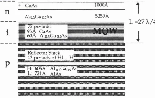
Fig.2.3.2 The epitaxial stru ctu re o f CB145 A F P M that was grow n by M O C V D at the U niversity of Sheffield.
position b ro u g h t abo ut by the ab sorp tion tails of the QW s. T hu s th e d ev ice is at its reflecting state w ith no bias ap p lied . W ith th e a p p ro p ria te bias a p p lie d acro ss the wells, the ab so rp tio n coefficient is increased at the reson ance cau sin g the device to sw itch to its off-state (non-reflecting). The above w o u ld be a so called 'n o rm a lly-o n ' or bias-absorbing device. The o perating w avelen gth w o uld c o rresp o n d typically to Aj in Fig. 2.3.1. By contrast, w ith the resonant w avelength set at the vicinity of the zero-bias exciton peak, the situation is reversed in that the am o un t of ab so rb er th a t is p resen t at
-the resonance drops w ith field. The device is so called 'nor?nally-off or bias-reflecting. Such a device w ould be operating at A*, in Fig.2.3.1. The latter configuration exhibits negative differential resistance (not because of the FP effect b u t certainly enhanced by it) which is a necessary condition for optical bistability [Miller D A B et al., 1989].
It follows from the above that in order to realise an integrated AFPM the structure has to be electrically a p-i-n diode so that bias can be applied across the wells, and optically a FP cavity. The epitaxial stru ctu re of the first AFPM designed by M. W hitehead [1989b] is show n in Fig.2.3.2. The MQWs are incorporated in the intrinsic region of the diode, w hile the FP cavity is form ed betw een the n atu ral front air- sem iconductor interface that is =31 % reflecting and an integrated back m irror that has a reflectivity of =95% in this case. This back reflector is a m ultilayer Bragg stack consisting of alternating quarter w ave layers of high (H) an d low (L) refractive index m aterials, namely AIq jGag^As and AlAs respectively. A brief section on the operation of the Bragg reflector stacks follows later on in this C hapter (section 2.4) and so does information on the growth, device fabrication and experimental testing techniques.
2.3.2. Experimental performance.
Operation as a modulator
Field-dependent reflectivity spectra from a device th at w as fabricated from the structure in Fig.2.3.2, are show n in Fig.2.3.3. The excitonic features m ay be seen clearly in the zero-bias spectra (heavy-hole at =851 nm) w ith the resonant position at a longer w avelength (=862nm). The QCSE-induced shift of the heavy-hole exciton yields a reduction of the resonant reflectivity th at falls to zero a t 9V reverse bias. H igher voltages cause the exciton to shift further from the resonant position and thus lead to an increase of the reflectivity at the resonant (operating) w avelength. The position of the resonance m ay be seen to be voltage dep en d en t. This is caused by th e QW electrorefractive effects that are discussed in the next section. O peration at aro u n d 862nm and at 9V reverse bias exhibits contrast (Ron/ ^0ff^ *n excess ° f 20dB (contrast
characteristic that in the off-state, which is the one th at effectively determ ines the contrast, the cavity is equivalent to one w ith front and back m irrors equal to Rf (R^f = Rf=0.3), resulting in a low finesse of just 2.45 at that state. The w ide resonance does not only lead to a large optical BW b u t it also reflects the general tolerances of the structure, as will be discussed in C hapter 5.
M axim um reflection-change ARmax=48% is obtained at =864nm, i.e. at a longer w avelength than that w here m axim um contrast is achieved. The tw o m axim a do not
FP
0.8
0.6
0.4 - 0V
- 4V - 6V - 8V . 9V - 12V
0.2
hh
830 840 850 860 870 880
W avelength (nm)
Fig.2.3.3 Reflectivity spectra for CB145 AFPM, the epitaxial structure of which is shown in the previous Fig.2.3.2. Data by M. Whitehead.
coincide because w hereas the w avelength of m axim um contrast is determ ined by the position w here the off-state reflectivity is m inim um , the reflection-change is equally governed by both the on- and off-state spectra (subtraction).
The AFPM by far outperform s any oth er vertical m o d u la to r in term s of contrast, reflection-change, and operating voltage. Transm ission an d double-pass reflection m odulators (Chapter 1) are limited mainly by the fact that the im provem ent
of the achieved m odulation dep th w ith increasing num ber of wells levels off d u e to broadening of the absorption spectra w hen the num ber of w ells becom es too large [Stevens, 1989]. Recently, well after the AFPM had been introduced, very good quality MQWs w ith very low background dopings of <1014cm"3 (com pared to the com m on
1 0 15cm '3 ) have been reported [Amano et a l, 1991]. The above m entioned tradeoff is
37-30
03
3
(A
m is
c o U
Insertion Loss 8V
9V 10V 12V
25
20
15
10
5
0
845 850 855 860 865
W avelength (nm)
870 875
Fig.2.3.4 Bias dependent contrast ratio curves and insertion loss obtained from the data in Fig.2.3.3.
2000
-j 1500
|
1000v O o X Oh
500
0
800 820 840 860 880
W avelength (nm)
Fig.2.3.5 Photocurrent spectra for the same device as in Fig.2.3.3. Data by M. Whitehead.
th en b y p assed an d large contrasts (>20dB) m ay be o b tain ed by n on -reso n an t structures. The operating voltages are, how ever, prohibitively high (=30V) for m ost m ajor applications (section 2.5). Symmetric Fabry-Perot m odulators (C hapter 1) that
m ake use of the electrorefractive effects [Simes et al., 1988; Yan et al., 1989b] are highly intolerant structures that m ay yield large reflection-changes b u t at considerably high voltages (25V). Finally, w e ought to m ention that w aveguide m odulators attain large changes at very low voltages, but they are planar structures w ith the advantages and disadvantages this encompasses (Chapter 1). The AFPM com prises thus a small scale breakthrough as far as m odulator characteristics are concerned.
Operation as a detector
In Fig.2.3.5 w e present photocurrent spectra for the same device as above. The spectra are scaled at =750nm to account for the voltage-dependent q uan tu m efficiency. In this way, although the spectra do not correspond to absorptance (A) directly (C hapter 3), the change of photocurrent at each w avelength does correspond to the m odulation of the absorptance. The choice of 750nm is som ew hat arbitrary b u t can be justified as follows. Firstly, this w avelength is shorter than the w avelengths associated w ith both the light-hole exciton and the e l-h h2 forbidden transition bu t at a longer w avelength
than the second order transitions, which has been confirmed by photocurrent spectra of simple p-i-n sam ples of the same well w idth. The im plication therefore is that this part of the absorption spectrum is, to a large extent, not d ep end en t upo n the applied field. Moreover, this was further supported by the fact that u p o n the application of a field the reflectivity spectra at this wavelength did not show a notable change.
The presence of th e Fabry-Perot cavity has a p ro fo u n d effect on the absorptance (A) that is given by
. ( » - * - a d ) P - Rf ) ( ( l - R a )
The features in the photocurrent spectra correspond directly to those in the reflectivity spectra. The m axim um absorption, that occurs at the resonant position at 9V, is estim ated from calculations to be =99%. The AFPM configuration can act, therefore, as a very efficient detector w ithin a wavelength range of =5.5nm. This dual functionality of the AFPM adds another positive point to a long list of advantages over alternative structures. A discussion concerning the m ultiple functionality and large versatility of the AFPM is included in C hapter 9.
l + Rb -e-a d )
2.3.2