R E S E A R C H
Open Access
Multistage quadrature sigma-delta
modulators for reconfigurable multi-band
analog-digital interface in cognitive
radio devices
Jaakko Marttila
*, Markus Allén and Mikko Valkama
Abstract
This article addresses the design, analysis, and parameterization of reconfigurable multi-band noise and signal transfer functions (NTF and STF), realized with multistage quadrature
modulator (Q
M) concept and complex-valued in-phase/quadrature (I/Q) signal processing. Such multi-band scheme was already proposed earlier by the authors at a preliminary level, and is here developed further toward flexible and reconfigurable A/D interface for cognitive radio (CR) receivers enabling efficient parallel reception of multiple noncontiguous frequency slices. Owing to straightforward parameterization, the NTF and the STF of the multistage Q
M can be adapted to input signal conditions based on spectrum-sensing information. It is also shown in the article through closed-form response analysis that the so-called mirror-frequency-rejecting STF design can offer additional operating robustness in challenging scenarios, such as the presence of strong mirror-frequency blocking signals under I/Q imbalance, which is an unavoidable practical problem with quadrature circuits. The mirror-frequency interference stemming from these blockers is analyzed with a novel analytic closed-form I/Q imbalance model for multistage Q
Ms with arbitrary number of stages. Concrete examples are given with three-stage Q
M, which gives valuable degrees of freedom for the transfer function design. High-order frequency asymmetric multi-band noise shaping is, in general, a valuable asset in CR context offering flexible and frequency agile adaptation capability to differing waveforms to be received and detected. As demonstrated by this article, multistage Q
Ms can indeed offer these properties together with robust operation without risking stability of the modulator.
1 Introduction
Nowadays, a growing number of parallel wireless com-munication standards, together with ever-increasing traf-fic amounts, create a widely acknowledged need for novel radio solutions, such as emerging cognitive radio (CR) paradigm [, ]. On the other hand, transceiver implemen-tations, especially in mobile terminals, should be small-sized, power efficient, highly integrable, and cheap [–]. Thus, it would be valuable to avoid implementing paral-lel transceiver units for separate communication modes. However, operating band of this kind of software defined radio (SDR) should be extremely wide (even GHz range),
*Correspondence: jaakko.marttila@tut.fi
Department of Communications Engineering, Tampere University of Technology, P.O. Box 553, Tampere 33101, Finland
and dynamic range of the receiver should be high (several tens of dBs) [–]. In addition, the transceiver should be able to adapt to numerous different transmission schemes and waveforms [–, ]. The SDR concept is considered as a physical layer foundation for CR [], but these de-mands create a big challenge for transceiver design, espe-cially for mobile devices.
Particularly, the analog-to-digital (A/D) interface has been identified as a key performance-limiting bottleneck [, , , , –]. For example, GSM reception demands high dynamic range, and WLAN and LTE bandwidths, in turn, can be up to MHz. Combining this kind of dif-fering radio characteristics set massive demands for the A/D converter (ADC) in the receiver. Traditional Nyquist ADCs (possibly with oversampling) divide the conversion resolution equally on all the frequencies, and thus, if -bit
resolution is needed for one of the signals converted, then similar resolution is used over the whole band even if it would not be necessary []. At the same time, in wideband SDR receiver, the resolution demand might be even higher because of the increased dynamic range due to multiple waveforms with differing power levels entering the ADC.
On the other hand,ADCs have inherent tradeoff
be-tween the sampling frequency and resolution []. With narrowband signals (such as GSM), e.g., -bit resolution can be achieved with -bit quantization because of high oversampling and digital filtering. At the same time, mod-ulator structure can be reconfigured for reception of wide-band waveforms to meet differing requirements set by, for example, WLAN or LTE standards [, , ].
Based on this, one promising solution for the receiver de-sign in this kind of scenario is wideband direct-conversion or low-IF architecture [] with a bandpassADC [, ]. Additional degrees of freedom can be obtained by
introducing quadrature modulator (QM) in the
receiver, allowing efficient frequency asymmetric quanti-zation noise shaping [, ]. Furthermore, a multi-band modulator aimed to CR receivers is preliminary proposed in [] and illustrated with receiver block diagram and principal spectra in Figure . This kind of multi-band de-sign for QM offers frequency agile flexibility and re-configurability based on spectrum-sensing information [] together with capability of receiving multiple paral-lel frequency bands [], which are considered essential when realizing A/D interface for CR solutions []. In prac-tice, multiple noise-shaping notches can be created on in-dependent, noncontiguous signal bands. In addition, the center frequencies of these noise notches can be tuned based on the spectrum-sensing information obtained in the receiver.
Noise-shaping capabilities of a single-stage QM are limited by the order of the modulator []. However, the
order of the overall noise transfer function (NTF) can be increased using cascaded multistage modulator [–]. Therein, the overall noise shaping is of the combined or-der of the stages. In a multistage QM, the noise notches of the stages can be placed independently, thus further in-creasing the flexibility of the ADC [].
Unfortunately, implementing quadrature circuits brings always a challenge of matching the in-phase (I) and quadra-ture (Q) rails, which should ideally have symmetric com-ponent values. Inaccuracies in circuit implementation al-ways shift the designed values, creating imbalance between the rails, known as I/Q imbalance [, ]. This mismatch induces image response of the input signal in addition to the original input, causing mirror-frequency interference (MFI) [, ]. This image response can be modeled math-ematically with altered complex conjugate of the signal
component. In QMs generally, the mismatches
gen-erate conjugate response for both the input signal and the quantization error [, , ], which is a clear differ-ence to mirror-frequency problematics in more traditional receivers. Specifically, feedback branch mismatches have been highlighted as the most important MFI source [, ]. From the noise point of view, placing a NTF notch also on mirror frequency to cancel MFI was initially proposed in [] and discussed further in []. This, however, wastes noise shaping performance from the preferred signal point of view and restricts design freedom, especially in multi-band scenario. In addition, this does not take the mirroring of the input signal into account. In wideband SDR quadra-ture receiver, the MFI stemming from the input of the re-ceiver is a crucial viewpoint because of possible blocking signals. Furthermore, alterations to analog circuitry have been proposed in [, , ] to minimize the interfer-ence. Sharing the components between the branches, how-ever, degrades sampling properties of the modulator [,
]. On the other hand, additional components add to the circuit area and power dissipation of the modulator []. In [], the authors found that mirror-frequency-rejecting signal transfer function (STF) design mitigates the input signal-originating MFI in case of mismatch in the feed-back branch of a first-order QM. In [], this idea is extended to cover multi-band design of [] with a
sim-ple two-stage QM. The feedback I/Q imbalance
ef-fects and related digital calibration in two-stage QM are addressed also in [], where only a frequency-flat STF is considered. In addition, the mirror-frequency-rejecting STF design has a benefit of not demanding additional com-ponents to the original QM structure.
In this article, an analytic closed-form model for QM I/Q imbalance effects is derived covering multistage mod-ulators with arbitrary number of stages, extending the pre-liminary analysis with two first-order stages in []. Herein,
the I/Q imbalance model for second-order QM
pre-sented by the authors in [] is used for each of the stages. Furthermore, design of the transfer functions (STF and NTF) of the stages in such multistage QM is addressed in detail with emphasis on robust operation under I/Q
mis-matches. In [, ], QM STF designs are proposed
for reducing the dynamics of the receiver and to filter ad-jacent channel signals for lowpass and quadrature band-pass modulators, respectively. However, adapting the STF based on spectrum-sensing information is not covered in case of the QM in []. In addition, NTF adaptation to frequency handoffs or multi-band reception is not con-sidered in either [] or []. Herein, frequency agile de-sign of the STF and the NTF of an I/Q mismatched multi-stage QM is discussed taking both the input signal and the quantization noise-oriented MFI into account during multi-band reception.
The push for development of multi-channel ADCs for SDR and CR solutions has been acknowledged, e.g., in []. A multi-channel system with parallel ADCs is one possible solution which, however, sets additional burden for size, cost, and power dissipation of the receiver implementation [, ]. On the other hand, quadrature noise shap-ing makes exploitation of whole quantization precision on the preferred signal bands possible. Three-stage lowpass
modulators have traditionally been used only for ap-plications demanding very high resolution [], but like shown in this article, the QM variant allows noncon-tiguous placement of the NTF zeros, and thus the quan-tization precision can be divided on multiple parallel fre-quency bands. A reconfigurable three-stage converter
us-ing lowpassstages together with a pipeline ADC is
proposed in [] for mobile terminals. In comparison, a three-stage QM discussed in this article offers more efficient noise shaping and additional degrees of freedom for the receiver design. These are essential characteris-tics when heading toward a frequency agile-reconfigurable
ADC for CR receivers. Thus, a multistage QM offers a competent platform for realizing flexible multi-band A/D conversion in CR devices.
The rest of the article is organized as follows. In Sec-tion , basics of quadraturemodulation are reviewed, while Section presents a closed-form model for I/Q im-balance effects in a second-order QM as a single stage of a multistage modulator and proposes a novel extension of the given model for multistage modulators with arbi-trary number of stages. Parameterization and design of the modulator transfer functions in CR receivers in the pres-ence of I/Q mismatches are discussed in Section . The receiver system level targets and QM performance are discussed in Section . Thereafter, Section presents the results of the designs in the previous section with closed-form transfer function analysis and computer simulations. Finally, Section concludes the article.
Short note on terminology and notations: term “order” refers in this article to the order of polynomial(s) in z -domain transfer functions, while term “stage” refers to
in-dividual QM block in a multistage converter where
multiple QM blocks are interconnected. Thez-domain representations of sequences x(k) andx∗(k) are denoted asX[z] andX∗[z∗], respectively, where superscript (·)∗ de-notes complex conjugation.
2 Basics of quadrature
modulation
Quadrature variant of the modulator was originally
presented in []. The concept is based on the modula-tor structure similar to the one used in real lowpass and bandpass modulators, but employing complex-valued in-put and outin-put signals together with complex loop filters (integrators). This complex I/Q signal processing gives ad-ditional degree of freedom to response design, allowing for frequency-asymmetric STF and NTF. For analysis pur-poses, a linear model of the modulator is typically used. In other words, this means that quantization error is as-sumed to be additive and having no correlation with the input signal. Although not being exactly true, this allows analytic derivation of the transfer functions and has thus been applied widely, e.g., in [, ]. Now, the output of a single-stage QM, depicted in Figure , is defined as
Videal[z] =STF[z]U[z] +NTF[z]E[z], () where STF[z] and NTF[z] are generally complex-valued functions, andU[z] and E[z] denotez-transforms of the input signal and quantization noise, respectively.
Figure 2 Discrete-time linearized model of aPth-order QM with complex-valued signals and coefficients.
NTF of thePth-order QM is given by
NTF[z] =
–Pp=Rppi=z–Mi
()
and, on the other hand, the corresponding STF is
STF[z] =A+
P
p=Bp
p
i=z–Mi
–Pp=Rppi=z–Mi
, ()
where /(z–Mi) terms are the transfer functions of the
complex loop filters (integrators). Both transfer functions have common denominator and thus common poles. It can also be seen that in addition to the loop filters, only the feedback coefficients Rp (feeding the output to the loop
filters) affect the noise shaping. Thus, input coefficientsA
(feeding the input to the quantizer) andBp(feeding the
in-put to the loop filters) can be used to tune the STF zeros independent of the NTF.
The NTF zeros are usually placed on the preferred sig-nal band(s) to create the noise-shaping effect. At the same time, the STF zeros can be used to attenuate out-of-band frequencies and thus include some of the receiver selectiv-ity in the QM. The transfer function design for CR is
discussed in more detail in Section . In the following sub-sections, multi-band and multistage principles will be pre-sented. These are important concepts, considering refigurability in the A/D interface and frequency agile con-version with high-enough resolution in CR devices.
2.1 Multi-band quadratureADC for CR
With QM of higher than first order, it is possible to place multiple NTF zeros on the conversion band []. Tra-ditional way of exploiting this property has been making the noise-shaping notch wider, thus improving the resolu-tion of the interesting informaresolu-tion signal over wider band-widths []. However, in CR-based systems, it is desirable to be able to receive more than one detached frequency bands - and signals - in parallel []. The multi-band scheme offers transmission robustness, e.g., in case of appearance of a primary user when the CR user has to vacant that fre-quency band []. In that case, the transmissions can be con-tinued on the other band(s) in use. In addition, if the CR traffic is divided on multiple bands, then lower power lev-els can be used, and thus the interference generated for pri-mary users is decreased [].
Multi-band noise shaping without restriction to fre-quency symmetry is able to respond to this need with noncontiguous NTF notches. This reception scheme is il-lustrated graphically in Figure . The possible number of
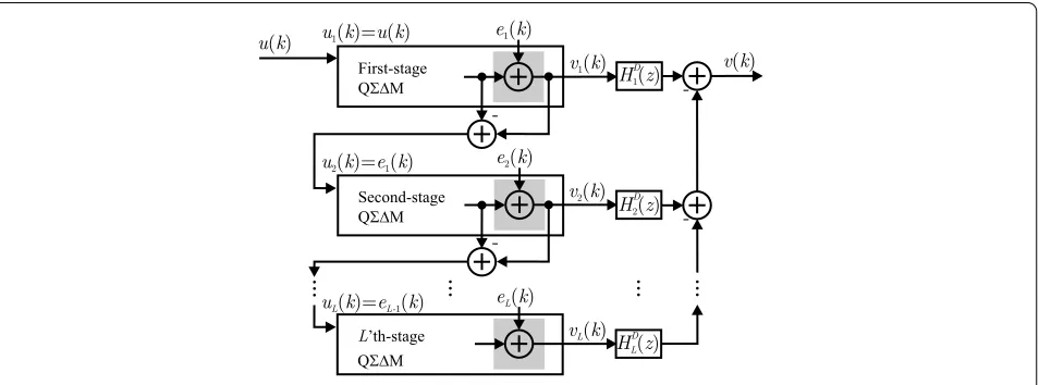
Figure 4 Multistage QM with arbitrary-order noise shaping in all the individual stages.FiltersHD
1[z] toHDL[z] are implemented digitally.
these notches is defined by the overall order of the mod-ulator. With multistage QM this is the combined or-der of all the stages. In addition, the frequencies of the notches can be tuned straightforwardly, e.g., in case of fre-quency handoff. This tunability of the transfer functions allows also for adaptation to differing waveforms, center frequencies and bandwidths to be received. The resolution and bandwidth demands of the waveforms at hand can be
taken into account and the response of the QM can
be optimized for the scenario of the moment based on the spectrum-sensing information. Further details on design and parameterization of multi-band transfer functions are given in Section .
3 Multistage quadrature
ADC
Multistagemodulators have been introduced to
im-prove resolution, e.g., in case of wideband information sig-nal, when attainable oversampling is limited. This prin-ciple was first proposed with lowpass modulator [], but has thereafter been extended to quadrature bandpass modulator [, ]. The block diagram ofL-stage quadra-ture ADC is given in Figure , where all the stages are of arbitrary order. The inputsul(k) of theLindividual
stages (≤l≤L,l∈Z) are defined in the following man-ner. The input of the first-stage (l= ) is the overall input of the whole structure, i.e.,u(k) =u(k), and for the lat-ter stages, the (ideal) input is the quantization error of the previous stage; thus,ul(k) =el–(k) when ≤l≤L.
The main goal in multistage QM is to digitize quan-tization error of the previous stage with the next stage and thereafter subtract it from the output of that previ-ous stage. Owing to the noise shaping in the stages, the digitized error estimate must be filtered in the same way, in order to achieve effective cancelation. Similarly, the out-put of the first stage must be filtered with digital equivalent
of the second-stage STF (e.g., to match the delays). These filters are depicted in Figure withHD
[z] toHLD[z]. Now,
assuming ideal implementation, the final output becomes
Videal[z] =
L
l=
(–)l+HlD[z]Vlideal[z], ()
where
Vlideal[z] =STFideall [z]Ul[z] +NTFideall [z]El[z],
≤l≤L,l∈Z, ()
and
HlD[z] =H D [z]
L–
l= NTFideall [z]
L
l=STFideall [z]
, ≤l≤L,l∈Z, ()
to match the analog transfer functions and the digital fil-ters. It is usually chosen thatHD[z] =STF[z], thus giving
HD[z] =NTF[z] and HD[z] =NTF[z]NTF[z]/STF[z], etc. With these selections, the quantization errors of the earlier stages are canceled (assuming ideal circuitry), and the overall output of theL-stage QM becomes (L≥)
Videal[z] =STFideal [z]STFD[z]U[z] +
L
l=NTFideall [z]
L
l=STFideall [z]
EL[z]
=STFidealTOT[z]U[z] +NTFidealTOT[z]EL[z],
()
Figure 5 Discrete-time-linearized model of thelth second-order QM stage in a multistage QM with complex-valued signals and coefficients.
the third and the latter stages, which operate in the denom-inator of the noise-shaping term. However, the leakage of the quantization noise of the earlier stages might be lim-iting achievable resolution in practice because of nonideal matching of the digital filters []. One way to combat this phenomenon is to use adaptive filters [, ].
3.1 I/Q imbalance in multistage QMs
In this section, a closed-form transfer function analysis is carried out for a general multistage QM taking also the possible coefficient mismatches in complex I/Q signal pro-cessing into account. For mathematical tractability and no-tational convenience, second-order QM stages are as-sumed as individual building blocks (individual stages) in Figure , and the purpose is to derive a complete closed-form transfer function model for the overall multistage converter. Such analysis is missing from the existing state-of-the-art literature. For notational simplicity, the modu-lator coefficients are denoted in the following analysis as shown in the block diagram of Figure . With this struc-ture, the ideal NTF for thelth stage is given by
NTFl[z] =
– (M(l)+N(l))z–+ (M(l)N(l))z–
/ – (M(l)+N(l)+R(l))z–
+ (M(l)N(l)+N(l)R(l)–S(l))z–.
()
At the same time, the ideal STF for thelth stage is defined as
STFl[z] =
A(l)+ (B(l)–N(l)A(l)–M(l)A(l))z–
+ (C(l)–N(l)B(l)+M(l)N(l)A(l))z–
/ – (M(l)+N(l)+R(l))z–
+ (M(l)N(l)+N(l)R(l)–S(l))z–.
()
The transfer functions of () and () are valid when I and Q rails of the QM are matched perfectly. With this per-fect matching, () and () give the outputs for single-stage and multistage modulators, respectively.
3.2 I/Q imbalance effects on individual QM stage
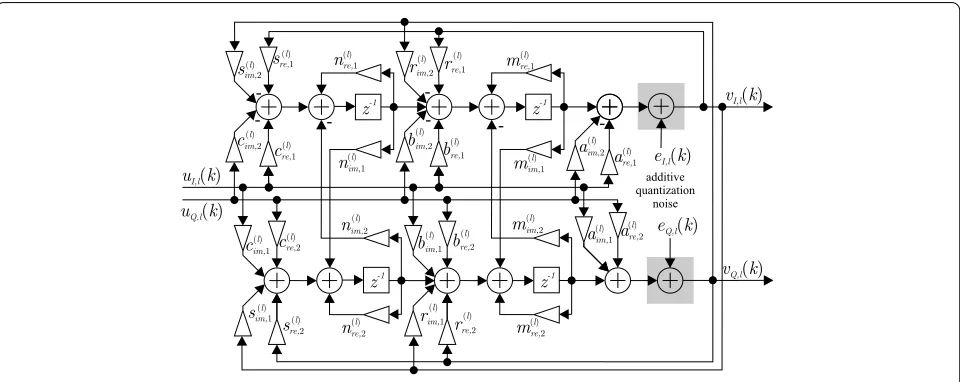
Quadrature signal processing is, in practice, implemented with parallel real signals and coefficients. In Figure , this is demonstrated in case of a single second-order QM stage (parallel real I and Q signal rails) and taking pos-sible mismatches in the coefficients into account. Devia-tion between coefficient values of the rails, which should ideally be the same, results in MFI. This interference can be presented mathematically with conjugate response of the signal and the noise components. Thus, image signal transfer function (ISTF) and image noise transfer function (INTF) are introduced, in addition to the traditional STF and NTF, to describe the output under I/Q imbalance. In the following, an analytic model is presented, first for in-dividual stages of a multistage QM, and then for I/Q
mismatched multistage QM, having arbitrary number
of stages, as a whole. Such analysis has not been presented in the literature earlier.
The I/Q imbalance analysis for a single stage is based on the block diagram given in Figure . In this figure, real and imaginary parts of the coefficients of Figure are marked with subscripts re and im, whereas nonideal implementa-tion values of the signal rails are separated with subscripts and . The independent coefficients of the stages are de-noted with superscriptl. Thus, to obtain the complex out-putsVl[z] =VI,l[z] +jVQ,l[z] of the stages (l∈ {,L}), the
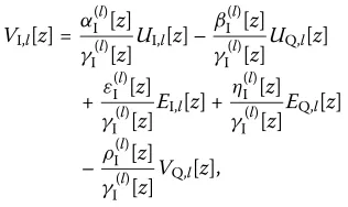
I branch outputs can be first shown to be
VI,l[z] =
αI(l)[z]
γI(l)[z]UI,l[z] –
βI(l)[z]
γI(l)[z]UQ,l[z] +ε
(l) I [z]
γI(l)[z]EI,l[z] +
ηI(l)[z]
γI(l)[z]EQ,l[z] –ρ
(l) I [z]
γI(l)[z]VQ,l[z],
()
Figure 6 Implementation structure of thelth second-order QM stage in a multistage QM with parallel real signals and coefficients taking possible mismatches into account.
following manner:
αI(l)[z] =are,(l) + [b(re,l) –m(re,l) a(re,l) –n(re,l) a(re,l)
+n(im,l) a(im,l) +m(im,l) a(im,l) ]z– + [c(re,l) –n(re,l) bre,(l) +n(re,l) m(re,l) a(re,l)
–n(re,l) m(im,l) aim,(l) +n(im,l) b(im,l)
–n(im,l) mim,(l) a(re,l) –nim,(l) m(re,l) a(im,l) ]z–, ()
βI(l)[z] =aim,(l) + [b(im,l) –n(re,l) a(im,l) –n(im,l) a(re,l)
–m(re,l) a(im,l) –m(im,l) a(re,l) ]z– + [c(im,l) –n(re,l) bim,(l) +n(re,l) m(re,l) a(im,l)
+n(re,l) m(im,l) are,(l) –n(im,l) b(re,l)
–n(im,l) mim,(l) a(im,l) +nim,(l) m(re,l) a(re,l) ]z–, ()
εI(l)[z] = – [nre,(l) +m(re,l) ]z–
+ [n(re,l) m(re,l) –nim,(l) m(im,l) ]z–, ()
ηI(l)[z] = [nim,(l) +m(im,l) ]z–
– [n(re,l) m(im,l) +nim,(l) m(re,l) ]z–, ()
ρ(Il)[z] = [n(im,l) +rim,(l) +m(im,l) ]z– – [s(im,l) –n(re,l) rim,(l) –n(im,l) r(re,l)
–n(re,l) m(im,l) –nim,(l) m(re,l) ]z–,
()
γI(l)[z] = – [n(re,l) +r(re,l) +m(re,l) ]z– + [s(re,l) –n(re,l) rre,(l) +n(im,l) rim,(l)
–n(re,l) m(re,l) +nim,(l) m(im,l) ]z–.
()
This follows directly from a step-by-step signal analysis of the implementation structure in Figure . Similarly, the real-valued Q branch outputs are given by
VQ,l[z] =
βQ(l)[z]
γQ(l)[z]UI,l[z] +
αQ(l)[z]
γQ(l)[z]UQ,l[z]
+ ε
(l) Q[z]
γQ(l)[z]EQ,l[z] –
η(Ql)[z]
γQ(l)[z]EI,l[z]
+ρ
(l) Q[z]
γQ(l)[z]VI,l[z],
()
where
αQ(l)[z] =are,(l) + [b(re,l) +n(im,l) a(im,l) –n(re,l) a(re,l)
+m(im,l) a(im,l) –m(re,l) a(re,l) ]z– + [c(re,l) –n
(l) re,b
(l) re,–n
(l) im,m
(l) im,a
(l) re,
+n(im,l) b(im,l) –nim,(l) m(re,l) a(im,l)
–n(re,l) mim,(l) a(im,l) +nre,(l) m(re,l) a(re,l) ]z–,
()
βQ[z] =a(im,l) + [b (l) im,–n
(l) im,a
(l) re,–n
(l) re,a
(l) im,
–m(im,l) a(re,l) –m(re,l) a(im,l) ]z– + [c(im,l) –n(re,l) bim,(l) –n(im,l) m(im,l) a(im,l)
–n(im,l) b(re,l) +nim,(l) m(re,l) a(re,l)
+n(re,l) mim,(l) a(re,l) +nre,(l) m(re,l) a(im,l) ]z–,
()
εQ(l)[z] = – [nre,(l) +m(re,l) ]z–
ηQ(l)[z] = [nim,(l) +m(im,l) ]z–
In this way, the complex-valued output and the exact be-havior of each transfer function can be solved analytically in different I/Q mismatch scenarios. As a result, the com-plex output of an individual stage with nonideal matching of the I and Q branches becomes
Vl[z] =VI,l[z] +jVQ,l[z]
=STFl[z]Ul[z] + ISTFl[z]Ul∗[z∗]
+NTFl[z]El[z] + INTFl[z]El∗[z∗],
()
where superscript asterisk (*) denotes complex conjuga-tion, and the transfer functions are, based on () and () (omitting [z] from the modulator coefficient variables of ()-() and ()-() for notational convenience), given by
In Section ., the above analysis for the individual stages
l∈ {,L}is combined to complete the closed-form overall
model for the multistage QM.
Based on (), the converter output consists of not only the (filtered) input signal and quantization noise but also their complex conjugates, which, in frequency domain, corresponds to spectral mirroring or imaging. Thus, based on (), the so-called image rejection ratios (IRRs) of the
lth stage are
where actual frequency-domain responses are attained with the substitution z← ejπfTS to the earlier transfer functions, where f is the frequency measured in Hertz andTSis the sampling time. These IRR quantities describe the relation of the direct input signal and noise energy to the respective mismatch-induced MFI at the output sig-nal. As an example,IRR()STF(ejπfTS) = dB means that the power of the mismatch-induced (mirrored) conjugate input signal is dB lower than the direct input signal at the frequencyf. Similarly,IRR()NTF(ejπfTS) = dB
indi-cates that the nonconjugated quantization error level is dB above the mirror image of the quantization error at the frequencyf. Notice also that, in general, both IRRs are frequency-dependent functions.
3.3 Combined I/Q imbalance effects of the stages in
multistage QM
For multistage QM, as illustrated in Figure , the final output signal is defined as a difference of digitally filtered output signals of the stages []. Furthermore, like shortly discussed already, the first-stage inputU[z] =U[z] while forl> ,Ul[z] =El–[z]. The output of the first stage, given by () withl= , is filtered with digital filterHD
[z] (usually matched to the STF of the second stage) and the output of the second stage, similarly given by () withl= , is filtered withHD
ReplacingVl[z] in () with () forl∈ {,L}gives now
an expression for the overall output as
V[z] =
where the transfer functions are as defined in ()-(). Again, the digital filters are assumed matched to the analog transfer functions according to (). As a concrete example, () can be evaluated for a three-stage (L= ) QM, giv-structurally to the ideal output given in (). However, the responses of STFTOT[z] andNTFTOT,[z] can be al-tered when compared to STFidealTOT[z] and NTFidealTOT[z] be-cause of possible common-mode errors in the modu-lator coefficients []. Consequently, the six additional terms in () are considered as mismatch-induced in-terference, which includes the leakage of the first- and second-stage noises and the corresponding MFI (con-jugate) components. It should also be noticed that the first-stage quantization error termsSTFD[z]NTF[z]E[z] andNTFD[z]STF[z]E[z] do not reduce to zero because of noncommutativity of the complex transfer functions under I/Q imbalance []. On the other hand, second-stage quantization error vanishes ifNTFD[z]NTF[z] and (NTFD[z]NTFD[z]/STFD[z])STF[z] are equal. This means thatNTFD
[z] andSTFD[z] should be equal to their analog counterparts, which can realized with, e.g., adaptive dig-ital filters [, ]. The matching can also be made more robust by designing the third stage to have unity signal re-sponse (STF[z] = ).
Now, based on (), it is clear that filtered versions of the original and conjugate components of the input, the first-stage, the second-first-stage, and the third-stage quantization errors all contribute to the final output. In order to inspect the overall IRR of the complete multistage structure, the transfer functions of the original signals (the input and the errors) and their conjugate counterparts should be com-pared. Based on (), this gives the following formulas for the three-stage case considered herein:
nonidealities. This can be expressed with interference re-jection ratio. In case of a three-stage QM, following from (), the signal component (interference-free output) is defined as
σ(k) =STFTOT(k)∗u(k) +NTFTOT,(k)∗e(k), () where impulse responses of the STF and third-stage NTF are convolving the overall input and third-stage quantiza-tion error, respectively. At the same time, the total interfer-ence component (total additional interferinterfer-ence caused by the nonidealities) is defined as
where time-domain signal components are again con-volved by respective transfer function impulseresponses. It should be noted that, in case of ideal three-stage QM, () reduces to zero. Now, interference rejection ratio at any given useful signal band is given by the integrals of spectral densitiesGσ(ejπfTS) andGτ(ejπfTS) of the above
where integration is done over the preferred signal band, defined asC,={fC,–W/, . . . ,fC,+W/}(whereWis the bandwidth of the signal). If there are two parallel sig-nals (two-band scenario), the interference rejection ratio of the second signal is calculated in similar manner:
=
An example of interference rejection ratio analysis in receiver-dimensioning context is given in Section . In ad-dition, the roles of the separate signal components are fur-ther illustrated with numerical results in Section .
4 Q
M transfer function parametrization and design for CR under I/Q imbalance
In CR-type wideband receiver, signal dynamics can be tens of (even -) dBs [, ]. With such signal composition, controlling linearity and image rejection of the receiver
components is essential [, , ]. In this section, we
con-centrate on QM transfer function design under I/Q
imbalance, having minimization of input signal oriented MFI as the goal.
4.1 Transfer function parametrization for reconfigurable CR receivers
The NTF and STF of a QM can be designed by
plac-ing transfer function zeros and poles, parameterized and
tuned (allowing reconfigurability) by the QM
coeffi-cients, inside the unit circle []. In the following, the de-sign process is described for a second-order QM as a single-stage converter or an individual stagelof a multi-stage converter. This is then extended to multimulti-stage con-verters in Section ..
Based on the numerator of (), the NTF zeros of the second-order QM are defined by the loop-filter feed-back coefficients, i.e.,
ϕNTF,(l) =M(l)=λNTF,(l) ejπfNTF,(l) TS, ()
andfpole,(l) , are the frequencies of the poles. The coefficients
M(l)andN(l)are already fixed according to (), leavingR(l) andS(l)free to tune the pole placement. The poles can, e.g., be placed on the frequency bands of the preferred signals to elevate the STF response and thus give gain for the pre-ferred signals. However, the pole placement elevates also the STF response, and thus this kind of design is always a tradeoff between the noise-shaping and STF selectivity efficiencies.
On the other hand, the loop-filter coefficients (M(l)and
N(l)) have also their effects on the STF zeros, which, how-ever, can be further tuned with the input coefficients (A(l),
B(l), andC(l)) of the modulator. This is illustrated in case of second-order QM, based on (), by the expressions
ϕSTF,(l) = (/A(l))(A(l)M(l)+A(l)N(l)–B(l)) + (/A(l))(B(l)+A(l)M(l)+A(l)N(l) + A(l)B(l)M(l)– A(l)B(l)N(l)
– A(l)M(l)N(l)– A(l)C(l))/ =λ(STF,l) ejπfSTF,(l) TS,
()
ϕSTF,(l) = (/A(l))(A(l)M(l)+A(l)N(l)–B(l)) – (/A(l))(B(l)+A(l)M(l)+A(l)N(l) + A(l)B(l)M(l)– A(l)B(l)N(l)
– A(l)M(l)N(l)– A(l)C(l))/ =λ(STF,l) ejπfSTF,(l) TS,
()
where λ(STF,l) =|ϕSTF,|(l) and λ(STF,l) =|ϕ(STF,|l) . Thus, ()-() clearly show that A(l), B(l), andC(l) allow indepen-dent placement of the STF zeros. In proportion to the NTF zero analysis above, fSTF(l), and f
(l)
STF, are the frequencies of the two STF notches. The proposed way to design the STF includes setting fSTF,(l) and fSTF,(l) to be the mirror fre-quencies of the preferred information signals (based on the spectrum-sensing information) to attenuate possible blockers on those critical frequency bands. More generally, these frequencies, and thus the STF zero locations, can be tuned to give preferred frequency-selective response for the STF. On the other hand, if frequency-flat STF design is preferred, then the zeros can be set to the origin by setting
λ(STF,l) andλ(STF,l) to zero.
Usually, the first step in the QM NTF and STF
de-sign is to obtain the placements of the zeros and the poles as already discussed above. Thereafter, the modulator co-efficient values realizing those zeros and poles should be found out. In the following, this procedure is explained for a second-order QM as thelth stage of a multistage QM. Practically, the goal is to find values for the input coefficients (A(l),B(l), andC(l)), the loop-filter coefficients
(M(l) andN(l)) and the feedback coefficients (R(l)andS(l)) that realize the STF zeros (ϕSTF,(l) andϕSTF,(l) ), the NTF ze-ros (ϕ(NTF,l) andϕNTF,(l) ), and the common poles (ψcommon,(l)
andψcommon,(l) ) fixed above based on the transfer function characteristics.
The numerator of the NTF, the numerator of the STF, and the denominator of both transfer functions are used to solve the coefficient values. To begin with, the loop-filter feedback coefficientsM(l) andN(l), the numerator of the NTF can be expressed with the modulator coefficients of the respective stage, as in (), or with the help of the re-spective zerosϕNTF,(l) andϕNTF,(l) . Setting these expressions equal, i.e.,
– (M(l)+N(l))z–+ (M(l)N(l))z–
= – (ϕ(NTF,l) +ϕNTF,(l) )z–+ (ϕNTF,(l) ϕNTF,(l) )z–, () allows for solving the coefficient values of the lth stage based on the zeros by setting the terms with similar delays equal. Thus,
M(l)+N(l)=ϕNTF,(l) +ϕ(NTF,l) , ()
M(l)N(l)=ϕNTF,(l) ϕNTF,(l) , () giving
M(l)=ϕ(l)
NTF,, ()
N(l)=ϕNTF,(l) . ()
This result confirms that the NTF zeros are set by the complex-valued feedback gains of the loop integrators.
The input coefficientsA(l),B(l), andC(l) of thelth stage can be solved in similar manner, based on the STF numer-ator given in (). Next, the numernumer-ator of () is set equal to the STF numerator presented with the respective zeros
ϕ(STF,l) andϕ(STF,l) , i.e.,
A(l)+ (B(l)–N(l)A(l)–M(l)A(l))z– + (C(l)–N(l)B(l)+M(l)N(l)A(l))z–
= – (ϕSTF,(l) +ϕ(STFl) .)z–+ (ϕSTF,(l) ϕSTF,(l) )z–. ()
Now,A(l),B(l), andC(l)can be solved setting the separate delay components equal. This gives
A(l)= , ()
B(l)=N(l)A(l)+M(l)A(l)– (ϕSTF,(l) +ϕSTF,(l) ), ()
pronouncing that these coefficient can be used to tune the STF response. However, the NTF zeros should also be taken indirectly into account because they define the val-ues ofM(l)andN(l), as found out in ()-().
At this point, only the feedback coefficientsR(l)andS(l)
of thelth stage remain unknown. Those can be solved us-ing the common denominator of the NTF and the STF in () and (). Again, the denominator of () and () is set equal to the denominator presented with the common poles of the transfer functionsψcommon,(l) andψcommon,(l) . In
Again, setting the separate delay components equal gives solutions for the feedback coefficients:
R(l)= –M(l)–N(l)+ψcommon,(l) +ψcommon,(l) , ()
S(l)=M(l)N(l)+N(l)R(l)–ψcommon,(l) ψcommon,(l) . () Thus, the feedback gains are affected by the NTF zeros (again viaM(l)andN(l)) but finally defined by the poles of both the transfer functions.
Based on this parametrization, tuning the modulator response in frequency agile way is straightforward. The spectrum-sensing information is used to extract the in-formation about the frequency bands preferred to be re-ceived, and NTF zeros are placed on these frequencies (fNTF,(l) andfNTF,(l) in second-order case) with unity mag-nitude (λ(NTF,l) = and λ(NTF,l) = in second-order case). In addition, the most harmful blockers can be identified based on the spectrum sensing. Thus, the STF zeros can be set on the unit circle (λ(STF,l) = andλ(STF,l) = in second-order case) on the frequencies of those blocker signals (fSTF,(l) andfSTF,(l) in second-order case). The poles can be used to tune both the transfer functions, being common though. Usually, the frequencies that are attenuated in the NTF design are supposed not to be attenuated in the STF and vice versa. This sets an optimization problem for the pole placement. Pole placement in the origin is of course a neutral choice. The authors have chosen poles on the preferred signal center frequencies, i.e.,fpole,(l) =fNTF,(l) and
fpole,(l) =fNTF,(l) , to highlight STF selectivity with gain on the preferred signal bands. The magnitudes of the poles are chosen to beλ(pole,l) = . andλ(pole,l) = ., thus pulling the poles half way off the unit circle to maintain efficient quan-tization noise shaping. A summary table of the overall
de-sign flow will be presented, after discussing the dede-sign as-pects under I/Q imbalance, at the end of the following sub-chapter.
4.2 Multistage QM transfer function design under
I/Q imbalance
In QMs, the modulator feedback branch mismatches
have been considered most crucial [, , ]. Exactly this problem can be fought against with mirror-frequency-rejecting STF design in a single-stage QM [] or in the first stage of multistage QM []. The signal fed to the feedback branch of the modulator is the same as in the out-put, so the STF and NTF effects are seen therein in full ex-tent. Considering this together with potential blocking sig-nal energy on the mirror band, mirror-frequency-rejecting STF design is a recommended choice for feedback branch-mismatched QMs based on the analysis in [, ].
The main difference in this design compared to the one proposed in [] is deeper notching of the mirror-band(s) to attenuate possible input blocker(s) as effec-tively as possible. This is attained by setting the STF ze-ros on the unit-circle at the mirror-frequencies of the preferred information signals, meaning in second-order
case thatϕ()STF,=λ()STF,ejπfSTF,() TS=e–jπfNTF,() TSandϕ() placed on the preferred signal center frequencies, as de-scribed above, to elevate the STF response, i.e.,ψcommon,() =
.ejπfNTF,() TS andψ()
common,= .e
jπfNTF,() TS (withλ() pole,= . andλ()pole,= .).
In multistage QMs, the latter stages process only the quantization error of the preceding stage, and thus the STFs of these stages do not contribute to the overall input– output STF. This can be seen also in (), where the overall STF is a product of the first-stage STF and the following digitalHD
all theLstages. Thus, the order of the first stage is lim-iting the capabilities to implement the mirror-frequency-rejecting STF design, e.g., in multi-band reception. The benefits of mirror-frequency-rejecting STF design will be demonstrated graphically and numerically in Section us-ing the earlier closed-form response analysis results and computer simulations.
Considering the NTF design of the stages under I/Q
imbalance (a three-stage QM used as an example),
the role of the digital second-stage filterHD[z] =NTFD[z] is emphasized. In ideal case, the overall noise present at the output should be the noise of the last stage shaped by the product of all the stage NTFs. Thus, notching of each of the preferred signal frequency bands could be done in any of the stages having similar overall effect. However, under I/Q imbalance, quantization errors of the stages have also image response components, e.g.,
NTFD
[z]ISTF[z] for E∗[z] and –NTFD[z]INTF[z] for
E∗[z] (see ()). Naturally, these terms are preferred to be minimized on all the interesting frequency bands. Thus, it is proposed to place the NTF zeros of the first stage at the center frequencies of the preferred information sig-nals, i.e., ϕNTF() ,=ejπfC,TS and ϕ()
NTF, =ejπfC,TS, where
fC, and fC, are the center frequencies of the two sig-nals to be received. With the latter stage(s), the noise notches can widened by placing the respective NTF zeros around the ones of the first-stage NTF. This means that,
e.g., in three-stage scenarios, the second-stage zeros are
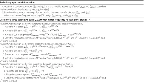
ϕ()NTF,=ejπ(fC,±foffset,)TS andϕ() widths) for optimal zero placements []. The signs in the exponent terms are opposite for the second- and the third-stage zeros. The ideal model would allow also for such NTF design that the noise shaping of the interesting frequency bands would be done separately in different stages, mean-ing, e.g., that the first-stage NTF would notch the frequen-cies of certain signal and the second-stage NTF the fre-quencies of the other one. However, this kind of approach would allow the underlying I/Q imbalance-induced im-age components to leak more heavily on the latter signal band. The above-mentioned NTF design is proposed to avoid this scenario. This overall design flow, starting with spectrum-sensing information in terms of preferred sig-nal center frequencies and blocker center frequencies, is illustrated as a whole in Table .
5 Receiver system level considerations
In this section, system level parameters are considered to define realistic target values for the needed interfer-ence rejection ratio introduced in Section . The proposed QM performance is illustrated in a realistic multi-band
Table 1 Overall design flow of a three-stage two-band QM.
Preliminary spectrum information
1. Obtain the center frequencies (fC,1andfC,2) and the suitable frequency offsets (foffset,1andfoffset,2) based on the bandwidths of the desired signals, e.g., from [36]
2. Based on the spectrum sensing information, find the most harmful blockers (fint,1andfint,2)
•In case of mirror-frequency rejecting STF designfint,1= –fC,1andfint,2= –fC,2
Design of a three-stage two-band QM with mirror-frequency rejecting first-stage STF
Transfer function design for the first-stage (two-band NTF and mirror-frequency rejecting STF) 1. Place the NTF zeros:ϕ(1)NTF,1=ej2πfC,1TS,ϕ(1)
Transfer function design for the second-stage (two-band NTF and frequency-flat STF) 5. Place the NTF zeros:ϕ(2)NTF,1=ej2π(fC,1+foffset,1)TS,ϕ(2)
reception scheme, assuming the sampling frequencyfS= MHz.
The detection of a -QAM waveform on intermedi-ate frequency fC,-QAM= . MHz with bandwidth of
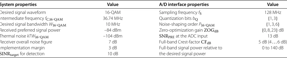
W-QAM = MHz is considered as a practical exam-ple. The received preferred signal power is assumed to be – dBm (sensitivity level), remaining dB above the thermal noise floor at – dBm. Taking typical receiver overall noise figure of dB into account, this gives signal-to-noise ratio (SNR) of dB at the input of the ADC (SNRPRE= dB). Thus, with digital signal-to-interference and noise ratio (SINR) target of say dB (SINRtarget = dB) for detection, implementation margin of dB is al-lowed.
Different combinations of QM parameters are
con-sidered to highlight the flexibility of the structure, namely first-, third-, and sixth-order, noise shaping (P-QAM = {, , }) is applied for the preferred signal band in - and -bit quantization schemes (bQ={, }). The noise-shaping order P-QAM describes the combined noise-shaping
ef-fects of all the QM stages on that frequency band
according to the discussion in Sections and , assum-ing an ideal QM. The related zero-optimization gains for each noise-shaping order (ZOGdB={, , }) are ob-tained from [] and represent the SNR gain of the optimal zero placements compared to the case where all the zeros are on the center frequency of the preferred signal.
The Crest factors in the range of to dB were found in simulations with realistic power levels for a number of out-of-band signals in addition to the preferred one, de-pending on the exact power distribution (the simulation setup will be further discussed in Section ). Thus, Crest factor of CFdB= dB is assumed in the following analysis for the sake of simplicity. The full-band signal power to the preferred signal power ratio is assumed to range from dB (only the preferred signal) up to + dB. Such a high max-imum value is chosen to illustrate also the performance of the sixth-order efficient noise shaping. The properties de-fined above are summarized in Table .
Based on the given parameters, signal-to-quantization
noise ratio (SQNR) of the QM, yet without
imple-mentation nonidealities, can be solved in different sce-narios by varying the amount of quantization bits and
noise-shaping order. The SQNR equations derived for real lowpass modulators [] of corresponding order can be adopted to use also in quadrature bandpass case because the noise-shaping efficiency is maintained with only asym-metric shift of the NTF notch center frequency. Thus, the inband SQNR for a single-frequency channel (assuming an ideal QM), taking also receiver out-of-band signal con-tent into account, is defined as
SQNR = .bQ+ . – CFdB
where, in addition to the values given in Table ,Sfull-band is the power of the whole ADC input signal, andS-QAM is the power of the preferred -QAM waveform. Increas-ing full-band signal power compared to the preferred sig-nal power decreases the SQNR because with large values of this ratio, the out-of-band signal content dominates the dynamics of the overall signal. In this kind of scenario, the weak preferred signal is effectively scaled down at the ADC input. Now, the total SNR after the A/D conversion (SNRTOT) is the ratio of signal powerS-QAMto the com-bined inband thermal noise powerNPREand inband quan-tization noise power NQ (NTOT =NPRE +NQ). Further-more, this ratio can be defined with SNRPRE and SQNR, giving
In addition, SINRtargetset for the detection defines also the maximum level of additional inband interference
com-Table 2 A summary of receiver system level and A/D interface properties used in the interference rejection example.
System properties Value A/D interface properties Value
Desired signal waveform 16-QAM Sampling frequencyfS 128 MHz
Intermediate frequencyfC,-QAM 36.74 MHz Quantization bitsbQ {1, 3}
Desired signal bandwidthW-QAM 10 MHz Noise-shaping orderP-QAM {1, 3, 6}
Received preferred signal power –84 dBm Zero-optimization gainZOGdB {0, 8, 23}dB
Thermal noisekTW-QAM –104 dBm SNRPREat the ADC input 13 dB
Receiver overall noise figure 7 dB Full-band Crest-factorCFdB 5 dB (4. . .6 dB)
Implementation margin 3 dB Full-band signal power relative to
the desired signal power
0 to 140 dB
ponents other than thermal and quantization noises, such
as MFI and noise leakage, generated by the
modula-tor nonidealities, discussed in Section . In that section, interference rejection ratiowas defined to measure the amount of this interference relative to the ideal modula-tor output inband power. Now, the maximum tolerable amount of additional inband interferenceIMAX, compared to the preferred signal, the inband thermal noise and the inband quantization noise powers (S-QAM+NTOT), de-fines the needed interference rejection ratio demanded to fulfill the set SINRtarget. Thus, interference rejection ratio is given by
demand= log
S-QAM+NTOT
IMAX
= log +
–SNRTOT/
–SINRtarget/– –SNRTOT/
,
SNRTOT> SINRtarget.
()
If SNRTOTis below SINRtarget, achieving the set SINR is obviously not possible and a logarithm of a negative num-ber results in a complex-valueddemand(hence the condi-tion SNRTOT> SINRtarget).
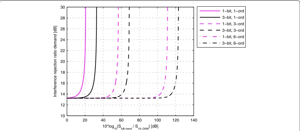
This interference rejection demand is plotted in Figure as a function of the full-band signal power compared to the preferred inband signal power. The increasing power ratio on thex-axis limits the performance of the ADC be-cause of the decreasing SQNR according to (). Subse-quently, from () it is clear that, if SNRTOT approaches SINRtarget, then the denominator goes to zero and thus
demandgoes to infinity, indicating that no additional in-terference is allowed. The flooring at approximately dB
happens because, this is, together with the thermal noise SNR of dB, the minimum level of interference rejection ratio with any SQNR to achieve the SINR target of dB. The six QM scenarios with - or -bit quantization and differing noise-shaping orders on the preferred signal band defined above are illustrated in Figure as examples. The most straightforward case for multi-band reception of parallel signals with the bandwidths in megahertz-range is third-order noise shaping with - or -bit quantization, al-lowing two signal bands to be converted efficiently. These results are plotted with dashed lines and show tolerance of the full-band power to signal power ratios up to the range of to dB, depending on the quantization scheme. The first- and sixth-order noise shapings are applicable for the conversion of narrow- and wideband signals, respectively. However, the results given in Figure are applicable only with given exemplary set of parameters (see Table ), such as -MHz bandwidth. The derived interference rejection ratio demands are compared to the simulated achievable figures of the proposed QM design in Section .
6 Results and illustrations
In this section, the models derived in Section and the design principles in Section are used to analytically cal-culate and illustrate the transfer functions for a three-stage QM under I/Q imbalance (Section .). Finally,
the QM behavior under I/Q imbalance is simulated
to illustrate the interference rejection performance of the modulator (Section .) for which the target values were derived in Section .
In general, multi-band IF reception [] of two par-allel information signals around center frequencies of
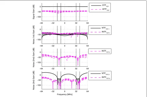
Figure 8 Three-stage QM STF and ISTF (top) together with NTF and INTF for first-, second-, and third-stage quantization noises.Five independent random realizations in real gain values of feedback branches of both stages andflat STF design in all the stages. Multi-band reception of two information signals with center frequencies of 36.74 and –15.74 MHz is assumed. These bands are marked withgray solid linesin the plots.
fC,= . MHz andfC,= –. MHz is assumed with sampling frequency of fS= MHz (giving TS = /fS = . ns). These bands, with bandwidth of W=W = MHz, are marked in Figures and with vertical gray lines. The frequency offsets from the center frequencies for the outermost NTF zeros arefoffset,=foffset,=
√ /∗ MHz = . MHz, setting those zeros close to the inter-esting band edges.
The transfer functions of the stages are designed in the following manner, based on the above-described sce-nario and the discussion on design flow in Section . Third-order noise shaping is designed for both the sig-nal bands, allowed by the overall NTF order of six. The first-stage NTF has unit-circle zeros on the center frequen-cies of the two signals, thus ϕNTF,() =ejπfC,TS =ejπ. andϕNTF,() =ejπfC,TS=e–jπ.. The second-stage zeros,
ϕNTF,() = ejπ(fC,+foffset,)TS = ejπ. and ϕ() NTF, =
ejπ(fC,+foffset,)TS =e–jπ., are used to widen the noise-shaping notches toward higher frequencies. The lower frequencies of the interesting bands are notched by the third-stage NTF zeros ϕNTF,() =ejπ(fC,–foffset,)TS =ejπ.
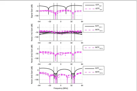
andϕNTF,() =ejπ(fC,–foffset,)TS =e–jπ.. With frequency-flat STF designs, the STF zeros and the common poles are placed in the origin. In the mirror-frequency-rejecting STF design considered for the first stage, the zeros of the first-stage STF are placed on respective mirror frequen-cies, givingϕSTF,() =e–jπ. andϕ()
STF,=ejπ.. At the same time, the common poles of the first-stage trans-fer functions are placed on the signal center frequencies, i.e., ψcommon,() = .ejπ. and ψ()
common,= .e–jπ., to highlight the STF selectivity and to maintain efficient noise shaping. Based on this design, the modulator co-efficients are solved separately for each second-order stage as discussed above (see ()-()). The digital filters
HD
[z],HD[z], andHD[z] are assumed to be matched per-fectly to the analog transfer functions as described above.
6.1 Transfer function analysis
Figure 9 Three-stage QM STF and ISTF (top) together with NTF and INTF for first-, second-, and third-stage quantization noises.Five independent random realizations in real gain values of feedback branches of both stages andmirror-frequency-rejecting STF design in first stage. Multi-band reception of two information signals with center frequencies of 36.74 and –15.74 MHz is assumed. These bands are marked withgray solid linesin the plots.
realization of the real part of the mismatched first-stage modulator feedback gain becomes rre,() = ( +
r()re,)r
() re,
whererre,() is the implementation value andr()re the ideal value. First, the transfer functions are analyzed and illus-trated in a case of second-order three-stage QM with flat STF design in all the stages. The effects of I/Q im-balance are demonstrated by introducing mismatch to the feedback branches (coefficientsR(l)andS(l)in Figure ) of the stages. Five independent realizations of each transfer function, calculated with described mismatches, are plot-ted to demonstrate effects of inaccuracies on modulator response. The resulting transfer functions are shown in Figure . The overall ISTF response averages at – dB level, varying between – and – dB over the frequency. While the overall STF has dB response, this results in averagely dB image rejection for the input signal. The three latter plots in Figure present the responses for the first-, second-, and third-stage quantization errors, respec-tively. The noise responses show that third-stage error is well shaped showing all six notches of the stages. Also the third-stage conjugate-noise (MFI stemming from the
quantization error) is well attenuated, e.g., due to the dig-ital filterHD
[z] =NTFD[z]NTFD[z]/STFD[z], which gives nice attenuation on the interesting frequency bands. First-stage error is leaking to the output due to noncommutativ-ity of mismatched complex transfer functions. However, attenuation on the preferred signal bands is still on aver-age at the level of – dB for the first-staver-age quantization error and – dB for the conjugate component. However, when discussing noise responses, it should be remembered that large power variations as in the input blocker scenario are improbable. The second-stage nonconjugate noise is effectively canceled, but the conjugate version is visible at the output. This second-stage mirror-noise is, however, shaped by the NTF of the first stage, as mentioned in Sec-tion , and thus nicely attenuated on the preferred signal bands.