Leakage Power Optimization of Linear
Feedback Shift Register (LFSR)
Rebecca Angela Fernandes
1, Niju Rajan
2P.G. Student, Department of E&C Engineering, N.M.A.M Institute of Technology, Karnataka, India1
Assistant Professor, Department of E&C Engineering, N.M.A.M Institute of Technology, Karnataka, India2
ABSTRACT: The major concern in modern VLSI circuits is to design the circuit for low power testing. In the circuit leakage power increases with increase in scaling of the devices. Out of the available solutions, power-gating has proved to be very efficient in reducing the stand-by leakage currents in the idle mode. Sleep transistor is the basic element which is used in power gating technique for shutting down the power for a portion of the design. The basic idea of power gating is to separate the 𝑉𝐷𝐷 or GND power supply from the standard cells of the specific design hierarchy. Appropriate sized PMOS or NMOS transistors are used as sleep transistor. A method to reduce the power consumption of the popular Linear Feedback Shift Register is presented. A traditional 8-bit Linear Feedback Shift Register (LFSR) without power gating technique is implemented and the leakage power report is then compared with LFSR designed using different power gating techniques..
KEYWORDS: Power Gating, Leakage power dissipation, Fine Grain Power Gating (FGPG), Coarse Grain Power Gating (CGPG).
I. INTRODUCTION
Most electronic circuits and system design are confronted with the problem of delivering high performance with a limited consumption of electronic power. High performance is required by the increasing complex applications (e.g., multimedia) that are running even on portable devices. Low power consumption is required to achieve acceptable autonomy in battery-powered systems as well as to reduce the environmental impact (e.g., heat dissipation, cooling-induced noise). In other words, achieving highly energy-efficient computation is a major challenge in electronic design.
Static and dynamic power dissipations are the two major issues for the power consumption during test. Leakage current contributes to static power dissipation and it is very small in VLSI circuits. Dynamic power dissipation is large and it is due to the switching activity within the test patterns. Reduction of the dynamic power in the circuit will reduce the test power in VLSI circuits.
Leakage power is a major concern in CMOS technologies and numerous design techniques have been introduced to reduce stand-by leakage in digital circuits. Reducing the static power dissipation has become extremely important during periods of inactivity to develop design techniques. Without trading-off performance the power reduction must be achieved which makes it harder to reduce leakage during operation at runtime. In sleep or standby mode to reduce the leakage power, several techniques are used. A well-known technique is Power gating technique where a sleep transistor is added between virtual ground & actual ground rail. In the sleep mode to cut-off the leakage path, the device is turned-off. This technique provides a substantial reduction in leakage at a minimal impact on performance.
II. LITERATURE SURVEY
the power gating technique. A comparison of the outputs by designing a conventional Adder and an Adder using Sleep Transistor is obtained. The results have shown that power gating using sleep transistor had reduced the leakage power. Jiang et al., [7], explained the benefits and cost of power gating technique. They have considered a standard chip and a power-gated chip both implementing the same functionality. In the standard chip, all logic circuits are connected to 𝑉𝐷𝐷 through a hierarchical power mesh. The entire chip is fully powered at all times. In the power-gated chip, they have used local power meshes for all macros, and sleep transistors are used to connect the local mesh to the global mesh. Their results show that power-gating has proved to be very efficient in reducing the stand-by leakage currents in the idle mode. Verma et al., [8], explained the important and vital parameters such as sizing of sleep transistor, mode transition energy, reduction of noise, area, delay and noise margin that need to be considered while using the power gating technique. Abba et al., [9], presented the different techniques of power gating. The techniques are as follows: 1) Fine Grain Power Gating and 2) Coarse Grain Power Gating.
III.LINEARFEEDBACKSHIFTREGISTER
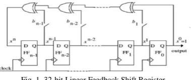
The LFSR is a shift register with is designed using an array of D flip-flops and XOR gates. The XOR gates are used to perform linear functions. There are two types of LFSR’s-external feedback LFSR’s and internal feedback LFSR’s. The maximum-length of an LFSR sequence is 2n-1.Fig .1 shows a traditional 32-bit LFSR with a maximum length of the
sequence 232-1[13] [14].
Fig. 1. 32-bit Linear Feedback Shift Register
IV.POWER GATING
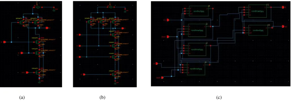
Fine Grain Power Gating (FGPG): Process of adding a sleep transistor to every cell is called Fine grain power gating as shown in Fig.2 (a). Sleep transistor is added to every cell that is to be turned off imposes a large area penalty and individually gating the power of every cluster of cells creates timing issues introduced by inter-cluster voltage variation, these are very difficult to resolve.
(a) (b).
Fig. 2. Types of power gating (a) Fine Grain Power Gating (b) Coarse Grain Power Gating
V. IMPLEMENTATION
D flip-flop and Linear Feedback Shift Register (LFSR) circuits are designed using Cadence Virtuoso tool with 90nm CMOS technology. The transient analysis is done by launching ADEL for verification of schematic results. The power report is obtained for D flip-flop and 8-bit Linear Feedback Shift Register (LFSR) with and without using power gating technique.
(a) (b) (c)
Fig. 3. Schematic (a) 2-input NAND gate with FGPG (b) 3-input NAND gate with FGPG (c) D flip-flop with FGPG
(a) (b) (c)
Fig. 4. Schematic (a) 2-input NAND gate with CGPG (b) 3-input NAND gate with CGPG (c) D flip-flop with CGPG
Fig .4(a) shows the schematic of 2-input NAND gate and Fig .4(b) shows the 3-input NAND gate, where only one sleep transistor needs to be inserted between all the NAND circuits used to design the D flip-flop. These circuits are used to design the D flip-flop with Coarse Grain Power Gating (CGPG).Fig.13 shows the schematic of D flip-flop using Coarse Grain Power Gating (CGPG), where one sleep transistor (N-MOS) is inserted between the virtual and actual ground rail of all the NAND gates.
(a) (b)
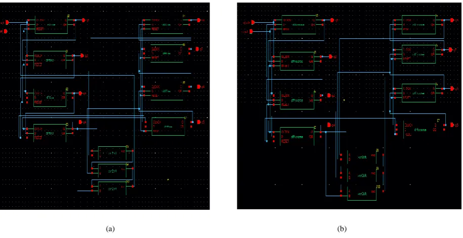
Fig. 5. Schematic (a) 8-bit LFSR with FGPG (b) 8-bit LFSR with CGPG
The 8-bit Linear Feedback Shift Register (LFSR) sequences through (28-1) states, where 8 is the total number of shift
linear functions. The maximum-length of an LFSR sequence is 28-1. The 8-bit LFSR is designed for the polynomial 𝑥8 + 𝑥6 + 𝑥5 + 𝑥4 + 1 as shown in Fig .5(a) and (b).
VI.POWER ANALYSIS
The Leakage power dissipation is calculated using Cadence tool Calculator
Table I Power Analysis of D flip-flop
Table I shows the leakage power of a normal D flip-flop and also power gated D flip-flop’s with Fine Grain Power Gating (FGPG) and Coarse Grain Power Gating (CGPG) techniques. There is 9.52% leakage power reduction in D flip-flop implemented using Fine Grain Power Gating (FGPG) technique and 29.60% leakage power reduction in D flip-flop implemented using Coarse Grain Power Gating (CGPG) technique compared to the normal D flip-flop.
Table II Power Analysis of 8-bit LFSR
8-bit LFSR Leakage Power Dissipation 8-bit LFSR without power
gating
347.8 nW
8-bit LFSR with Fine Grain Power Gating
262.4 nW
8-bit LFSR with Coarse Grain Power Gating
131.9nW
Table II shows the leakage power of a normal 8-bit LFSR and also power gated 8bit LFSR implemented using D flip-flop with Fine Grain Power Gating (FGPG) and Coarse Grain Power Gating (CGPG) techniques. There is 24.55% leakage power reduction in 8-bit LFSR implemented using Fine Grain Power Gating (FGPG) technique and 62.07% leakage power reduction in 4-bit LFSR implemented using Coarse Grain Power Gating (CGPG) technique compared to the normal 8-bit LFSR.
VII. CONCLUSION
The 8-bit Linear Feedback Shift Register (LFSR) has been designed for the polynomial 𝑥8 + 𝑥6 + 𝑥5 + 𝑥4 + 1. The D-flip flop and LFSR were designed using Cadence Virtuoso tool. The leakage power of normal D D-flip-flop and 8-bit LFSR
D flip-flop Leakage Power Dissipation
D flip-flop without power
gating 30.77 nW
D flip-flop with Fine Grain
Power Gating 27.84 nW
D flip-flop with Coarse Grain
has been compared with the power gated D flip-flop and 8-bit LFSR, it is observed that there is leakage power reduction in the power gated circuits when compared to the normal circuits.
REFERENCES
[1] Zorian Y., “A Distributed BIST Control Scheme for Complex VLSI Devices”, IEEE CS Press, Los Alamitos, Calif., 1993, pp 4-9. [2] Girard P. L., Guiller C., Landrault, Pravossoudovitch S., Wunderlich H. J.,2001, “A modified Clock Scheme for a Low Power BIST Test Pattern
Generator”, pp 306-311.
[3] Nourani M., Tehranipoor M., Ahmed N, “Low-Transition Test Pattern Generation for BIST-Based Applications”, IEEE Transactions on Computers,New York, Volume 3,Issue 15,2008, pp 303-315.
[4] Abromovici M., Breuer M.A., Friedman,“Digital Systems Testing and Testable Design”, NJ: IEEE Press,1990,pp. 182-196, pp. 457-468, and pp 477-481.
[5] C. Chrisjin Gnana Suji, S. Maragatharaj and R.Hemima, “Performance Analysis of Power Gating designs in Low Power VLSI Circuits”, International Conference on Signal Processing, Communication, Computing and Networking Technologies,2011.
[6] R. Vara PrasadaRao,N. Anjaneya Varaprasad,G. Sudhakar Babu and C. Murali Mohan,“Power Optimisation of Linear Feedback Shift Register (LFSR) for low power BIST implemented in HDL”, International Journal of Modern Engineering Research, Volume 3,Issue. 3, May-June.2013, pp 1523-1528.
[7] Hailin Jiang, Malgorzata Marek-Sadowska, and Sani R. Nassif,“Benefits and cost of Power Gating”, International Conference on Computer Design,2005.
[8] Preeti Verma,Arti Noor,Ajay K.Sharma and Sampath Kumar V,“Power Gating and its Repercussions-A Review”, International Conference on Power Electronics, Intelligent Control and Energy Systems,2016.
[9] Akhila Abba and K Amarender, “Improved Power Gating Technique for Leakage Power Reduction”, International Journal Of Engineering And Science, Volume 4, Issue 10, October 2014, pp 06-10.
[10] Chuan-Yu Wang and Kaushik Roy, “Maximum Power Estimation for CMOS Circuits Using Deterministic and Statistical Approaches”, IEEE Transactions on Very Large Scale Integration Systems, Volume 6, Issue 1, MARCH 1998.
[11] J. Lee and N. A. Touba,"LFSR-Reseeding Scheme Achieving Low Power Dissipation During Test", IEEE Transactions on Computer-Aided Design of Integrated Circuits and Systems, Volume 26, Issue 2, Feb. 2007,pp. 396-401.
[12] Yasmeen Khan, “Power Optimization of Linear Feedback Shift Register Using Clock Gating”,International Journal of Engineering Research and Development,Volume 7, Issue 1, May 2013, pp. 109-115.
[13] Saraswathi T., Ragini. K. and Ganapathy Reddy Ch,“A Review on Power optimization of Linear Feedback Shift Register (LFSR) for Low Power Built In Self Test (BIST)”, Electronics Computer Technology (ICECT), 3rd International Conference, pp. 172-176, 2011.
[14] Balwinder Singh, Arun Khosla and Sukhleen Bindra, “Power Optimization of Linear Feedback Shift Register (LFSR) for Low Power BIST”, Advance Computing Conference, IEEE International, pp. 311-314, 2009.
[15] Chi-Yi Yeh, Hung-Ming Chen, Li-Da Huang, Wei-Ting Wei, Chao-Hung Lu and Chien-Nan Liu, “Using Power Gating Techniques in Area-Array SoC Floorplan Design”, SOC Conference, IEEE International, pp. 233-236, 2007.
[16] Madhushree K. and Niju Rajan, “Dynamic Power Optimization of LFSR Using Clock Gating”, International Conference on Innovations in Information, Embedded and Communication Systems (ICIIECS), vol. 5, pp. 429-432, 2017.
[17] Madhushree K. and Niju Rajan, “Dynamic Power Optimization Using Look-Ahead Clock Gating Technique”, IEEE International Conference On Recent Trends In Electronics Information Communication Technology, pp. 258-262, 2017.
[18] Amit Kumar Panda, Praveena Rajput and Bhawna Shukla, “ FPGA Implementation of 8, 16 and 32 bit LFSR with Maximum Length Feedback Polynomial Using vhdl”, International Conference System and Network Technology, 2012.
[19] Kawal .K, Saluja, “Linaer Feedback Shift Register Theory and Application”, Department of Electronics and Communication Engineering, University of Wisconsin, Madison, Oct 1988.