ABSTRACT
NA, JEONG-SEOK. Nanoscale Assembly for Molecular Electronics and In Situ
Characterization during Atomic Layer Deposition. (Under the direction of Dr. Gregory N. Parsons.)
The work in this dissertation consists of a two-part study concerning molecular-based electronics and atomic layer deposition (ALD). As conventional “top-down” silicon-based technology approaches its expected physical and technical limits, researchers have paid considerable attention to “bottom-up” approaches including molecular-based electronics that self assembles molecular components and ALD techniques that deposit thin films with atomic layer control.
after trapping over short-term and long-term time scales. The real-time monitoring of conductance through dimer structures during trapping offers immediate detection of a specific fault which is ascribed to a loss of active molecules and fusing of the nanoparticles in the junction occurring mostly at a high applied voltage (≥3 VAC). After successful trapping, the sample exposure to air reveals a small rapid decrease in current, followed by a slower exponential increase, and eventual current saturation.
This work also reports on the dependence of electron transport on molecular length (2 to 4.7 nm) and structure (linear-type in dimers and Y-type in trimers). The extracted electronic decay constant of ~0.12 Å-1 and effective contact resistance of ~4 MΩ indicate a strong electronic coupling between the chain ends, facilitating electron transport over long distances. A three terminal molecular transistor is also demonstrated with trimers trapped across nanogap electrodes. The source-drain current is modulated within a factor of 2 with a gate bias voltage of −2 to +2 V. A subthreshold slope of ~110 mV/decade is obtained.
Finally, we report on both fundamental understanding and application of atomic layer deposition. First, in situ analysis tools such as quartz crystal microbalance and electrical
Nanoscale Assembly for Molecular Electronics and In Situ Characterization
during Atomic Layer Deposition
by
Jeong-Seok Na
A dissertation submitted to the Graduate Faculty of North Carolina State University
in partial fulfillment of the requirements for the degree of
Doctor of Philosophy
Chemical Engineering
Raleigh, North Carolina 2009
APPROVED BY:
_______________________________ ______________________________ Dr. Gregory N. Parsons Dr. Christopher B. Gorman
Chair of Advisory Committee
DEDICATION
This dissertation is dedicated to my wife, Sung Kyung Song,
my parents, Il Song Na and Im Soon Song,
and my parents-in-law,Eun Geun Song and Sun Hee Won
BIOGRAPHY
Jeong-Seok Na was born in the small town of Soonchang in South Korea in 1973.
Then he and his family moved to Kwangju where he was raised until 1992. During that
period, he graduated from Korea High School in 1992 and was accepted into the Chemical
Engineering at Hanyang University, Seoul. After receiving his Bachelor Degree in 1999, he
continued studying at Pohang University of Science and Technology (POSTECH) to earn his
Master’s Degree in which his research focused on the metalorganic chemical vapor
deposition and characterization of high dielectrics ZrO2 and TiO2 thin films using novel
precursors for application in an alternative of SiO2 gate dielectrics of a transistor. After
graduation in 2001, he joined the central research and development center, Samsung
Electro-Mechanics Company in the city of Suwon, South Korea. After working in industry as a
senior researcher for three and a half years, he decided to pursue an advanced doctoral degree
in Chemical Engineering at North Carolina State University, Raleigh in the fall of 2004.
Under the excellent guidance of Dr. Gregory Parsons, he focused on the fundamental
research related to the nanoscale assembly and charge transport measurements in
ACKNOWLEDGMENTS
This dissertation would not have been possible without direct or indirect contributions
from a number of people. First, I would like to thank my advisor, Dr. Gregory Parsons, for
his intellectual insights and generous advices on matters both professional and personal. He
has strengthened the ability of my own independent and rational thinking during PhD
research as well as realizing my ideas. I would also like to thank Dr. Christopher Gorman, Dr.
Jan Genzer, and Dr. Orlin Velev for serving on my dissertation committee.
I would like to express my gratitude to Jennifer Ayres and Dr. Kusum Chandra,
co-workers, for synthesizing nanoparticle assembly samples for a molecular electronics project.
I am indebted to Chuck Mooney, Roberto Garcia and Fred Stevie for SEM, TEM and
SIMS measurements, respectively, at Analytical Instrumentation Facility (AIF) and also Joan
O’Sullivan, David Vellenga and Marcio Cerullo for helping me prepare samples using metal
evaporation, stepper, ICP-RIE, respectively, at Nanofabrication Facility (NNF).
I would also like to thank the office staffs in the Chemical and Biomolecular
Engineering department for their support, and especially the graduate secretary, Sandra
Bailey, for taking care of official documents and Kit Yeung for providing solutions in fixing
and moving deposition equipments.
I have had a great time with my colleagues in the Parsons Research Group. The
cleanroom fabrication process and diverse characterization skills for a molecular electronics
project that I learned from Dr. Changwoong Chu are gratefully acknowledged. I also want to
acknowledge Dr. Kiejin Park for helping me understand the ALD equipment and process.
also want to acknowledge Dr. Giovanna Scarel for FT-IR measurements and passionate
discussion on my research, Qing Peng for in situ QCM measurements and sharing creative
ideas on various experiments as a classmate and a group member, and Dr. Jesse Jur for
revising my dissertation. Also, I like to acknowledge the other group members for helping in
the completion of my dissertation work - Joe Spagnola, Dr. David Terry, Dr. Jason Kelly, Dr.
Kevin Hyde, Michael Stewart, Bo Gong, Dohan Kim, Kyoungmi Lee, and Christina Devine.
I wish you all a great success in your future.
I also want to express my sincere appreciation to the people in my life that made these
five years the best years of my life: All my “school” friends and alumni - Yongjae Choi, Dr.
Youngkuk Jhon and Dr. Suktai Chang for their sincere assistance and friendship and Dr.
Jaehoon Kim and Dr. Changshin Park for their help with my initial settle down in the US; All
my “soul” friends - Jaehwan Lim, Yonghee Cho, Dr. Bongkyu Chang and Cheolwan Park for
their heartfelt concern and prayer for my family; All of my “church” members that I have
interacted with, especially the Bible study members - Dr. Sangjung Oh, Dr. Mookyung
Cheon, Dr. Wooseob Shim, and Sungjin Cho, and also Elder Mansung Yim for spending a
time in teaching the Bible and frankly sharing his life and faith with me as a spiritual mentor.
I also like to express my endless love and gratitude to my family, especially my wife,
Sung Kyung Song for her sacrifice, love and prayer for five years without which I could not
have finished my dissertation, and also my parents and parents-in-law for their unconditional
affection and prayer.
Finally, I would like to thank God for his grace, guidance, and being with me all the
TABLE OF CONTENTS
Lists of Tables ………. ix
Lists of Figures ……… x
1. Objective and introduction ……… 1
1.1 Objective of this work ……….. 2
1.2 Background of molecular-based electronics ……… 3
1.2.1 Charge transport properties of organic molecules ………... 3
1.2.2 Fabrication and characterization of metal-molecule-metal junctions …….. 7
1.2.3 Assembly of particles between the electrodes ………. 16
1.3 Background of atomic layer deposition ……… 21
1.4 Experimental approach ………. 25
1.4.1 Physical and chemical characterization ………... 25
1.4.2 Electrical characterization ……… 29
1.4.3 In situ characterization during atomic layer deposition ………... 31
1.5 Outline of this dissertation ……… 34
1.6 References ………. 38
2. Key Advances in molecular electronics developed in this work ………. 46
3. Key Advances in atomic layer deposition developed in this work ………. 51
4. Conduction mechanisms and stability of single molecule(s) nanoparticle/molecule/ nanoparticle junctions ………. 59
4.1 Abstract ……….. 60
4.2 Introduction ……… 61
4.3 Experimental methods ……… 62
4.4 Results and discussion ……… 63
4.5 Conclusions ……… 81
4.6 References ……….. 83
5. Real-time conductivity analysis through single-molecule electrical junctions ... 87
5.1 Abstract ……….. 88
5.2 Introduction ……… 89
5.3 Experimental methods ……… 90
5.4 Results and discussion ……… 95
5.5 Conclusions ……… 105
5.6 References ……….. 107
6. Dependence of molecular length and structure on electron transport through single molecule nanoparticle/molecule/nanoparticle junctions ……… 110
6.1 Abstract ……….. 111
6.3 Experimental methods ……… 114
6.4 Results and discussion ………... 116
6.5 Conclusions ……… 130
6.6 References ……….. 131
7. Toward three-terminal molecular devices using nanoparticle/Y-type molecule/ nanoparticle trimeric structure ……….. 135
7.1 Abstract ……….. 136
7.2 Introduction ……… 137
7.3 Experimental methods ……….... 138
7.4 Results and discussion ……… 140
7.5 Conclusions ……… 148
7.6 References ……….. 150
8. Nano-encapsulation and stabilization of single–molecule/particle electronic Nano-assemblies using low-temperature atomic layer deposition ………... 152
8.1 Abstract ……….. 153
8.2 Introduction ……… 155
8.3 Experimental methods ……… 157
8.4 Results and discussion ……… 160
8.5 Conclusions ……… 178
8.6 References ……….. 180
9. Role of doping sequence and surface reactions during atomic layer deposition of Al-doped ZnO ………... 183
9.1 Abstract ……….. 184
9.2 Introduction ……… 185
9.3 Experimental methods ……… 186
9.4 Results and discussion ……… 191
9.5 Conclusions ……… 208
9.6 References ……….. 210
10. Correlation in charge transfer and mass uptake revealed by real-time conductance and quartz crystal microbalance analysis in low temperature atomic layer deposition of zinc oxide and aluminum-doped zinc oxide ………… 213
10.1 Abstract ……… 214
10.2 Introduction ……….. 215
10.3 Experimental methods ……….. 216
10.4 Results and discussion ……….. 218
10.5 Conclusions ……….. 233
using sequential hydrothermal crystal synthesis and thin film atomic layer
deposition ……….. 238
11.1 Abstract ……….. 239
11.2 Introduction ……… 240
11.3 Experimental methods ……… 243
11.4 Results and discussion ……… 245
11.5 Conclusions ……… 265
LIST OF TABLES
Table 1.1 Electronic transports between saturated alkane chains and π-bonded
molecules ………. 5
Table 1.2 Possible conduction mechanisms ………. 6
Table 1.3 Dielectric constants of various materials ………. 20
Table 1.4 Vibrational mode assignments for the molecular junctions investigated … 31
Table 4.1 Experimental trapping results of a OPE-linked gold nanoparticles dimer ... 70
Table 6.1 The measured values of β for conjugated molecules connected to metal
electrodes with different experimental systems ……….. 113
Table 6.2 Gap distance (G) between two nanoparticles as a function of the radius of
a nanoparticle (R) and the estimated molecular length (L) ……… 119
Table 6.3 The statistical distribution of synthesized dimers and trimers with different molecular length ………. 120
Table 6.4 Comparison of linear resistance and conductance (at 1V) between dimers
LIST OF FIGURES
Figure 1.1 The molecules described in the text. (a) Wires; (b) hybrid molecular
electronic (HME) switches; (c) HME rectifiers; (d) storage; and (e) two molecules showing promise for mono-molecular electronics ………. 4
Figure 1.2 Schematic showing the crossed-wire tunnel junction ……….. 8
Figure 1.3 Schematics of a nanometer-scale device with a nanometer-scale pore
etched through a suspended silicon nitride membrane showing a Au-
SAM-Au junction formed in the pore area ……….. 9
Figure 1.4 Scanning electron microscope image of the lithographically fabricated
break junction ……….. 11
Figure 1.5 Field-emission scanning electron micrographs of a representative gold
nanowire (a) before and (b) after the breaking procedure. The nanowire consists of thin (~10 nm) and thick (~90 nm) gold regions ……… 13
Figure 1.6 Scheme of the conducting probe atomic force microscopy experiment.
Voltages are applied to the tip; the substrate is kept at ground.
Measurements are performed in air ………. 14
Figure 1.7 The principle of optical trapping of a single particle by a focused laser
beam ………. 16
Figure 1.8 (a) Illustration showing the fabrication of hemispherically metallized silica microspheres and their magnetic controlled assembly onto SAM-
functionalized electrodes. (b) SEM image showing such a microsphere
junction ……… 18
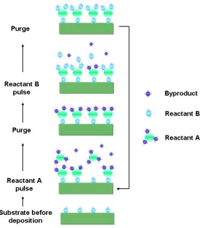
Figure 1.9 Schematic illustration of one ALD reaction cycle ……….. 22
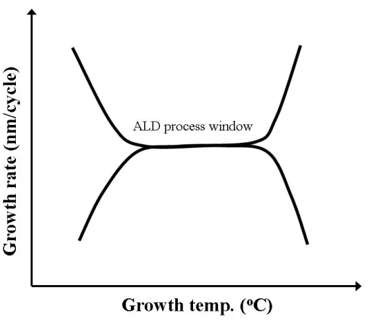
Figure 1.10 Schematic behavior of growth rate versus growth temperature in ALD
process ………. 23
Figure 1.11 Schematic representations of the current-voltage, the conductance-voltage,
Figure 1.12 (a) Schematic view of in situ QCM measurement attached to an ALD reactor. (b) Schematic view of in situ QCM with Ar purge on the back
side of quartz crystal ………... 33
Figure 1.13 Schematic view of in situ conductance measurement attached to a
reactor ……….. 34
Figure 4.1 (a) The molecular structure of the oligomeric phenylene ethynylene
molecule (OPE) bridged by gold nanoparticles. (b) TEM image of a OPE-linked nanoparticle dimer consisting of gold nanoparticles with a
diameter of ~40 nm ……….. 64
Figure 4.2 Schematic structure of a nanogap electrode fabricated by angled metal
evaporation onto a micro-gap electrode. Pd (30 nm) was evaporated onto
the Au(90 nm)Ti(10 nm)/SiO2(150 nm)/p-type silicon substrate with a tilt
angle of ~40o. Metals were evaporated at a rate of ~0.5 Å/s in a chamber
pressure of ~1.0E-7 Torr. The nanogap structure of ~70 nm was formed between the electrodes ………. 65
Figure 4.3 Simulation results of electrical field distribution using FEMLAB. (a)
Electric field contour in the electrodes with a nanogap of ~70 nm. The white solid arrow directs the increasing electrical field gradient. (b) Electrical field distribution containing a single OPE-linked gold nanoparticle dimer between the nanogap electrodes. The electric potential was assumed 2 V ……….. 68
Figure 4.4 (a) Atomic force microscopy (AFM) image of the OPE-linked gold
nanoparticle dimer trapped between the electrodes with ~70 nm nanogap. (b) Schematic drawing corresponding to the line profile of (a), where the red solid line is the real line profile across a trapped dimer ………. 71
Figure 4.5 Current versus voltage characteristics for seven different devices with a single OPE-linked gold nanoparticle dimer trapped between the nanogap electrodes at 2 VAC, 1 MHz, and 60 sec. All the data points are the average values of five measurements on each individual structure ……….. 72
Figure 4.6 Current versus voltage characteristics when applied up to 2 V for the OPE-
Figure 4.7 Temporal current versus voltage fluctuations with 100 cycles of measurements under vacuum of ~5×10⁻⁴ Torr for about 7 hours. Only 40 out of 100 current versus voltage traces are shown here ………. 76
Figure 4.8 Temperature dependent charge transport characteristics through a single
OPE-linked gold nanoparticle dimer bridging the nanogap electrodes. (a) Current-voltage characteristics, I (V,T) at selected temperatures (80, 110, 150, 200, and 290 K). (b) Arrhenius plot generated from (a) I (V,T) data from 0.1 to 1.0 V. (c) Plot of ln (I/V2) versus 1/V at selected temperatures from 0.01 to 1.0 V, where only logarithmic growth is observed. (d) Plot of
ln (I/V2) versus 1/V at 290 K from 0.05 to 2.0 V. Transition from logarithmic
growth to linear decrease is observed at ~1.5 V, indicating transition
from direct tunneling to Fowler-Nordheim tunneling ………. 77
Figure 4.9 The ambient stability of the OPE-linked gold nanoparticle dimer trapped
between the nanogap electrodes. (a) Data correspond to different
measurements of the same device kept in vacuum at different time intervals after the devices were made. (b) For devices stored in lab air, the current (measured at 1 V for five different dimer structures) is observed to increase over several weeks and then begin to saturate. All the data points represent the average values of five measurements. The dotted line highlights the point corresponding to an apparent change in slope in log(current) vs time. All lines are drawn as a guide to the eye ……… 79
Figure 5.1 (a) The molecular structure of an oligomeric phenylene ethynylene molecule
(OPE) used in this study. (b) TEM image of an OPE-linked nanoparticle dimer consisting of two ~40 nm diameter gold nanoparticles. (c) The typical statistical distribution of particles found in the sample solution used for directed assembly, including units containing a single nanoparticle, two nanoparticles (dimers), and three nanoparticle clusters (trimers). For this sample set, 173 particles were counted using TEM ………. 93
Figure 5.2 (a) Schematic of the nanoscale electrode gap fabrication procedure,
consisting of SiO2 layer (~150 nm) thermally grown on a Si (100) substrate,
Figure 5.3 (a) In-situ ac conductance monitoring during dielectrophoretic trapping at 2 VAC and 1 MHz for 60 s. The measured conductance does not substantially change upon successful trapping of a nanoparticle/molecule/ nanoparticle dimer unit. (b) Schematic drawing showing the trapping state and current flow for (a). (c) I-V curves obtained from 10 different samples measured in a vacuum probe station after trapping ………. 96
Figure 5.4 (a) In-situ conductance monitoring during dielectrophoretic trapping at
3 VAC and 0.1 MHz for 60 s. The sharp increase in conductance observed during trapping indicates fusing of the nanoparticles, resulting in a faulty junction. (b) Schematic drawing describing the trapping state and current flow for (a). (c) Representative I-V curve measured in a vacuum probe
station after trapping ……… 97
Figure 5.5 Real-time current flow through a dimer junction measured using a
continuous bias of 0.5 V upon alternating exposure to inert argon gas, vacuum, and ambient air as a function of time for one sample. The typical curve of pressure change as a function of time is also shown. When exposed to air, the current decreased then recovered after air evacuation. The
measured current was normalized to the starting initial value (1.24×10⁻⁸ A) in vacuum ………. 99
Figure 5.6 The effect of long-term storage environments on the current change of the
OPE-linked gold nanoparticle dimers assembled between nanoscale electrodes. (a) A sample maintained in vacuum shows no significant current change over more than 10 days. (b) Upon air exposure, a sample shows a rapid decrease in conductivity followed by a slow increase and saturation. The line is drawn as a guide to the eye ………... 100
Figure 5.7 The stability of the current flow through a molecule junction with continuous
applied bias of 0.5 V is observed to depend on the ambient condition. For a sample in vacuum, trace (a) shows relatively small oscillations over several hours, whereas in air, a sample shows much larger oscillations and an overall increase in current flow, consistent with the longer-term result shown in Figure 5.6. For measurement in ambient, the sample measurement stage was isolated from air flow during analysis ……….. 102
Figure 5.8 Sample heating at moderate temperatures are observed to affect junction
Here the measured current was normalized to the original value before
heating in vacuum. All lines are drawn as a guide to the eye ………. 103
Figure 5.9 (a) Current flow monitored as a function of time in air and argon for an as- assembled molecular junction, and a similar junction exposed to air after encapsulation using atomic layer deposition of Al2O3 at 50 °C. (b) In-situ current monitoring during the atomic layer deposition procedure at 50 °C. The repeating current variation corresponds to the deposition reaction consisting repeating cycles of TMA exposure (1 s), argon purge (20 s), water exposure (0.3 s), and argon purge (60 s). The inset shows an optical image of nanogap electrode sample measured. The measured current was normalized to the starting initial value in vacuum ………... 104
Figure 6.1 Molecular structure of dimers and trimers consisting of OPE molecules ... 117
Figure 6.2 Design of the Y-type OPE linker molecule bridged by three ~15 nm gold
nanoparticles. G, R, and L denote the gap distance between two gold nanparticles, the radius of a gold nanoparticle, and the estimated molecular length from the center of benzene ring to the gold atom (the gold-thiol distance is assumed 0.23 nm), respectively. Sin 60 = (R+G/2)/(R+L), that is, G = 1.73L – 0.266R can be deduced from the right-angled triangle geometry. G is used to predict the gap distance between the nanparticles, circumventing direct contact (i.e., aggregate) between particles ……… 118
Figure 6.3 The atomic force microscopic (AFM) image of the typical nano-scale
electrode gaps (less than 30 nm) especially for the trapping of trimers, which are fabricated by angled metal evaporation technique. The inset shows the real line profile across the nanogap region, consistent with the expected device
structure ………... 121
Figure 6.4 Schematic diagrams for the expected structures of samples trapped between
the nanoscale electrode gaps using dielectrophoretic trapping method. (a) The dimer sample with linear OPE molecule(s) bridged by two ~40 nm gold nanoparticles. The inset shows the representative TEM image of a dimer (III) with n=3. (b) The trimer sample with Y-type OPE molecule(s) bridged by three ~15 nm gold nanoparticles. The inset shows the representative TEM image of a trimer (V) with n=3. Here the scale bar denotes 20 nm length ... 122
Figure 6.5 The average current vs voltage characteristics through the OPEs with
II and III compound correspond to n=1, 2 and 3, respectively. Here the error bars mean the standard deviation ……… 124
Figure 6.6 (a) The average resistance vs molecular length in the dimer samples, in
which the resistance was obtained at the low bias region (±0.2 V). The electron decay constant (β) was estimated to be 0.12 ± 0.03 Å-1 and the effect contact resistance (Ro) was ~4×10⁶ Ω. (b) The effect of the applied bias voltage on the value of beta between 0 and 1 V. The beta value was not significantly changed with the bias voltage up to 1 V ……….. 125
Figure 6.7 Average current vs voltage (I-V) characteristics for the 8-10 different trimer samples with (IV) 7 rings and (V) 10 rings linked by three ~15nm gold nanoparticles. Here the error bars denote standard deviation ……… 128
Figure 7.1 Molecular structure of a Y-type OPE molecule used to form a trimer structure.
The inset shows the TEM image of a trimer synthesized with the Y-type OPE molecule bridged by three ~15 nm gold nanoparticles ………... 141
Figure 7.2 Etched SiO2 thickness was obtained according to the RIE etching time. The
etched SiO2 thickness between the nanogap electrodes measured by AFM is
almost similar to that of flat SiO2 (160 nm)/Si measured by ellipsometer ... 142
Figure 7.3 (a) AFM image (1µm×1µm) of RIE-etched nanogap electrodes. (b) AFM
line profile across the nanoscale electrode gaps before and after reactive ion
etching of SiO2 for 0.6 min ……….. 143
Figure 7.4 Schematic diagram for the expected device structure with a trimer trapped
between nanoscale electrode gaps. Here the S, D, and G symbol represent the source, drain, and gate, respectively ……….. 144
Figure 7.5 (a) Current vs voltage curves of a trimer after applying two-terminal bias (VDS, VGD, and VGS). (b) IDS vs VDS curves with different VGS gate biases
using a heavily-doped Si as a back gate. (c) IDS vs VDS curves shifted by an
amount of αVGS, where α was obtained ~0.15 ……… 146
Figure 7.6 Current (IDS) at VDS= -0.02 V was measured with gate bias voltage (VGS) applied from 0 to -2.5 V. The subthreshold slope (S) was estimated to be
Figure 8.1 (a) Example TEM image of an oligomeric phenylene ethynylene molecule (OPE)-linked nanoparticle dimer, consisting of two gold nanoparticles with a diameter of ~40 nm covalently connected by the molecule. The structure of the OPE molecule is also shown. (b) Plan-view SEM image of the nanogap electrode with a gap width of ~70 nm fabricated by oblique-angle metal evaporation with a tilt angle of 50o from the normal to the surface. (c) Schematic structure of the OPE-linked gold nanoparticle dimer trapped between the nanogap electrodes ……….. 161
Figure 8.2 Ambient stability of the OPE-linked gold nanoparticle dimer trapped in the
nano-scale electrode gap. (a) Several I–V curves for a typical
nanoparticle/molecule/ nanoparticle sample after various times exposed to air.
The general shape of the I–V curve does not change upon air exposure. Also shown are I–V traces for single large (80 nm diameter) nanoparticles
adsorbed in the nanogap (i.e., with no OPE molecules), showing significantly lower resistance than the nanoparticle/molecule dimers. (b) I–V curves showing the data from (a) on a linear scale, before exposure to air,
emphasizing the different shape for the curves with and without the molecule present. (c) A molecular dimer device kept in vacuum shows no significant current change over more than 13 days. (d) Upon continuous air exposure, current through two different dimers is observed to show a rapid initial decrease, followed by a rapid increase over the next several days before transitioning to a slower rate of increase (measured at 0.5 V in air). (e) The current measured through three different dimers and one large nanoparticle (measured at 0.5 V in vacuum) exposed to ambient air for various times shows exponential increase in the current. The dashed line corresponds to an
apparent change of the slope in log(current) versus time, delineating region I and region II. The line marked with an asterisk (*) corresponds to the data in panel (a). All lines are drawn as a guide to the eye ………. 163
Figure 8.3 Current measured after various times in air (solid arrows), and after returning to desiccated vacuum storage for several days (dotted arrows). The thicker dashed line corresponds to the transition from region I to region II as shown in Figure 8.2. For samples (■) exposed to air for relatively short times (i.e., still in region I) the current responds significantly to vacuum treatment, returning to nearly its original before-exposure value. Samples (●) exposed to air for a relatively long time (i.e., in region II) show less response to vacuum exposure. All lines are drawn as a guide to the eye ………. 167
At 30 °C, the growth rate of Al2O3 sharply decreased as the purge time
increased from 20 to 120 s. All lines are drawn as a guide to the eye …… 170
Figure 8.5 (a) TEM micrograph of an Al2O3-encapsulated OPE-linked gold
nanoparticle /molecule/nanoparticle dimer on a carbon support film on a copper TEM grid. (b) High- resolution TEM image of the inset region in panel a. An amorphous Al2O3 layer with a thickness of ~10 nm was deposited uniformly and conformally on the nanoparticle/molecule dimer ………… 171
Figure 8.6 (a) Typical I–V curves for a nanoparticle/molecule/nanoparticle dimer after
coating with ALD Al2O3 at 50 °C using a deposition rate of ~0.8 Å/cycle. (b) The current measured through four different devices (measured at 0.5 V in vacuum) exposed to ambient air for various times, with ALD Al2O3 encapsulation deposition performed at various temperatures. The data marked with an asterisk correspond to the data shown in panel (a). The data point at time=0 corresponds to the current measured in vacuum immediately after encapsulation. The samples with the low-temperature Al2O3 encapsulation layer showed stable current at a value similar to the precoating value. (c) Net current change of the encapsulated dimer (measured at 0.5 V in vacuum) as a
function of Al2O3 deposition temperature. Various Ar purge times after H2O
exposure were used. Lines are drawn as a guide to the eye ……… 172
Figure 8.7 Effect of H2O and TMA exposure and vacuum thermal treatment at 30–
100 °C on the current change (at 0.5 V) through twelve nanoparticle dimer samples. The ratio corresponds to the current after treatment divided by the current before treatment. All currents are measured after sample cooling to
room temperature ……… 175
Figure 8.8 (a) I–V characteristics of molecular junctions. Including one sample measured
before and after ALD between 0 and +2 V, and another sample measured up to 5 V applied bias. Up to 2 V applied bias, the I–V trace is generally reproducible for many measurement cycles. After exposure to high field, the I–V trace shows a significantly reduced current, consistent with loss of the molecular junction. (b) A plot of ln(I/V2) vs 1/V shows the transition from direct to Fowler–Nordheim tunneling for uncoated and coated samples, and for a coated sample after high field treatment. The transition field does not change upon ALD encapsulation, but it changes significantly after high field treatment. Results indicate that the molecular junction is intact after ALD encapsulation, and is only lost during high field exposure ……….. 177
at 1 s and 20 s, respectively. Three different doping sequences are classified as (b) case 1, (c) case 2, and (d) case 3 ……… 187
Figure 9.2 Schematic diagram of the experimental setup for (a) in situ quartz crystal
microbalance (QCM) measurements, (b) in situ conductance measurements
and (c) cross-sectional view of the device structure used for (b) ………… 190
Figure 9.3 (a) In situ QCM measurements of 100 cycles of undoped ZnO and Al2O3
ALD. (b) Representative in situ QCM trace curves for 10 reaction cycles. (c) Growth rate of undoped ZnO and Al2O3 film as a function of ALD cycle. The upper and lower dotted line represent the average growth rate of undoped
ZnO and Al2O3, respectively, obtained from (a) ………. 192
Figure 9.4 (a)–(c) mass uptake versus time and (d)–(f) Growth rate versus ALD cycle for
ZnO:Al films, which correspond to the doping sequences of case 1, 2, and 3, respectively, at the RD/Z of 1/19 using in situ QCM measurements ………. 194
Figure 9.5 (a)–(c) mass uptake versus time and (d)–(f) Growth rate versus ALD cycle
for ZnO:Al films, which correspond to the doping sequences of case 1, 2, and 3, respectively, at the RD/Z of 1/4 using in situ QCM measurements ……... 197
Figure 9.6 Average mass change occurring during 3 different doping sequences at the
RD/Z of 1/4, 1/9, and 1/19 ……… 198
Figure 9.7 Conductance measured as a function of ALD cycle in real time during ZnO
and ZnO:Al growth with different doping cases at the RD/Z of 1/19. Cases 2 and 3 were shifted up by +0.5 and +1 mS, respectively. Here (I) to (III) represent different slopes of conductance change after the doping
sequence ……….. 199
Figure 9.8 Conductance measured versus time for (a) ZnO and ZnO:Al with different
doping sequences of (b) case 1, (c) case 2 and (d) case 3. All the conductance data were obtained in the saturation region of ZnO film growth ………… 201
Figure 9.9 Measured thickness obtained by ellipsometry of ZnO and ZnO:Al films
grown with different Al doping sequences at the RD/Z of 1/19 for 220 cycles. For each data point, five measurements were made on one sample. The error bars represent one standard deviation ………. 202
and LO peaks indicate the transverse and longitudinal optical modes,
respectively. The TO (Zn−O) and LO (Zn−O) modes decrease from the pure
ZnO to ZnO:Al (RD/Z =1/9) and then disappear at the RD/Z of 1/4 while a new
LO mode (∗∗) associated with a Zn−O−Al layer appears. The peaks
corresponding to asterisks (∗, ∗∗) are considered associated with Zn−O−Al
bonding features. For comparison, an amorphous Al2O3 feature with the
prominent LO mode at 950 cm-1 is also shown ……….. 204
Figure 9.11 (a) Representative Auger electron emission spectra (AES) of ZnO:Al film
grown at RD/Z of 1/19 for the doping case 1. (b) Average Al/Zn composition
ratio of ZnO:Al films grown at RD/Z of 1/19 with different doping sequences using AES surface analysis ………. 205
Figure 9.12 Dynamic SIMS depth profiling of the 27Al component of the ZnO:Al films
grown at the RD/Z of 1/39 for 240 cycles (a) for different doping sequences and (b) for the as grown at 125 oC and the annealed at 500 oC. (c) Schematic diagram of the deposited ZnO:Al film showing the spatial positions of the
Al−O doping cycles within the ZnO layer ………... 207
Figure 9.13 Current–voltage characteristics measured in air at room temperature from
the ZnO and ZnO:Al films after growth for 220 cycles with different doping
sequences at the RD/Z of 1/19 ……….. 208
Figure 10.1 (a) Representative in situ QCM curves vs time and (b) growth rate vs ALD
cycle number for the undoped ZnO and Al2O3 ALD. (c) Change of the mass
uptake vs time and (d) growth rate vs ALD cycle number for the ZnO:Al film
at the doping ratio of 1/19 using in situ QCM measurements ………. 220
Figure 10.2 Cross-sectional schematic illustration of the device structure used for in situ
conductance measurements. The inset presents a schematic view of one reaction cycle, including charge transport steps, during ZnO ALD on the exposed ZnO surface layer contacted by the metal electrodes ……… 222
Figure 10.3 Overall trend in electrical conductance vs. ALD process time for (a) undoped ZnO and (b) ZnO:Al films with a doping ratio of 1/19 at 125 oC using the device structure shown in Figure 10.2 ………. 223
Figure 10.4 Conductance change with exposure of each reactant for (a) the ZnO and (b)
the ZnO:Al ALD. (c) Conductance of the ZnO and ZnO:Al film with a RD/Z
of 1/19 and 1/39. Here (I)–(IV) indicate different slope of conductance change after the Al doping sequence ………... 224
Figure 10.5 Effect of surface states of adsorbed molecules on the Fermi level (EF) in the bulk. (a) Flat band before interaction of adsorbed DEZ and H2O species with the n-type ZnO semiconductor. (b) After exposure to water precursor, the surface states might be higher relative to the Fermi level in the bulk. Electrons are donated to the conduction band (Ec) to form an accumulation layer within a surface layer of the bulk ZnO, resulting in the conductance increase. (c) After exposure to DEZ precursor, the surface states might be lower with respect to the Fermi level in the bulk. Electrons are captured from the conduction band to form a depletion layer within a surface layer of the bulk ZnO, resulting in the conductance decrease. Here Ev indicates the valence
band ………. 227
Figure 10.6 (a) Dynamic secondary ion mass spectroscopy depth profiling of the ZnO:Al
films grown at the RD/Z of 1/39 for 240 cycles. Here Al and Zn components were detected during measurement. (b) Schematic diagram to show the ZnO film structure corresponding to (a) ……….. 229
Figure 10.7 Conductivity for ZnO films for various doping ratio values measured in situ
during deposition and ex situ under ambient conditions. All the samples were grown at 125 oC for 240 cycles. The ex situ measurements were performed in lab air at room temperature after unloading the in situ measured samples using the same electrical characterization tool ……….. 230
Figure 11.1 (a) SEM image (60o tilt view) of 1st ZnO NRs grown on a ZnO ALD-coated
Si substrate using hydrothermal method. (b) High resolution TEM image of
the 1st ZnO NR shown in (a) ……… 246
Figure 11.2 SEM images (60o tilt view) and selective area EDS analysis for samples coated with (a) 2nd ZnO ALD (300 cycles) and (b) 2nd Al2O3/ZnO (20/300
cycles) on the 1st ZnO NRs (Figure 11.1) ……… 248
Figure 11.3 XRD spectra of samples with ZnO or Al2O3+ZnO ALD coating onto the
1st ZnO NRs. (a) The effect of the presence of intermediate amorphous
Al2O3 layer on the crystallinity of subsequent ZnO films on the 1st ZnO NRs.
The inset drawing shows the typical crystal structure of ZnO. (b) The effect of intermediate Al2O3 layer on the lateral growth of subsequent ZnO films
Figure 11.4 FESEM images (top views) of samples obtained from different ALD coating
on the 1st ZnO NRs with (a) Al2O3+ZnO (20+100 cycles), (b) Al2O3+ZnO
(100+100 cycles), (c) Al2O3+ZnO (200+100 cycles) and (d) Al2O3+ZnO (20+300 cycles). The scale bar denotes 500 nm ……….. 250
Figure 11.5 FESEM images (top and cross-sectional views) of samples with morphology
evolution from ZnO nanorods (NRs) to ZnO nanosheets (NSs). The left panels present the surface before the 2nd hydrothermal growth consisting of
Al2O3 + ZnO =: (a) 0 + 100 cycles; (d) 20 + 100 cycles; and (g) 100 + 100
cycles. The remaining panels of (b)-(c), (e)-(f) and (h)-(i) display images of
the corresponding surfaces after the 2nd hydrothermal growth .…………... 253
Figure 11.6 XRD spectra of samples with Al2O3 + ZnO ALD and subsequent ZnO
hydrothermal growth on the 1st ZnO NRs. With introduction of amorphous
Al2O3 layer, the ZnO growth along the polar (002) orientation is remarkably
suppressed and new peaks of (100), (101), and (102) are generated, which is consistent with results for only ALD coating on ZnO NRs (Figure 11.3) ... 254
Figure 11.7 Growth mechanisms of ZnO nanostructures proposed for the morphology
evolution of 1D ZnO nanorods to 2D ZnO nanosheets, which is determined by shielding the inherent surface polarity through ZnO or Al2O3 + ZnO ALD
coating onto the 1st ZnO NRs ………... 256
Figure 11.8 (a) FESEM images of Al2O3 + ZnO (10+200 cycles) ALD-coated vertically
aligned carbon nanofibers, which are grown on the patterned Ni nucleation sites with a distance of ~5 µm. (b) Magnified image of a carbon nanofiber with exposed cross-section in (a). (c) Carbon nanofibers covered with
vertically aligned ZnO NRs formed during hydrothermal growth on (a) sample. (d) Magnified image of a carbon fiber covered with ZnO NRs in (c) ……. 258
Figure 11.9 FESEM images (top and 60o tilt views) of a sample with Al2O3 + ZnO ALD
(20 + 300 cycles) and subsequent hydrothermal growth onto the 1st ZnO NRs
……….. 259
Figure 11.10 Illustration of the proposed growth mechanism of the ZnO nanostructures demonstrating the substrate geometrical effect of Al2O3 + ZnO ALD coated ZnO NRs on the ZnO morphology evolution during hydrothermal growth
……….. 261
hydrothermal growth. (a) A plane- and (c) titled-view SEM images of three-dimensional ZnO nanostructure with ZnO nanorods grown on ZnO nanosheets (NS). (b) and (d) are the magnified images corresponding to (a) and (c), respectively ………... 263
Chapter 1
1.1 Objective of this work
The primary objective of this thesis work is to gain a fundamental understanding of
charge transport characteristics through single, independent molecules as well as correlations
between surface reactions and charge transport during ALD processing.
For the molecular-based electronics portion of this thesis, the first goal is to fabricate
the nanogap electrodes, assemble the nanoparticle structures that consist of two nanoparticles
bridged by independent linear-type molecules of interest across the nanogap electrodes, and
investigate the conduction mechanisms through the molecules/nanoparticle junctions. The
second goal is real time monitoring of the dielectrophoretic trapping process and the
electrical stability of molecular junctions upon exposure to various gas environments. The
final goal is to demonstrate three-terminal molecular devices using nanoparticle structures
consisting of three nanoparticles bridged by a Y-type single molecule.
In the atomic layer deposition section of this thesis work, the first goal is to reveal
other important factors as well as the surface chemistry to influence the surface reactions
during ZnO:Al ALD. The second goal is to explore correlations between the surface
deposition reactions, charge transport and dopant activation that occurs during ZnO and
Al-doped ZnO (ZnO:Al) ALD by utilizing in situ quartz crystal microbalance and electrical
conductance measurements. The final goal is to explore the Al2O3 and Al2O3+ZnO ALD to
improve the ambient stability of the nanoparticle/molecule junctions as an encapsulation
layer, and to shield the surface polarity of ZnO nanorods leading to hierarchical morphology
1.2 Background of Molecular-based Electronics
1.2.1 Charge Transport Properties of Organic Molecules
Since it is suggested that a single molecule with a donor−spacer−acceptor (d−s−a)
structure between two electrodes behaves as a molecular rectifier by Aviram and Ratner,
various molecules have been reported as described in Figure 1.1, showing different
applications such as molecular wires, switches, rectifiers, storage, and mono-molecular
electronics depending on molecular structures between two electrodes.1 Charge transport
properties through molecules are affected by intrinsic factors such as molecular length,
conformation, highest occupied molecular orbital-lowest unoccupied molecular orbital
(HOMO−LUMO) gap, and also by the type of molecule-electrode contact, and the electrode
work function.2 Molecular wires have been studied intensively, which can be divided into
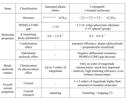
two categories as shown in Table 1.1.
One is saturated alkane chains chemisorbed on Au or Hg via S atoms, which have
high HOMO-LUMO gap of ~7 eV and exhibit relatively insulating properties. The other is
π-conjugated molecules with relatively smaller HOMO−LUMO gap of 3−5 eV. Recently, it
is reported the existence of molecule-electrode chemical bond plays a crucial role on the
junction behavior. For alkanethiol based junctions, the current difference between physical
and chemical contacts can be up to three orders of magnitude, indicating the absence of a
chemical bond gives rise to an additional barrier. For π-conjugated molecules, however, the
the molecule overlap with the metal, causing a relatively higher tunneling efficiency even
without chemical bonds.
Figure 1.1 The molecules described in the text. (a) Wires; (b) hybrid molecular electronic
Table 1.1 Electronic transports between saturated alkane chains and π-bonded molecules.
Items Classification Saturated alkane chains π-bonded molecules Conjugated
Structure
HOMO-LUMO
gap ~7 eV
~3.5 eV (oligo-phenylene ethylene) ~5 eV (phenyl group)
β (tunneling
decay parameter) 0.6 ~ 1.0 Å-1 0.2 ~ 0.6 Å-1
Conformation
effect -
transport efficiency: planar (delocalized) > perpendicular (localized) Molecular
properties
Substituted
molecule effect - Negative differential resistance, HOMO-LUMO gap decrease
Metal- molecule contact Chemicontact (or physicontact) effect
Up to 3 orders of magnitude
Only an order of magnitude - chemicontact: much less important - relatively high tunneling efficiency even
without chemicontact
Current - 1-1.5 orders of magnitude higher than
saturated (σ-bonded) molecules Overall
current
properties Current
transport tunneling Tunneling + hopping (?)
Possible conduction mechanisms through organic molecules can be deduced based on
temperature-dependent current-voltage (I−V) characteristics as described in Table 1.2.3
According to the thermal dependence of the device, conduction mechanism can be divided
into two categories. One is thermionic or hopping conduction, which has temperature
dependent I−V characteristics. The other is direct tunneling (V < ΦB/e) or Fowler-Nordheim
tunneling (V > ΦB/e), which does not have temperature dependent I−V characteristics.
Table 1.2 Possible conduction mechanisms.
Conduction
mechanism Characteristic behavior Temperature dependence dependence Voltage
Direct
tunneling 2 )
2
exp(− Φ
≈V d m
J
h none J ≈V
Fowler- Nordheim
tunneling 3 )
2 4 exp( 2 / 3 2 V q m d V J h Φ − ≈ none V V J 1 )
ln( 2 ≈
Thermionic
emission )
4 / exp( 2 T k d qV q T J B πε − Φ − ≈ T T J 1 )
ln( 2 ≈ ln(J)≈V1/2
Hopping
conduction J Vexp( kBT)
Φ − ≈ T V J 1 )
ln( ≈ J ≈V
These two tunneling mechanisms can be distinguished by voltage dependencies. When the
Fermi level of the metal is aligned closely to one energy level (HOMO or LUMO), the
Simmons model4 is a good approximation method, which can be utilized to obtain the
tunneling current density through a barrier in the voltage range of V < ΦB/e given by
} ) 2 ( ) 2 ){( 4 ( 2 / 1 2 / 1 2 / 1 2 / 1 ) 2 ( ) 2 ( 2 ) 2 ( ) 2 ( 2 2 2 s qV m B s qV m B B B e qV e qV s q A
I − Φ − − Φ +
⋅ + Φ − ⋅ − Φ = α α
π h h h
where ħ is the reduced Plank’s constant, ΦB is the effective barrier height in the
metal-insulator interface, α is a dimensionless adjustable parameter and m is the mass of electron.
The adjustable parameter (α) is used to correct the simple rectangular barrier model to
account for the effective mass of the electron. By using the nonlinear least square fitting, the
1.2.2 Fabrication and Characterization of Metal-Molecule-Metal Junctions
Considerable attention has been paid to the electrical characterization of individual
molecules during the last decade to realize the molecule-based electronics. However, there
are many obstacles to impede further progress in the field of nanometer-scale electron
transport, one of which is the lack of reliable methods to bridge a chemically synthesized
nanostructure to macroscopic electronic circuits. Recently, many different approaches have
been proposed to resolve this problem. They can be broadly divided into three categories.
First is defining a nanometer-sized electrode gap through fabrication methods. Second is
utilizing scanning probe microscope such as conducting probe atomic force microscopy or
scanning tunneling microscopy. The final is assembling nanoparticles between the electrode
gaps.
Crossed wire tunnel junction: Crossed-wire junction junctions were pioneered by
Gregory6 and have been used to measure the inelastic electron tunneling spectra of the
molecular adsorbates6 as well as to study Coulomb blockade.7 Kushmerick et al. performed
the first measurements of electron transport across organic monolayers with a crossed-wire
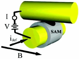
tunnel junction.8-10 A schematic representation of a crossed wire tunnel junction is shown in
Figure 1.2. The 10 µm diameter wires, one modified with a self-assembled monolayer of
interest, are mounted to a custom built test stage so that the wires are in a crossed geometry
with one wire perpendicular to the applied magnetic field (B). The junction separation is
mA). This deflection current is slowly increased to bring the wires gently together, making a
junction at the contact point.
Figure 1.2 Schematic showing the crossed-wire tunnel junction.8
All measurements are acquired in the low applied force region with constant junction
resistance. However, above a certain threshold force, the drop in resistance occurs due to the
monolayer distortion. Crossed-wire tunnel junction is considered to contain ~103 molecules.
Since a direct comparison between the measured tunneling current in the crossed-wire tunnel
junction and the tunneling current from a single molecule measured by STM shows a factor
of 103 difference,9 it has been suggested that the overall conductance of a set of parallel
conjugated molecules is a linear superposition of the individual conductances.
Thermally evaporated top contact through nanopore: Electronic measurements can
be performed in a nanostructure that has a metal top contact, a self-assembled monolayer
(SAM) active region, and a metal bottom contact as shown in Figure 1.3.5,11-13 The essential
feature of this fabrication process is the use of a nanoscale device area, which gives rise to a
defect mechanisms that hamper through-monolayer electronic transport measurements.
Figure 1.3 Schematics of a nanometer-scale device with a nanometer-scale pore etched
through a suspended silicon nitride membrane showing a Au-SAM-Au junction formed in the pore area.12
The starting substrate for the device fabrication is a 250-um-thick double-side polished
silicon (100) wafer, on which 50 nm of low-stress Si3N4 is deposited by low pressure
chemical vapor deposition. On the back surface, the nitride is removed in a square 400 µm
by 400 µm by optical lithography and reactive ion etching (RIE). The exposed silicon is
etched in an orientation-dependent anisotropic etchant (at 85 oC in a 35 % KOH solution)
through to the top surface to leave a suspended silicon nitride membrane 40 µm by 40 µm.
And then 1000 Å of SiO2 is thermally grown on the Si sidewalls to improve electrical
Au contact of 200 nm thickness is evaporated onto the top side of the membrane, filling the
pore with Au. The sample is then immediately transferred into a solution to self-assemble.
As soon as the SAM layers are formed, the sample are quickly loaded into a vacuum
chamber, and mounted onto a liquid nitrogen cooling stage to evaporate the bottom Au
electrode, in which 200 nm of Au is evaporated at 77 K at a rate of less than 1 Å/s. Negative
differential resistance (NDR) behavior was observed using a molecule containing a
nitroamine redox center as the active self-assembled monolayer in the nanopore device.11,12
Since the temperature dependent current-voltage measurements were possible using the
nanopore device, the intrinsic conduction mechanisms were investigated and inelastic
electron tunneling (IET) spectra were observed and analyzed.5
Mercury drops: Eelectron tunneling experiments were performed using
Hg-SAM/SAM-Hg or Hg-SAM/SAM-M′ junctions,14-17 where M′ is a flat metal surface. Since
mercury is a liquid metal with high affinity for thiols, these junctions have several
advantages: (i) They are relatively easy to assemble and mechanically stable. (ii) They allow
statistically large numbers of measurements. (iii) They measure the currents over small but
significant areas (~1 mm2, or ~1012 molecules) of contact. (iv) The junctions can be extended
to either systems other than thiols or electrodes with different metals (Ag, Au, Cu, Hg) and
alloys. There are disadvantages of these junctions as well: (i) They do not provide the
molecular level resolution compared to STM and break junctions. (ii) They do not support
the temperature-dependent current-voltage characterization. (iii) They probably cannot be
Mechanically controlled break junction (MCB): Measurements of electronic transport
through a single molecule (or at most very few) were carried out using lithographically
fabricated mechanically controlled break junction (MCB)18-20 to provide an electrode pair
with tunable distance as shown in Figure 1.4.
Figure 1.4 Scanning electron microscope image of the lithographically fabricated break
junction.18
To obtain a contact to a single molecule from both electrodes, an electrode pair with a
distance matching exactly this length is required. This setup is mounted in a three-point
bending mechanism driven by a threaded rod. The substrate is bent to elongate the bridge
and finally broken. Then the two open ends form an electrode gap which can be adjusted
mechanically with subangstrom precision. The molecules with acetyl protection groups at
the ends are dissolved in THF. A droplet of this solution is put on top of the opened MCB.
When the molecules approach the surface of any of the gold electrodes, one of the acetyl
protection groups splits off and a stable chemical bond between the sulfur atom and the gold
shielded box under a pressure of 10-7~10-6 mbar. While the electrodes are approaching each
other from large distances, the resistance decreases exponentially with distance and then at a
certain distance, the system suddenly locks into a stable behavior indicating a
metal-molecule-metal junction. In this system, however, different types of current-voltage
characteristics, that is, symmetry or asymmetry in the I-Vs, can be observed with the same
molecule even though all contacts are chemically stable.18
Electromigration-induced break junction: A simple yet highly reproducible method to
generate two metallic electrodes with a nanometer-sized gap has been presented. The
fabrication is based on the breakage of metallic nanowires using electromigration of metal
atoms as shown in Figure 1.5.21-27 Electromigration refers to the atomic motion in a
conductor subject to large current density. The breaking process consistently produces two
metallic electrodes whose typical separation is about 1nm. The electrode fabrication process
begins with the generation of gold nanowires using conventional electron-beam lithography
and shadow evaporation. Electron-beam lithography on a PMMA/P(MMA−MAA) bilayer
resist is used to make a 200-nm-wide resist bridge suspended 400 nm above a SiO2 substrate.
Metallic nanowires are formed by evaporating 35-Å-thick chromium and 100-Å-thick gold at
± 15o angles relative to substrate normal. Finally, 35-Å-thick chromium and 800-Å-thick
gold are deposited straight down through the resist bridge to ensure the reliable bonding
between the nanowires and the gold bonding pads. Nanometer-sized gap is formed by
ramping a voltage across the wires until a sudden drop in their conductivity occurs as a result
of their breaking. The breakage of a nanowire is typically observed to occur near the region
region. Using this break junction, the measurements of electron transport through a
nanocrystal with SAM formed on gold electrodes,21 a small ensemble of a few OPE
molecules with nitro moiety,26 and single C60 molecules23 have been performed.
Figure 1.5 Field-emission scanning electron micrographs of a representative gold
nanowire (a) before and (b) after the breaking procedure. The nanowire consists of thin (~10 nm) and thick (~90 nm) gold regions.21
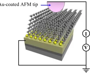
Conducting Probe Atomic Force Microscopy (CP-AFM): Metal-molecule-metal
junctions are formed by using conducting probe atomic force microscopy (CP−AFM),28-37
where a junction is fabricated by placing a conducting AFM tip in contact with a
metal-supported molecular film such as self-assembled monolayer (SAM) on Au as shown in
Figure 1.6. The normal force feedback circuit of the AFM controls the mechanical load on
the microcontact while the current-voltage characteristics are monitored. The ability to
control the load on the microcontact is the unusual characteristics of this type of junction.
The load-dependent tip-SAM contact area in these junctions is small (or order 10 nm2). This
than 100 for a 50 nm radius probe.
Figure 1.6 Scheme of the conducting probe atomic force microscopy experiment.
Voltages are applied to the tip; the substrate is kept at ground. Measurements are performed in air.
A key advantage of CP-AFM for junction formation is that no micro- or nanofabrication
processes are necessary and also molecules may be contacted by any conducting film that can
be coated onto an AFM tip, providing flexibility for investigating the role of contacts on the
junction I−V behavior. Compared to STM, CP-AFM allows the probe to be controllably
positioned just in contact in with the monolayer using an independent feedback signal,
namely normal force. The load and length dependence of electron tunneling through a SAM
of interest have been investigated.28-30,33
Scanning Tunneling Microscopy (STM): The ability to probe individual molecules
with atomic precision makes the STM an ideal tool for studying molecular electronics.38-42
However, there exist some differences between the CP-AFM method and STM for
characterizing molecular junctions. In STM, current, not force, is used to control
tip-I
V
positioning. If the STM tip is not in contact with the monolayer, the electron tunneling
properties through the junction are determined by the molecules and the vacuum (or air) gap
between the molecules and the tip. If the tip penetrates the monolayer, it is difficult to figure
out how far it has penetrated and thus what portions of the molecules contribute to the current.
The electron tunneling properties of a single-molecular junction can be measured using STM
when isolated single molecules are formed in the SAM matrix. Because there exists the
change in the STM heights caused by the thermal motion of molecules at room temperature,
STM is used after cooling down the sample to prevent the thermal motion.
Nanoparticle/Molecule/Nanoparticle Assemblies between the electrodes: Although
various methods have been reported to measure the conductance of molecular junctions,
there still remain some difficulties, which include the uncertainty about the number of
molecules in the junction and the lack of information about the shape and structure of the
metal-molecule contacts. Recently, the dimer-based contact method is presented to measure
the conductance of single conjugated molecules and provide several advantages as reported
by Dadosh et al.43 (1) metal-single molecule contact can be fabricated with high certainty.
(2) The need to fabricate nanometer-sized gaps can be avoided. (3) The temperature
dependent current-voltage characteristics can be allowed over periods of hours and even days.
Preparation method of molecularly bridged metal nanoparticles has been reported by several
groups.21,22,43-46 The electrodes are fabricated on an electron beam defined pattern, consisting
of Au/Ni layers. Electrostatic trapping method can be utilized as one of the techniques to
success rate of 50 % and show stable contact properties even over a period of a few
hours.43,47,48
1.2.3 Assembly of Particles between the Electrodes
To obtain electron transport characteristics through metal-molecule junctions,
nanoparticles (or molecularly bridged nanoparticles) can be assembled onto the electrode
gaps with (or without) functionalized SAMs using various trapping methods driven by (i)
radiation force from photon momentum change, (ii) dragging force of withdrawing meniscus
water, (iii) magnetic field gradients, and (iv) electric field gradient.
Optical trapping: The optical trapping/manipulation of single microparticles was first
demonstrated by Ashkin in 1970.49 Optical trapping/manipulation is sometimes referred to as
laser trapping/manipulation or optical/laser tweezers.50-56 A basic principle of optical
trapping of a single microparticle is the refraction of a focused laser beam through the
particle, as shown schematically in Figure 1.7.
The refraction of light induces a photon momentum change, since the propagation direction
and the wavelength of light vary in media with different refractive indices. The change in the
light momentum, ∆P = P1− P2 where P1 and P2 are the momentum before and after refraction,
respectively, should be conserved, so that a force is exerted on the particle with a direction
opposite to that of the momentum change: -∆P. When the refractive index of the particle (np)
is larger than that of the surrounding medium (nm), the net force generated by the laser beam
is directed to the focal point of the beam: f in Figure 1.7. This force is called “radiation
force” or “radiation pressure”, and acts as the driving force for optical trapping. Under the
condition np < nm, however, a particle experience the repulsive force from the laser beam.
One technical method to trap such particles is the scanning laser micromanipulation, which is
fast and repetitive circular scans of a focused laser beam around a particle to be trapped (or
“encaged”). In addition to particles with np < nm, metal particles with high reflection and/or
absorption coefficient at the wavelength of the incident light also experience repulsive forces
from it. Metal particles such Au, Ag, and Cu can be trapped optically by a TEM01-mode laser
beam with an intensity minimum on the beam axis as well as the scanning method.
Receding meniscus: The effort to precisely position (bio)molecules onto
microstructured substrates has been made using a receding meniscus generated by a drying
droplet.57-59 Receding meniscus method allows DNA molecules to be aligned and also
avoids the possible damage during fabrication (e.g., metallization prior to electrical
measurement). Chu et al.60 in our group assembled the nanoparticles onto a
force of withdrawing meniscus water. Therefore, the electron transport measurements of the
molecules of interest are possible using SAM-nanoparticles-SAM bridge structure between
the electrode gaps.
Magnetic directed assembly: A magnetic directed-assembly technique was reported to
make molecular junctions based on magnetically susceptible and electrically conductive
microspheres46 and also to fabricate carbon nanotube field-effect transistors61 between
magnetic source/drain electrodes. Magnetic directed assembly utilizes localized magnetic
fields within a ferromagnetic array to direct magnetically susceptible species to the high-field
region between micro-scale electrodes. Magnetic directed assembly has several desirable
properties in terms of device fabrication such as high yield, accurate placement, and
predictable orientation for assembled species. Fabrication procedure is shown in Figure 1.8.
Figure 1.8 (a) Illustration showing the fabrication of hemispherically metallized silica
microspheres and their magnetic controlled assembly onto SAM-functionalized electrodes. (b) SEM image showing such a microsphere junction.51
(a)
The assembly efficiency shows that approximately 60 % of junctions exhibit single bead,
20-30 % show two to three beads, and 10-20 % remain empty.46 In terms of contact stability,
it is found that the I−V characteristics are reproducible over several days and also are able to
stand up to applied bias of 2 V. Magnetic-directed assembly is suggested to provide a simple
method for the parallel fabrication of molecular junctions.
Electrostatic trapping: The movement of polarizable particles in non-uniform fields,
termed dielectrophoresis by Pohl,62 has been utilized as a useful invasive,
non-destructive tool for separation of micro-organisms62,63 and trapping of nanoparticles43,44,64-77
and carbon nanotubes.78-84 The basic principle of dielectrophoresis is that when placed in a
non-uniform alternating current (AC) electric field, polarized particles experiences a variable
translational force, depending on the field frequency. For a homogeneous dielectric particle
suspended in an aqueous medium, the time-averaged DEP force can be expressed as
2 3Re( )
2 )
( mr fCM Erms
F ω = πε ∇
where ω is the angular field frequency, r is the particle’s radius, fCM is the Clausis-Mossoti
factor given by
* * * * 2 m p m p CM f ε ε ε ε + − =
where *
p
ε and *
p
ε is the complex permittivities of the particle and the medium, respectively.
For a real dielectric, the complex permittivity is
ω σ ε
where j= −1, ε is the permittivity and σ is the conductivity of the dielectric. From
equation (1), the absolute value of DEP force depends on the term ∇Erms 2, (a factor related
to the geometry of the electric field) and on the real part of fCM, the in-phase component of
the particle’s effective polarizability. The real part of fCM is bounded by the limits
2 1 ) Re(
1< fCM <− and varies with the frequency of the applied field and the complex
permittivity of the medium. Positive DEP occurs when Re(fCM)>0, the force is towards
regions of highest field strength. However, when Re(fCM)<0 , the force is towards
decreasing field strength and the particles are repelled from the electrode edges. The
direction of DEP force is shifted at the crossover frequency at which the Clausis-Mossotti
factor crosses from positive to negative. Dielectric constants of various materials are given
in the table 1.3 below.
Table 1.3 Dielectric constants of various materials.
Materials water cyclohexane Aceton Ethanol Polystyrene Metals
Dielectric constant 80 2.03 21 26 2.55 ∞
In case of metal nanoparticles in aqueous medium, Re(fCM)~1, indicating that positive DEP