Design and Implementation of Small -Signal
model Single-Phase DVR for Voltage Sag
Compensation
P.Madasamy
1, K.Ramadas
2Assistant Professor, Department of Electrical and Electronics Engineering, Alagappa Chettiar College Engineering
and Technology, Karaikudi, Tamilnadu, India 12
ABSTRACT: In this paper, compensation of Voltage sags/swells by small signal design of a single phase DVR using PID controller is proposed. Voltage sags are sudden voltage reduction that may be present among power systems. It persists from milliseconds to a minute of duration. Different causes may produce voltage sags such as lightning, presence of non-linear equipment connected to the power grid or presence of short circuit faults. Sensitive loads, like electronic equipments, may be damaged or present malfunctioning during the voltage sag, generating economical losses. A suitable solution to compensate this voltage disturbance is the Dynamic Voltage Restorer (DVR). It is power electronics- based solution that provides power compensation to sensitive loads during the sag occurrence. The DVR must operate with control loops, monitoring the load voltage and generate the compensation during the sag. Those control loops must be tuned with aid of a mathematical model, a performance criteria and a proper design procedure of the controller. A small-signal equivalent circuit will be obtained and its analysis will produce the control-to-output transfer function. Using the control-to-output transfer function a PID voltage controller will be designed. This PID design methods will be described and the proper operation will be verified through mat lab simulation and the hardware results of the developed small signal model single phase DVR are explained.
KEYWORDS:Voltage sag, DVR, PID Voltage controller, small signal equivalent circuit.
I. INTRODUCTION
There is an increasing need for renewable energy systems (RES) with ancillary features particularly in low voltage distribution systems. Ancillary features include harmonic compensation, reactive power compensation, low voltage ride through capability etc. This is due to the fact that there is increased penetration of nonlinear power electronics based loads. These loads inject harmonic currents into grid which can cause distortion at point of common coupling (PCC) particularly in weak grid systems. Moreover, due to the intermittent nature of the clean energy sources such as wind and solar energy, their increased penetration lead grid voltage fluctuations depending upon power generation and demand. These voltage fluctuations can affect sensitive power electronic loads such as adjustable speed drives, lighting systems etc which can lead to frequent tripping, mal operation and thus leading to increased maintenance costs.
duration. According to the IEEE 1159 – 1995 the voltage sag is a decrease of voltage RMS value that varies between 0.1pu to 0.9pu and may occur during 0.5 to 30 cycles. This disturbance causes economical problems due the use of electronic and microprocessor based equipments that are susceptible to fail or be damaged by this abrupt voltage decrease. Even voltage sags with short duration may cause equipment restarting or damage and generate economical losses. An efficient mitigation technique is achieved by the use of Dynamic voltage restorers (DVR). They are usually formed by a voltage source inverter which output is connected to a low- pass filter and an injection transformer. The purpose of the injection transformer is to provide electrical isolation between the voltage grid and the dc-ac converter, but there are topologies that exclude its use. This is because the transformer can be heavy, bulky and expensive.
At the voltage source inverter DC bus there is an energy bank that provides a constant voltage. This energy bank may be formed by huge energy storage components like Lead-acid batteries banks, Flywheels, Super Capacitors or even photovoltaic cell banks, but there exists self-supported solutions where the DC bus voltage is self-regulated by the action of the DVR control loop. The voltage compensation is generated by the DVR through a control loop that monitors the load voltage and produces the compensation through a specified strategy based on a mathematical analysis and a control law that aims to achieve the specified stability and performance criteria. By the small-signal modeling, the effective mathematical analysis may be determined and the system dynamic behavior can be represented by an equivalent electric circuit. Through the equivalent circuit analysis, the system control-to-output transfer function a and the DVR output voltage controller can be designed. This paper presents a small-signal modeling of a single- phase transformer less DVR. The analysis of the small-signal model will determine the equivalent control-to-output transfer function, whose frequency response will be used to design a PID controller. The performance of the DVR will be evaluated through computer simulation.
II. SYSTEM DESCRIPTION
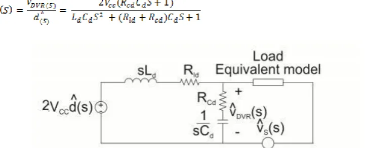
A. DVR POWER SCHEME
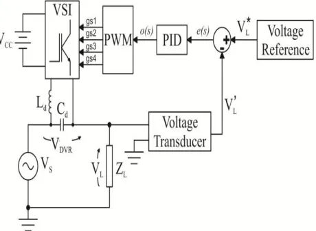
The discussed DVR system is illustrated at Fig. 1. It is composed by a single-phase full bridge voltage source inverter (VSI) formed by IGBTs. There is a constant voltage VCC at the VSI dc bus that will provide the power
compensation during the voltage sag. A low-pass filter is connected at the VSI output. This passive filter is composed by the inductor Ld and a capacitor Cd and is designed to eliminate high frequency harmonic voltages
that are appear at the VSI output.
L
L
L
L
The voltage VDVR across the capacitor Cd is the DVR output voltage. The DVR output is connected between the
power supply VS and the load ZL.
A. Control strategy
The control strategy is also illustrated at Fig. 2. At first, the load voltage VL is measured by a voltage transducer
and the signal V' is generated. This signal is compared with the voltage reference V*. The resultant error e(s) goes in the PID controller block that will produce the output o(s) that is used by the PWM block to generate the gate signals (gs1 to gs4) and command the IGBTs.
B. Voltage Reference considerations
The reference signal V* is very important for the proper DVR operation. This signal must be sinusoidal and in phase with the power supply Vs. The use of PLL circuits is very common in DVRs for the proper synchronization
of Vs and V* [8]. In this paper will be considered that the reference voltage is already in phase with the power
supply voltage.
C. Modes of operation
When the voltage sag occurs the DVR must supply the real power from the stored energy together with the reactive power requirement for the voltage compensation. Even if the amplitude difference is short, the power may assume high quantities. Thus the voltage amplitude compensation is achieved by injecting reactive or real power from the DVR . The analyzed DVR system operates in an in phase compensation mode. In this mode the DVR compensates only the voltage amplitude. The compensated voltage has the same phase as the sagged voltage, [8]. According to [8] this technique minimizes the voltage injected by the DVR and is suited for the linear loads which do not need phase angle compensation.
III.DVR BASICS OPERATION
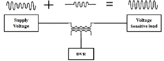
A Dynamic Voltage Restorer is a lately proposed series connected solid state device that injects missing voltage waveform into the system for regulating the voltage at the load end. Its location in the distribution system is between supply and sensitive load. It continuously and quickly regulate the load side voltage in case of any power quality issues like voltage sag or swell thus preventing any power interruption to the sensitive load. There are different methodologies and control techniques by which a DVR can be implemented. A. Operating Principle The fundamental principle behind DVR operation is that it injects a voltage waveform through an injection transformer that is the difference between pre-sag and sagged voltage.
This is demonstrated in Fig. 1.1.This is made possible by the supply of required real/active power from an energy storage device along with reactive power. The injection transformer ratio and ratings of the energy storage device can put limitations on the maximum injection capability of DVR.
3.1 Operating Modes of DVR
The operating modes of DVR can be classified into three as below:
a) Protection mode:
In case of short circuit fault on load and high inrush current, the over current on the load side exceeds an allowable limit. Then the DVR will get cut off from the systems by using the bypass switches and providing alternate path for current flow.
b) Standby mode:
Switching of semiconductors of VSI will not occur in this mode and the full load current will pass through the primary winding of injection transformer. The low voltage winding of the injection transformer is shorted through the converter in this mode.
c) Injection mode:
DVR injects voltage through the injection transformer to compensate for any disturbance detected in the supply voltage.
IV.PROPOSED DVR BLOCK DIAGRAM
Figure 4.1 Block diagram of Proposed DVR
V. SMALLSIGNALANDSYSTEMTRANSFERFUNCTIONS
A.DYNAMIC VOLTAGE RESTORER OPERATION
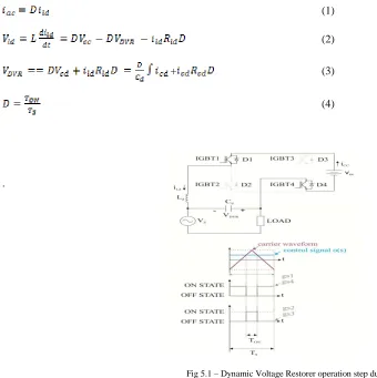
This paper proposes control of Voltage sags/swells by small signal designing of a single phase DVR using PID controller. Useful transfer functions are obtained through the small-signal modelling of the DVR system. This modelling approach extracts the average value of inductor voltages and capacitor currents during a switching period. It is assumed that the PWM block operates with an analog pulse width modulation where the gate signals (gs1 to gs4) are generated by the result of comparing a triangular carrier waveform and the control signal. During the period TON is a part of the switching period TS where the carrier waveform is greater than the control signal and a pair of MOSFETs will conduct. This is shown at Fig. 3.1 which analysis generates expressions (1) to (4).
(1)
(2)
+ (3)
(4)
.
Fig 5.2 - Dynamic Voltage Restorer operation step during TOFF.
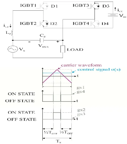
At the end of TON the MOSFETs stop to conduct. Due the stored energy of Ld, the diode pair D2 and D3 starts to conduct and the operation step is shown at Fig. 3.2. The analysis of this generates the expressions (5) to (8).
(5)
(6)
+ (7)
(8)
Vol. 3, Issue 7, July 2014
Considering the expression (9) it will be assumed that the DVR output voltage
VDVR and currents iLd and Icc will also be represented by a constant value (dc term) super imposed by a small signal (ac term), as shown in (10) to (12).
Using the procedure , expressions (1) to (12) the small-signal equivalent electrical circuit model is obtained.
3.2 CONTROL-TO-OUTPUT TRANSFER FUNCTION
The control-to-output transfer function is expressed at (13) and is obtained by the analysis of circuit in Fig 3.3. This transfer function relates small variations of DVR output voltage VDVR (s) with small variations of the control signal d(s).
Fig. 5.3 Small signal model of the DVR (simplified small-signal model)
VI. SIMULATIONRESULTANDDISCUSSION
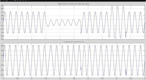
In this simulation results,
Input voltage =300v
Vol. 3, Issue 7, July 2014
Swell voltage (500v) occurs at the time duration between t=0.37 to 0.43s (3 cycles) And its compensated output voltage = 300 v .
Input and output voltages are shown in the figure 4.3 below
Fig 6.1 Single phase DVR simulation outputs
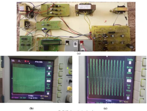
VII. HARDWARE IMPLEMENTATION
Input single phase 230v, 50 Hz supply is given to the single phase DVR hardware circuit through single phase auto transformer. Set input voltage (48v) using auto transformer. If varying autotransformer voltage below 46v, considered as sag occurs in input supply and Single phase DVR injects voltage ,to maintain (48v) constant output voltage. If varying autotransformer above 50v, considered as swell occurs in input supply and single phase DVR absorbs voltage, to maintain (48v) constant output voltage.
The controller generate control signals based on sag/swell for compensating for varying turn on and turn off time of the inverter circuit, to maintain constant output voltage irrespective of sag and swell occurs.
Vol. 3, Issue 7, July 2014
(a)
(b) (c)
Fig 7.1 Hardware circuit and results
Table. Results of proposed method
Input voltage Sag/swell voltage and Time Duration
/Cycles Output voltage
Simulation circuit
Vi=300v
Sag voltage=100 v t=0.25 to 0.27s(6 cycles)
Swell voltage=500v t=0.37 to 0.43s (3 cycles)
Vo=300v
Hardware circuit
Vi=48v
Sag voltage=46v t=200 to 450ms
(19 cycles)
Vol. 3, Issue 7, July 2014
VIII. CONCLUSION
This paper presented a design of a small signal model single phase dynamic voltage restorer. That model allowed representing the dynamic characteristics in an equivalent circuit. This circuit analysis generated transfer functions that were useful to design a PID controller responsible to control the DVR output voltage. Simulation results confirmed the expected DVR performance because it was able to restore the load voltage amplitude when voltage sag occurs. With this model, we able to compensate sag and swell voltages occur in power supply. This proposed Hardware circuit design has been based on the PIC controller, which ensures to compensate the voltage sag and swell.
REFERENCES
[1] asuni Perera, Daniel Salomonsson, Arulampalam Atputharajah, and Sanath Alahakoon, "Automated Control Technique for a Single Phase Dynamic Voltage Restorer," in 2006 International Conference on Information and Automation, Shandong, 2006, pp. 63-68. [2] Ambra Sannino, Michelle Ghans Miller, and Math H.J. Bollen, "Overview of Voltage Sag Mitigation," in IEEE Power Engineering
Society Winter Meeting, 2000. , 2000, pp. 2872 - 2878.
[3] B.H Li, S.S. Choi, and D.M. Vilathgamuwa, "Transformerless dynamic voltage restorer," IEE Proceedings - Generation, Transmission and Distribution , vol. 149, no. 3, pp. 263 - 273, May 2002.
[4] Carl Ngai-man Ho, Henry S.H. Chung, and Keith T.K. Au, "Design and Implementation of a Fast Dynamic Control Scheme for Capacitor- Supported Dynamic Voltage Rstorers," IEEE Transactions on Power Electronics, vol. 23, no. 1, pp. 237-251, January 2008. [5] Sidelmo M. Silva, Sandro Élisson Silveira, André de Souza Reis, and Braz J. Cardoso Filho, "Analysis of a Dynamic Voltage
Compensator with Reduced Switch-Count and Absence of Energy Storage System," IEEE Transactions on Industry Applications, vol. 41, no. 5, pp. 1255- 1262, September/October 2005.
[6] Arindam Ghosh, Amit Kumar Jindal, and Avinash Joshi, "Design of a Capacitor-Supported Dynamic Voltage Restorer (DVR) for Unbalance and Distorted Loads," IEEE Transactions on Power Delivery, vol. 19, no. 1, pp. 405-413, January 2004.
[7] Eng Kian Kenneth Sng, S.S. Choi, and D. Mahinda Vilathgamuwa, "Analysis of Series Compensation and DC-Link Voltage Controls of a Transformerless Self-Charging Dynamic Voltage Restorer," IEEE Transactions on Power Delivery, vol. 19, no. 3, pp. 1511-1518, July 2004.
[8] Ali Yazdanpanah Goharrizi, Seyed Hossein Hosseini, Mehran Sabahi, and Gevorg B. Gharehpetian, "Three-Phase HFL-DVR with Indenpendently Controlled Phases," IEEE Transactions on Power Electronics, vol. 27, no. 4, pp. 1706-1718, April 2012.
[9] Enio Roberto Ribeiro and Ivo Barbi, "Harmonic Voltage Reduction Using a Series Active Filter Under Different Load Conditions," IEEE Transactions on Power Electronics, vol. 21, no. 5, pp. 1394-1402, September 2006.
[10] Robert W. Erickson and Dragan Maksimovic, Fundamentals of power electronics, 2nd ed. New Delhi: Springer, 2001. [11] Charles L. Phillips and Royce D. Harbor, Feedback control systems. New Jersey: Prentice Hall, 1996.