ABSTRACT
JUMADE, RAGHAV JAYANT. Study of Magnetic Domain Wall Dynamics for Memory and Logic Implementation. (Under the direction of Dr. Veena Misra.)
With conventional CMOS scaling approaching its end, implementations of logic
and memory in non-conventional technologies have become focus of research. Logic
schemes based on motion of magnetic domains in ultra-thin ferromagnetic films have been
anticipated to offer probable low-power, non-volatile alternative to CMOS design. Speed
of magnetic domain walls has been found to be low and unlike motion of electrons (or
holes), the motion of magnetic domain walls is not very well understood. This report
presents scrutiny of dynamics of magnetic domain walls in order to bring out design goals,
limitations and various trade-offs in this technology. Motion of magnetic domain walls in
Permalloy (N i80F e20) nanowires caused by application of both external magnetic field and
electric current is the focus of this thesis. In this document, effect of material parameters
like saturation magnetization (MS) and Gilbert damping factor (α) on velocities of
magnetic domain walls has been illustrated. These parameters also affect the Walker
Breakdown process and this development has also been presented. Similarly, effect of
nanowire dimensions on their speed characteristics has also been analyzed. In addition
to these, simulations showing consequence of increasing amounts of non-adiabatic spin
torques are also performed. Using each of these simulations, pattern between variation
of Walker Breakdown point, critical current density (or field), mobility, etc. and the
controlling parameter (magnetization, damping, nanowire dimension or non-adiabaticity)
can be developed. These simulations are also extended to nanowires with Perpendicular
Magnetic Anisotropy (PMA). The relationships obtained in simulations described above
logic gates using Co/Pt multi-layer PMA nanowires. All nanowire devices are simulated
using nmag-0.1 and rings are simulated using OOMMF. Simulations are used to assess
performance of designed memory and logic devices and compared to existing CMOS
technology. These comparisons based on our simulations reveal that logic and memory
implementations based on motion of magnetic domain walls provide higher functional
density and lower power consumption than CMOS implementations. These advantages
are obtained at the cost of speed of operation. Low power and higher density along with
non-volatility imply that this technology can be a great aid for embedded data processing
c
Copyright 2010 by Raghav Jayant Jumade
Study of Magnetic Domain Wall Dynamics for Memory and Logic Implementation
by
Raghav Jayant Jumade
A thesis submitted to the Graduate Faculty of North Carolina State University
in partial fulfillment of the requirements for the Degree of
Master of Science
Electrical Engineering
Raleigh, North Carolina
2010
APPROVED BY:
Dr. John Muth Dr. Salah Bedair
DEDICATION
To
Aai and Baba
BIOGRAPHY
The author was born in a well educated family on 18 July 1986. He completed his
Bachelor’s degree in Electronics and Communication Engineering from Visvesvaraya
National Institute of Technology. He then worked in Dr. Krishnapura’s group at Indian
Institute of Technology Madras. In August 2008, Raghav started his Masters at North
Carolina State University where he worked in Dr. Misra’s group, implementing logic
ACKNOWLEDGEMENTS
Infinite stars in the sky, so few that catch the eye...
Firstly, I must thank my advisor Dr. Veena Misra for creating the opportunity for me
to work on this project. I am grateful to her for her unrelenting support, interest and
critique throughout this work. I am also honored to have Dr. Muth and Dr. Bedair on
my graduate committee. I greatly value their suggestions which helped me improve this
work.
My group members helped me sustain the most barren of times and to enjoy the
packets of success. I appreciate the help I received from Rebecca, Rahul, Steven, Srikant,
Smita, Xiangyu, Jason and Casey. The discussions and debates I had with them were
most educating and entertaining.
I must also thank my room-mates Nikhil and Bhushan for putting up with my quirks.
If not for their culinary skills, American fast-food would have claimed another soul. I
am indebted to my friends - Saket, Nandu and Prashanth, for directing me towards the
decisions I made.
Most importantly, I grab this opportunity to thank my loving parents, Vandana
and Jayant, for maintaining faith in me and supporting me throughout. I run short of
words and action to express my gratitude towards them. I am also thankful to my little
sister Anushree for being my eyes and ears back home. I thank my family for being the
ubiquitous guiding force in my life.
I extend my gratitude and sincere apologies to all others, and there are many, who
TABLE OF CONTENTS
List of Tables . . . viii
List of Figures . . . ix
Chapter 1 Introduction . . . 1
1.1 Background . . . 1
1.2 Concepts and Definitions . . . 3
1.2.1 Magnetic Materials . . . 3
1.2.2 Characteristic Features of Magnetic Materials . . . 4
1.2.3 Magnetic Domain Walls . . . 5
1.2.4 Theory of Magnetism . . . 6
1.2.5 Energies in Magnetic Theory . . . 6
1.3 Objective . . . 7
References . . . 8
Chapter 2 Domain Wall Motion under Magnetic Field . . . 11
2.1 Nature of Domain Walls in Nanowires . . . 12
2.2 Velocity of Domain Wall Motion . . . 18
2.2.1 Typical Domain Wall Speed Characteristics . . . 20
2.2.2 Effect of Domain Wall Structure . . . 22
2.2.3 Effect of Nanowire Dimensions . . . 24
2.2.4 Effect of Gilbert Damping Constant ‘α’ . . . 24
2.2.5 Effect of Saturation Magnetization ‘MS’ . . . 28
2.3 Improving the performance of Nanowires . . . 29
2.3.1 Application of Roughness . . . 30
2.3.2 Effect of Transverse Magnetic Field . . . 34
2.4 Summary . . . 40
References . . . 42
Chapter 3 Electric Current Driven Domain Wall Motion . . . 44
3.1 Motivation . . . 44
3.2 Concept of Spin Torque Transfer (STT) . . . 45
3.2.1 Adiabatic Spin Torque Transfer . . . 48
3.2.2 Non-adiabatic Spin Torque Transfer . . . 49
3.3 Velocity of current Driven Domain Wall Motion . . . 50
3.3.1 Effect of Cross Section of the nanowire . . . 51
3.3.4 Effect of Non-adiabaticity ‘β’ . . . 59
3.3.5 Effect of Transverse Magnetic Field . . . 62
3.4 Summary . . . 65
References . . . 67
Chapter 4 Perpendicular Magnetic Anisotropy . . . 69
4.1 Critical Current for Domain Wall Motion . . . 69
4.2 Speed of Magnetic Domain Walls in PMA . . . 71
4.2.1 Effect of Nanowire Width . . . 71
4.2.2 Effect of Saturation Magnetization . . . 73
4.2.3 Effect of Damping Coefficient . . . 77
4.2.4 Non-adiabatic Domain Wall Motion . . . 77
4.3 Device Performance and type of DW Motion . . . 80
4.3.1 Motion of Multiple Domain Walls . . . 83
4.4 Summary . . . 88
References . . . 89
Chapter 5 Implementation of Memory and Logic . . . 90
5.1 Background: Search for Universal Memory . . . 90
5.1.1 Ferromagnetism as Storage Mechanism . . . 91
5.1.2 Ferromagnetic Properties for Implementing Memory . . . 93
5.2 Magnetic Properties of Rings . . . 93
5.2.1 Circular Rings . . . 94
5.2.2 Elliptical Rings . . . 96
5.2.3 Rhombus Rings . . . 98
5.3 Possibility of Logic Scheme . . . 100
5.3.1 MQCA . . . 102
5.3.2 Domain Wall Logic . . . 103
5.3.3 PMA Inverter . . . 103
5.4 Study of Nucleation Field . . . 104
5.4.1 Effect of Saturation Magnetization . . . 107
5.4.2 Effect of Cross-section of Nanowire . . . 107
5.5 Study of Dipolar Field . . . 107
5.5.1 Effect of Saturation Magnetization . . . 109
5.5.2 Effect of Gap between Nanowires . . . 109
5.6 Improved PMA Inverter . . . 109
5.6.1 Other Logic Gates . . . 111
5.7 Summary . . . 116
Chapter 6 Conclusions and Future Work . . . 118
6.1 Comparison with CMOS Technology . . . 118
6.1.1 Comparison of Speed . . . 118
6.1.2 Comparison of Power . . . 119
6.2 Achievements of this Thesis . . . 120
LIST OF TABLES
LIST OF FIGURES
Figure 2.1 Structure of (a) Bloch Wall and (b) Neel Wall. . . 13 Figure 2.2 Difference between in-plane walls. (a) Transverse Wall and (b)
Vortex Wall. . . 13 Figure 2.3 Changing shape of the domain wall as width of the nanowire is
increased. Nanowire widths for (a)-(d) are 10nm, 30nm, 50nm and 100nm respectively. . . 15 Figure 2.4 Variation of length of domain wall (∆) with width of nanowire for
various nanowire thicknesses. . . 17 Figure 2.5 Variation of length of domain wall (∆) with thickness of nanowire
(Width = 100nm). . . 17 Figure 2.6 Device geometry used to obtain domain wall velocity from
magneti-zation curve. . . 19 Figure 2.7 Change in net magnetization of a nanowire due to motion of
mag-netic domain wall. . . 19 Figure 2.8 Typical DW Speed v/s Applied Field Curve: Figure shows the
nature of domain wall in pre and post Walker Breakdown regions. 21 Figure 2.9 Magnetization curves of nanowires with different cross-sections
under external applied field of 10Oe: (a)N W1 is 10×10nm2 while (b) N W2 is 20×10nm2. . . 23 Figure 2.10 Plot showing change in average domain wall velocity with applied
magnetic for nanowires having thickness 10nmand different widths. 25 Figure 2.11 Plot showing the effect of width of nanowire (thickness = 10nm)
on the field at which Walker Breakdown occurs in it. Figure also shows the effect of width of nanowire on maximum velocity reached before Walker Breakdown. . . 25 Figure 2.12 Variation in domain wall velocity - magnetic field curves of nanowire
(50×10nm2 in cross-section) with change in damping coefficient of the material. . . 27 Figure 2.13 Variation of peak velocity with Gilbert damping of the nanowire.
Red line indicates the fitting with curve of the form y=A/(x−x0). 27 Figure 2.14 Variation of Magnetization curves with change in saturation
magne-tization MS of the nanowire (50×10nm2 in cross-section) material. Inset shows variation of the point of Walker Breakdown due to change in saturation magnetization. . . 29 Figure 2.15 Definition of edge roughness in a Permalloy nanowire. Depth ’d’ in
Figure 2.16 Magnetization curves of rough permalloy nanowire of cross-section 20nm×10nm. Different traces refer to different seeds used for ran-domization. (a) has higher magnitude of roughness (d0 = 0.25nm) compared to (b) withd0 = 0.1nm. . . 32 Figure 2.17 Variation of speed of magnetic firld driven domain wall motion in
rough nanowires. Each curve relates to different amount of added roughness. . . 34 Figure 2.18 Figure shows variation of Walker Breakdown field HW B and speed
vW B with magnitude of roughness added to a smooth nanowire. . 35 Figure 2.19 Figure showing domain speedv v/s external longitudinal fieldHlong
for increasing amounts of transverse magnetic fields. For all of these, transverse field is in the same direction as the domain wall. . . 36 Figure 2.20 Variation of the change in point of Walker Breakdown (δHW B,δvW B)
with applied positive transverse field. This plot can be divided into three distinct zones HT rans < 60Oe, 60Oe < HT rans < 150Oe,
HT rans >150Oe. . . 36 Figure 2.21 Variation of the change in point of Walker Breakdown (δHW B,
δvW B) with transverse field applied opposite to the direction of domain wall. . . 38 Figure 2.22 Variation of the change in point of Walker Breakdown (δHW B,
δvW B) with transverse field applied out of plane of the nanowire. Figure makes it clear that amount of improvement obtained is lower than the situation where transverse field is in plane of the nanowire. 39
Figure 3.1 The relative orientation of spin-torque and damnping force which leads to precession of atomic magnetic moments. . . 46 Figure 3.2 Phenomenon of Adiabatic Spin Torque Transfer: Figure shows the
change spin of an electron when it crosses the domain wall. . . 47 Figure 3.3 Process of Non-adiabatic Spin Torque Transfer: Figure shows
re-flection of a spin polarized electron at the magnetic domain wall. . 50 Figure 3.4 Figure shows change in domain wall speed with respect to Spin
velocity for nanowires of varying widths. Spin velocity is the measure of current passing through the nanowires. ’u’ in these figures can be replaced by ‘J’ using scaling factor of 1.38×10¹⁰. . . 51 Figure 3.5 Variation of critical spin velocity with respect to width of the
Figure 3.6 Variation of the point of Walker Breakdown with width of the wire. ‘uW B’ represents the maximum current that the nanowire can carry
in absence of external magnetic field before experiencing sharp degradation of mobility. Similarly, ‘vW B’ is the maximum velocity of domain wall motion before Walker Breakdown occurs. . . 53 Figure 3.7 Effect of changing Gilbert Damping on Adiabatic Current Driven
Domain Wall Motion in a nanowire of cross-section 50×10nm2. . 54 Figure 3.8 Linear relationship between critical current density (represented by
critical spin velocity) and Gilbert Damping of the nanowire. . . . 55 Figure 3.9 Variation of the point of Walker Breakdown with damping factor of
material of the wire. ‘uW B’ represents the maximum current that the nanowire can carry in absence of external magnetic field before experiencing sharp degradation of mobility. Similarly, ‘vW B’ is the maximum velocity of domain wall motion before Walker Breakdown occurs. . . 56 Figure 3.10 Domain Wall Speed versus Spin Velocity (Electric Current
Den-sity) curves of permalloy nanowire (cross-section 50×10nm2) with different values of saturation magnetization. . . 57 Figure 3.11 Variation in key features of domain wall motion with various values
of saturation magnetization MS. . . 57 Figure 3.12 Domain Wall speed plots for permalloy nanowires of cross-section
50×10nm2 and damping coefficient 0.05 at various values of non-adiabaticities. . . 59 Figure 3.13 (a) Variation of maximum electric current that can be sustained
before Walker breakdown occurs. Each curve represents different value of Gilbert damping. (b) Variation of maximum speed of domain walls reached before Walker Breakdown occurs for given value of damping coefficient. . . 61 Figure 3.14 Consequence of applying transverse field along the direction of
magnetic domain wall on its motion. Figure shows the effects of transverse field on features of domain wall motion like critical current density and Walker Breakdown. . . 64 Figure 3.15 Consequence of applying transverse field opposite to the direction
of magnetic domain wall on its motion. Figure shows the effects of transverse field on features of domain wall motion like critical current density and Walker Breakdown. . . 64 Figure 3.16 Effect of applying out-of-plane transverse magnetic field on current
Figure 3.17 Each of the features of current driven domain wall motion plotted to a proper scale to analyze the effect of magnitude of out of plane field on these parameters. . . 66
Figure 4.1 Comparison of Domain Wall dynamics in materials with in-plane and perpendicular magnetic anisotropies. PMA type nanowires show much lower critical spin velocity. . . 70 Figure 4.2 Variation of Domain Wall velocity characteristics in materials with
PMA. Simulations were done for wires with MS = 800kA/m and
α= 0.03. . . 72 Figure 4.3 Variation of features of domain wall motion, viz, critical spin velocity,
Breakdown spin velocity and domain wall speed at Walker point in materials with PMA. Simulations were done for wires withMS = 800kA/mandα= 0.03. Hollow symbols represent the resuls for IMA. 72 Figure 4.4 Impact of saturation magnetization on the characteristics of
mag-netic domain wall motion in PMA type nanowires of cross-section 50×10nm2 and α = 0.03. Hollow symbols represent the resuls for IMA. . . 74 Figure 4.5 Variation in critical spin velocity required to start adiabatic domain
wall motion in PMA type nanowires. Hollow symbols represent the results for IMA. . . 75 Figure 4.6 Variation of Walker Breakdown point with change in saturation
mag-netization. For comparison results from IMA simulations denoted by hollow symbols are also presented. . . 75 Figure 4.7 Variation in critical spin velocity required to start adiabatic domain
wall motion in PMA type nanowires as a function of Gilbert damping. Hollow symbols represent the results for IMA. . . 76 Figure 4.8 Variation of Walker Breakdown point with change in Gilbert
Damp-ing. For comparison results from IMA simulations denoted by hollow symbols are also presented. . . 76 Figure 4.9 Simulation results for non-adiabatic domain wall motion in nanowires
with PMA. Results can be compared to those from IMA type wires (hollow symbols). . . 78 Figure 4.10 Variation of current at Walker Breakdown point (represented by
uW B) with change in ration β/α. Results can be compared to those for IMA using traces with hollow symbols. . . 79 Figure 4.11 Variation of domain wall speed at Walker Breakdown point
Figure 4.12 Comparing the maximum domain wall speed obtained before Walker Breakdown. The figure shows that under adiabatic region CDDWM in IMA type wires is slower compared to both field driven and CDDWM PMA wires. . . 82 Figure 4.13 Comparison showing that the fastest motion of domain walls is
obtained in PMA nanowires under non-adiabatic situations. . . . 82 Figure 4.14 A nanowire containing more than two domains. (a) shows the way
the nanowire is defined. It also shows the definition of the term bit-length. (b) shows the domain structure of the nanowire after relaxation. Domain walls have grown to their stable sizes. . . 83 Figure 4.15 Magnetization characteristics of the nanowire when the magnetic
domain engulfed by the two domain walls remains unharmed till the end of simulation. MX is replaced by MZ in case of PMA type wires. . . 85 Figure 4.16 Magnetization characteristics of the nanowire when the magnetic
domain engulfed by the two domain walls gets destroyed during motion of domain walls. MX is replaced by MZ in case of PMA type wires. . . 85 Figure 4.17 Variation of minimum bit-length required to ensure non-destructive
transmission of data as a function of applied current density (repre-sented by uC) and Gilbert Damping. These simulations are for the case of IMA type wires. . . 86 Figure 4.18 Variation of minimum bit-length required to ensure non-destructive
transmission of data as a function of applied current density (repre-sented by uC) and Gilbert Damping. These simulations are for the case of PMA type wires. . . 87
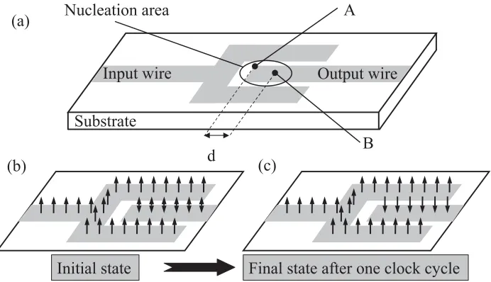
Figure 5.1 B-H Loop of a bulk ferromagnetic maerial. Figure indicates co-ercivity and remanence of the material. Remanence is directly proportional to saturation magnetization of the material. . . 92 Figure 5.2 Magnetization Characteristics of circular permalloy rings of inner
diameter 50nm and outer diameters varying between 100nm and 200nm. . . 95 Figure 5.3 Magnetization Characteristics of circular permalloy rings of outer
diameter 200nm and inner diameters varying between 0nm and 150nm. The ring with zero inner diameter is actually a disk and therefore shows peculiar magnetization curve . . . 96 Figure 5.4 Figure explaining the magnetization states of the ring at different
Figure 5.5 Variation in magnetization curves of elliptical rings of various widths and major axes. For comparison, magnetization curves of corre-sponding circular rings are also given. . . 98 Figure 5.6 Variation in magnetization curves of rhombus shaped rings of various
widths and major axes. It clearly shows the onion rotation in the case of ring with Major Axis (diagonal) 200nm and width 25nm. . 99 Figure 5.7 Figure shows the actual implementation of memory using ring
shaped ferromagnetic films. The Magnetic Tunnel Junction shows a high TMR ration and hence large output swings are obtained. . 101 Figure 5.8 Figure shows the PMA inverter of [10]. . . 104 Figure 5.9 Working of the PMA inverter is explained in this figure. Figure
depicts the concept of dipolar field and its effect on magnetization of the output wire. . . 105 Figure 5.10 Figure shows variation of field required for nucleation of domain
wall in a nanowire as a function of its saturation magnetization. . 106 Figure 5.11 Variation of nucleation field with variation in thickness of the nanowire.106 Figure 5.12 Figure shows variation of field required for nucleation of domain
wall in a nanowire as a function of its saturation magnetization. . 108 Figure 5.13 Variation of nucleation field with variation in thickness of the nanowire.108 Figure 5.14 Figure shows proposed improvements in the PMA inverter. All
numbers indicate distances in nanometer units. Nanowires in blue indicate higher MS while those in green indicate lower MS. . . 110 Figure 5.15 Transient Response of the inverter. Values of magnetization at
various points on the inverter in Figure 5.14 are shown in this figure. ‘X’ is the input while ‘Y’ is the final output. ‘Y0’ is an intermediate
node. . . 112 Figure 5.16 Simplest implementation of NAND Gate using PMA. . . 113 Figure 5.17 Proposal for AND gate using PMA and current driven domain wall
logic. Numbers indicate lengths in nanometer units. Thickness of all nanowires is kept constant at 20nm. . . 114 Figure 5.18 Transient response of proposed AND Gate. Figure shows the change
CHAPTER
ONE
Introduction
1.1
Background
In the last few decades, growth of electronics industry has been governed by scaling of
CMOS devices. Over the last few years, the size of CMOS devices has become so small that
degradation of device performance due to various quantum effects has become a limiting
factor [1]. The era of CMOS scaling is on the brink of coming to its end. Therefore,
novel techniques to drive scaling of devices are being actively sought. Conventional
electronics is based completely on the flow of electronic charge. Apart from their charge,
electrons possess another feature called ‘spin’. Spin of the electrons has remained a
very scarcely tapped resource throughout the history of development of electronics. In
recent times, interest has grown, mainly among the community of physicists, to exploit
this quantum feature to process information. This branch of research and technology is
using magnetic properties of materials. Interest in magnetic materials for making memory
devices is quite logical because of the fact that ferromagnets have inherent property of
magnetic hysteresis. ‘Magnetic Bubble Memory’ had been proposed by Bobeck as early
as 1960s [2]. It fell off the agenda because Hard Disk Drives (HDDs) became cheaper
and denser due to the discovery of Giant Magneto-Resistance (GMR) [3]. Lately, the
interest in magnetic memories has shifted towards Non-Volatile Random Access Memories
(NVRAMs) called Magnetic Random Access Memory (MRAM) [4]. This new technology
is a resistive memory which is proposed to be highly scalable and thus is a contender for
becoming a Universal memory. Proposals for Racetrack memory have also been advanced
in recent years. It uses motion of stored magnetic domains in a ferromagnetic racetrack
to organize very densely packed memory [5].
With the magnetic memory devices advancing towards commercial production, interest
is growing towards making logic devices based on spintronics. Magnetic Quantum Cellular
Automata (MQCA) has been under investigation for over two decades [6, 7, 8]. Recently,
a novel logic scheme using motion of domain walls has been proposed. Domain Wall logic
[9] uses motion of magnetic domain walls under the influence of elliptically rotating field
to implement logic functions like NOT, AND and pass-over. Similarly, there have been
few more proposals that show implementation of inverter using various arrangements
of ferromagnetic wires and dots [10, 11, 12, 13]. In most of these schemes, however, a
full logic set has not been demonstrated. The most eye-catching techniques other than
Domain Wall Logic have been the inverter implemented using Perpendicular Magnetic
Anisotropy (PMA) [14] and logic scheme using Anisotropic Magneto-Resistance (AMR).
All these developments have motion of magnetic domain walls at their heart. It is
therefore that a lot of research effort has been focused on understanding the dynamics of
and developed in early 1960s[15, 16, 17]. However, there is still lack of understanding
and consensus regarding various features of domain wall dynamics [18, 19, 20]. In recent
times, various studies have been carried out to study the features of domain wall motion.
This thesis is dedicated to achieve intuitive understanding of these domain wall dynamics.
1.2
Concepts and Definitions
To proceed forward, it is now important to introduce basic concepts of magnetic
materials and magnetic theory. In the next section, various terms used throughout this
thesis are defined. Similarly, effort has been made to explain various concepts of magnetic
theory.
1.2.1
Magnetic Materials
Magnetic materials are those in which the electronic configuration is such that there
exist cites of strong magnetic moment in their crystal structure. These atomic magnetic
moments may be aligned together or may be randomly scattered. The nature of these
moments helps to classify materials into various types. The material types of primary
interest for developing spintronic devices are the ferromagnets, anti-ferromagnets and
diluted magnetic semiconductors. Ferromagnetic materials are distinguished from rest of the magnetic materials on account of the strong coherence in their atomic magnets.
That is why bulk ferromagnets usually in a magnetized state. These materials are
strongly attracted (or repelled) by other magnets. It is these ferromagnets that are
any net magnetization. But these materials interact with ferromagnetic materials in
order to fix their magnetization. That is why; anti-ferromagnets are commonly used
in devices requiring a ferromagnet as reference. Other common magnetic materials are
paramagnetic materials which have a weak interaction among their atomic magnets. Hence these get magnetized weakly under influence of magnetic field and lose their
magnetism on removal of the applied field. Similarly, diamagnetic materials oppose the magnetic field. Superconductors are a good example of diamagnetic materials. These
materials are generally used to sense the strength of magnetic fields.
A new generation of materials called Diluted Magnetic Semiconductors (DMS) have been a research interest. With these materials, it might become possible to control
the magnet-electronic properties of materials by controlling the magnetic doping and
charge concentration in these materials. However, it has been to achieve ferromagnetism
in these materials at room temperature.
1.2.2
Characteristic Features of Magnetic Materials
In rest of this thesis, only ferromagnetic materials have been used. There, here
forth the term ‘magnetic materials is used interchangeably with ferromagnetic materials.
Ferromagnetic materials can be completely described macroscopically using following
properties.
Saturation Magnetization (MS) : The saturation magnetization is the maximum induced magnetic moment that can be obtained in a magnetic field; beyond this field no
further increase in magnetization occurs. It is thus the measure of density of magnetic
moments that can be aligned parallel to one another. It determines the strength of
Gilbert Damping (α): Gilbert Damping factor is analogous to the factor by which a spin wave gets damped in a material. It determines the opposition to any change in
direction of the atomic magnetic moments.
Exchange Coefficient (A): It determines the amount of coupling between neigh-boring atomic moments. It thus determines the effect of change of one atomic magnet
on its neighbor. It is the property of charged particles to share the overlap of their
wave-functions.
Anisotropy Constant (K): Anisotropy is the property of material to choose a particular direction. Depending on the anisotropy of the material, the preferred axis of
magnetization may be a particular crystal direction or one of the coordinate directions
dependent on shape of the device.
1.2.3
Magnetic Domain Walls
In order to define domain walls it is imperative to define magnetic domains. Magnetic
domain is a region of the magnetic material, where all the atomic magnetic moments are
aligned in the same direction. In paramagnetic materials, these zones are very small in
size whereas in ferromagnetic materials these domains can be very large. The regions that
separate adjacent magnetic domains are called magnetic domain walls. In the devices
that this thesis is associated with, thin narrow films of ferromagnetic materials are used.
Therefore limited variations of domains are possible. In such cases, the domain walls
can be considered as domains in their own right. However domain walls are different in
the way that they can exist only between opposing domains. In the absence of opposing
1.2.4
Theory of Magnetism
All the magnetic properties can be derived from quantum mechanics by simply solving
spin dependent Schrodinger equation. However, studying dynamics of magnetic domain
walls using quantum theory can be excessively intensive computationally and therefore
very cumbersome. Therefore, micro-magnetic theory which is slightly more macroscopic
in nature is used to describe magnetization dynamics of thin films of ferromagnets. The
micro-magnetic theory is based on using overall magnetic parameters of materials defined
above to obtain the orientation of moments. In micro-magnetic theory, magnetization
of the moments remains unfazed in strength but may rotate in any possible direction
thus changing the effective magnetization of the material. The basis function for
micro-magnetic theory is called the Landau-Lifshitz-Gilbert equation given in Eq. 1.1 [21]. The
LLG is solved to get magnetization profile and the solution is used to calculate energy of
the system. The best solution is the one which allows minimum Eigen value. Thus, the
exact magnetization of the system can be derived using micro-magnetic theory.
∂m
∂t =γH×m+αm× ∂m
∂t (1.1)
1.2.5
Energies in Magnetic Theory
Anisotropy Energy: Anisotropy energy is the internal energy of the magnetic system on account of the direction of its magnetic moment. It is given by Eq. 1.2.
EAnis =K·sin2(θ) (1.2)
magnetic moment and Hext is the externally applied field.
EZeeman =−M ·Hext (1.3)
Demagnetization Energy: Magnetization of a material leads to surface poles which introduces demagnetization field internally. This field opposes the magnetization and
increases the demagnetizing energy of the system given by Eq. 1.4 where HD is the
demagnetizing field.
EDemag = 1
2HD·M (1.4)
Exchange Energy: Exchange energy is the increase in internal energy of a magnetic system on account of friction between neighboring magnetic moments. It is given by
Eq. 1.5 where A is the exchange coefficient.
EEx =A(∇ ·M)2 (1.5)
1.3
Objective
Till now, the existing status of the study of microelectronic research has been presented.
The main aim of this thesis is to identify the design parameters which can be used to
effectively implement logic and memory structures using various shapes of ferromagnetic
thin films. It is known that the features of magnetic materials that can be controlled
by designers are the device geometries, the saturation magnetization and the damping
factor. Another option available to engineers is to choose the input used to manipulate
magnetization of the thin films. In this research work, the effect of various parameters
studies are used to effectively design a memory scheme using rings of ferromagnetic
materials. Knowledge from the same simulations is used to design a functionally complete
set of logic gates. The organization of this thesis is as follows. In Chapter-2, motion of
magnetic domain walls using external magnetic field is studied in detail. In Chapter-3,
current driven domain wall motion is examined for use in place of field driven domain
wall motion. In Chapter-4, the effect of adding perpendicular magnetic anisotropy to
current driven domain wall motion is explored. In Chapter-5, use of ferromagnetic rings
for use in magnetic memory is explored. At the same time NAND/NOR gate and an
inverter are designed using perpendicular magnetic anisotropy. Finally, in Chapter-6, the
contributions of this thesis are summarized. This technology is then compared to the
existing CMOS technology in respects of speed of operation and power consumption. In
the end, proposal for future research is presented.
References
[1] Y. Taur, D. Buchanan, W. Chen, D. Frank, K. Ismail, S.-H. Lo, G. Sai-Halasz, R. Viswanathan, H.-J. Wann, S. Wind, and H.-S. Wong, “CMOS scaling into the nanometer regime,” Proceedings of the IEEE, vol. 85, pp. 486 –504, Apr 1997.
[2] A. H. Bobeck, R. F. Fischer, and A. J. Perneski, “A new approach to memory and logic-cylindrical domain devices,” in AFIPS ’69 (Fall): Proceedings of the November 18-20, 1969, Fall Joint Computer Conference, (New York, NY, USA), pp. 489–498, ACM, 1969.
[3] P. Gr¨unberg, R. Schreiber, Y. Pang, M. B. Brodsky, and H. Sowers, “Layered magnetic structures: Evidence for antiferromagnetic coupling of Fe layers across Cr interlayers,” Phys. Rev. Lett., vol. 57, pp. 2442–2445, Nov 1986.
[4] S. Tehrani, B. Engel, J. Slaughter, E. Chen, M. DeHerrera, M. Durlam, P. Naji, R. Whig, J. Janesky, and J. Calder, “Recent developments in magnetic tunnel junction MRAM,” Magnetics, IEEE Transactions on, vol. 36, pp. 2752 –2757, sep. 2000.
[6] R. P. Cowburn and M. E. Welland, “Room Temperature Magnetic Quantum Cellular Automata,” Science, vol. 287, no. 5457, pp. 1466–1468, 2000.
[7] A. O. Orlov, I. Amlani, G. H. Bernstein, C. S. Lent, and G. L. Snider, “Realization of a Functional Cell for Quantum-Dot Cellular Automata,” Science, vol. 277, no. 5328, pp. 928–930, 1997.
[8] I. Amlani, A. O. Orlov, G. Toth, G. H. Bernstein, C. S. Lent, and G. L. Snider, “Digital Logic Gate Using Quantum-Dot Cellular Automata,” Science, vol. 284,
no. 5412, pp. 289–291, 1999.
[9] D. A. Allwood, G. Xiong, C. C. Faulkner, D. Atkinson, D. Petit, and R. P. Cowburn, “Magnetic Domain-Wall Logic,” Science, vol. 309, no. 5741, pp. 1688–1692, 2005.
[10] G. Reiss and D. Meyners, “Logic based on magnetic tunnel junctions,” Journal of Physics: Condensed Matter, vol. 19, no. 16, p. 165220, 2007.
[11] G. Csaba, P. Lugli, and W. Porod, “Power dissipation in nanomagnetic logic devices,” pp. 346 – 348, aug. 2004.
[12] S. A. Haque, M. Yamamoto, R. Nakatani, and Y. Endo, “Binary logic gates by ferromagnetic nanodots,” Journal of Magnetism and Magnetic Materials, vol. 282, pp. 380 – 384, 2004. International Symposium on Advanced Magnetic Technologies.
[13] T. Schneider, A. A. Serga, B. Leven, B. Hillebrands, R. L. Stamps, and M. P. Kostylev, “Realization of spin-wave logic gates,” Applied Physics Letters, vol. 92, no. 2, p. 022505, 2008.
[14] J. Jaworowicz, N. Vernier, J. Ferr, A. Maziewski, D. Stanescu, D. Ravelosona, A. S. Jacqueline, C. Chappert, B. Rodmacq, and B. Diny, “Magnetic logic using nanowires with perpendicular anisotropy,” Nanotechnology, vol. 20, no. 21, p. 215401, 2009.
[15] H. Kronmller and J. Ulner, “Micromagnetic theory of amorphous ferromagnets,” Journal of Magnetism and Magnetic Materials, vol. 6, pp. 52 – 56, 1977.
[16] M. E. Schabes, “Micromagnetic theory of non-uniform magnetization processes in magnetic recording particles,”Journal of Magnetism and Magnetic Materials, vol. 95, no. 3, pp. 249 – 288, 1991.
[18] K. Fukumoto, W. Kuch, J. Vogel, F. Romanens, S. Pizzini, J. Camarero, M. Bonfim, and J. Kirschner, “Dynamics of magnetic domain wall motion after nucleation: Dependence on the wall energy,” Phys. Rev. Lett., vol. 96, p. 097204, Mar 2006.
[19] J. C. Slonczewski, “Dynamics of magnetic domains and walls,” Journal of Applied Physics, vol. 69, no. 8, pp. 4590–4592, 1991.
[20] G. Tatara and H. Kohno, “Theory of current-driven domain wall motion: Spin transfer versus momentum transfer,” Phys. Rev. Lett., vol. 92, p. 086601, Feb 2004.
CHAPTER
TWO
Domain Wall Motion under Magnetic Field
Motion of magnetic domain walls (DW) in thin nanowires is sought to actualize logic
and memory structures based on magnetic states of solid state materials. The most
elementary cause for movement of a domain wall is the application of magnetic field.
Applied magnetic field leads to increase in energy of the system, if magnetization of the
nano-structure is not aligned with it. An existing domain wall moves in such a way that
the domain of nanowire which is aligned to the external field is enlarged; simultaneously
shrinking the domain opposite to applied field. The Zeeman energy of the nanowire is
thus reduced, while there is little effect on the Exchange and Anisotropy energies. The
speed at which the domain wall traverses through the nanowire is dependent on strength
of the applied field as well as the magnetic properties of the nanowire. The cross-section
of the nano-stripe determines the nature of the domain which is integral to its motion.
Magnetic properties of the material like Saturation magnetization (MS), Gilbert Damping
In this chapter, evolution of the domain wall with dimensions of the nanowire is
studied. It is shown that, size and nature of domain wall play the most important role
in motion of domain wall. Based on these results, conclusions can be drawn about ideal
nanowire structure. Further, mobility of magnetic domain walls in thin nanowires with
increasing strength of applied field is investigated. The analysis of Walker Breakdown is
essential to complete the commentary on domain wall motion. Walker Breakdown, being
the single most damaging phenomenon affecting domain wall motion, must be avoided for
as long as possible. Effectiveness of some of the proposed techniques to subdue Walker
Breakdown is evaluated in the final section. To conclude this chapter, general inferences
from this chapter are asserted and critical problems with magnetic field driven domain
wall motion are discussed.
2.1
Nature of Domain Walls in Nanowires
In ferromagnetic materials, the well defined region separating neighboring magnetic
domains is known as a domain wall. Therefore, any attempt to generate a magnetic
domain in conflict with the existing magnetization leads to formation of a magnetic
domain wall. Various techniques to nucleate domain walls in thin ferromagnetic films
have been proposed [1, 2, 3]. In very thin films, nucleation of domain wall and its motion
is the most dominant mode of magnetization switching. Therefore, motion of domain
walls is at the heart of discrete magnetic logic. The velocity of motion of magnetic domain
wall depends on the type and size of the domain wall. There are two main types of
magnetic domain walls, viz, Bloch Wall and Neel Wall. In case of the Neel wall, there
is an in-plane one dimensional rotation of magnetization in going from one domain to
Figure 2.1: Structure of (a) Bloch Wall and (b) Neel Wall.
(a)
(b)
easy plane of magnetization [4]. These two types of magnetic domain walls are shown
in Figure 2.1. Neel wall dominates over Bloch wall as the thickness of the films goes on
reducing and therefore bears more significance for this work. Again both these types of
walls can be further divided into two sub-types transverse and vortex. Figure 2.2 shows
the distinction between transverse and vortex walls [5]. More complicated domain wall
structures also arise depending on various anisotropies of the nanowire[6]. In general, the
nature of domain walls depends on the size and shape of the nanowire. In this section,
effects of nanowire dimensions on the structure of the domain wall are studied.
Domain walls are normally nucleated in a nanowire by applying opposite magnetic field
of sufficient strength. For the purpose of simulation studies, however a different approach
is used. The nanowire is laid out with its easy axis in the X-direction. Therefore, the
preferred domain directions are ±X. Half of the nanowire is predefined to be magnetized
in the +X direction while other half of the nanowire is defined to be magnetized in X
direction. When a nanowire with such initial conditions is allowed to relax under zero
external fields, a domain wall is formed in the middle of the wire. To reduce the time
required for these simulations, a very high value of damping factor is chosen. Domain
wall structure is obtained only by minimization of exchange energy and is therefore
independent of the Gilbert damping (α). Damping coefficient (α) only determines the
transient response of the relaxation process and therefore, the time in which convergence
is obtained.
In the first set of simulations, the width of the nanowire is changed keeping its thickness
constant. The nanowire is allowed to relax and nature of the resulting domain wall is
analyzed. Figure 2.3 shows the pictures of domain walls in nanowires with thickness
10nm and varying widths. Sample (a) of Figure 2.3 shows domain wall in a nanowire
(a)
(b)
(c)
(d)
that there is no shape anisotropy at the point of the domain wall. In other words, the
domain wall can either be aligned in Y or Z directions as long as it is normal to the easy
axis of the nanowire (i.e. the X axis). Due to such circumstances, the domain wall is
Bloch Wall with a complete rotation in the Y-Z plane. Such nature of the domain wall
has profound impact on its movements, as will be discussed later. Figure 2.3(b)-(d) show
perfect in-plane transverse walls. This is because widths of the nanowires are larger than
their thickness. It can be seen that length of the domain wall goes on increasing with
width of the nanowire.
Figure 2.4 shows the variation of length of domain wall with changing nanowire widths.
Cases (a)-(c) in Figure 2.4 correspond to thicknesses 10nm, 20nm, and 50nm. It can be
seen width has greater impact on domain wall length as the thickness of the nanowire
is increased. From the same data, Figure 2.5 is compiled to show variation of nanowire
length with thickness of the nanowire. From these results, it can be inferred that it is the
cross section of the nanowire that determines length of the domain walls. The nature of
these curves clearly indicates saturation at higher nanowire widths. Above critical width
of nanowires, the theoretical value given by Eq. 2.1.
∆ =π
r
A
K (2.1)
This study of the nature of domain wall is essential to the analysis of domain wall
motion in nanowires. Firstly, length of the domain wall is a determining factor for
transverse domain wall velocity as shown in Eq. 2.2 [7].
v = γ∆
α · · · Bef ore W B
= γ∆
0 20 40 60 80 100 120 10
20 30 40 50 60 70
Length of Domain Wall (nm)
Width of nanowire (nm)
T=10nmT=20nm T=30nm T=50nm
Figure 2.4: Variation of length of domain wall (∆) with width of nanowire for various nanowire thicknesses.
0 10 20 30 40 50 60
45 50 55 60 65 70
Length of Domain Wall (nm)
Thickness of nanowire (nm)
W=100nmSecondly, Walker Breakdown [8], which leads to drastic reduction in both mobility and
average speed of domain wall motion, is nothing but change in the structure of the domain
wall at high applied fields. Study of domain walls will thus help the understanding of
these phenomena as discussed in following sections.
2.2
Velocity of Domain Wall Motion
Time-dependent magnetization curves of nanowires are used to determine the velocity
of domain wall motion. The domain wall is already present in the nanowire because
of the relaxation process described in previous section. Because the domain wall is
present at exactly the center of the nanowire, the net magnetization in X-direction ‘MX’
is zero initially. Depending on the nature of domain wall, the other two components
of magnetization ‘MY’ and ‘MZ’ have small non-zero values. When external magnetic
field is applied, the domain parallel to the direction of magnetic field expands while the
domain aligned anti-parallel shrinks leading to domain wall motion. As a result of such
domain wall motion, MX changes from zero to MS in finite time. Typical magnetization
curve delineating development of magnetization with time is shown in Figure 2.7. Using
the device geometry and co-ordinates shown in Figure 2.6, it is found that the distance
travelled by magnetic DW is given by Eq. 2.3. Similarly, the domain wall velocity can be
obtained from rate of change of magnetization using Eq. 2.4.
x(t) = b·Mx(t)
MS
(2.3)
v = ∂x(t)
∂t = b MS
· dMx(t)
Domain Wa
ll
a
-a b
-b 0
x(t)
m
ain
W
all
x(t)
b+x
-(b-x) -a a
Do
m W
0
H Hext
Figure 2.6: Device geometry used to obtain domain wall velocity from magnetization curve.
0.0 500.0p 1.0n 1.5n 2.0n
0.0 200.0k 400.0k 600.0k 800.0k
Magnetization (A/m)
Time (s)
M X M Y M Z
2.2.1
Typical Domain Wall Speed Characteristics
Domain wall velocity is a function of applied magnetic field as shown in Eq. 2.5 where
µis mobility of the domain wall,Hthresis the minimum external field that leads to motion
of domain wall and Hef f is the effective applied field. For perfect smooth nanowires,
the pinning potential acting on the nanowire is zero and therefore threshold field is zero.
Increase in applied field leads to increase in the Zeeman Energy of that part of nanowire
which has magnetization opposite to direction of external field. To accomodate this
increase in energy, the speed at which this domain shrinks increases. In other words, the
domain wall moves faster. If the appllied field is increased beyond a certain strength,
local Zeeman energy of the domain wall also comes into picture. When the localized
Zeeman and Exchange energies in the region of domain wall become comparable, the
domain wall structure becomes unstable. Anti-vortix formation and annihilation starts in
the domain wall. This phenomenon leads to oscillatory motion of the domain wall and
therefore there is a sudden drop in speed of domain wall motion. This phenomenon is
called Walker Breakdown. If applied field is increased further, the domain wall structure
stabilizes because the total energy of the domain wall is dominated by its Zeeman energy.
Therefore, the speed of domain wall motion restarts to increase linearly with increase in
applied field. But the change in domain wall structure leads to reduction in mobility of
domain walls, hence different slopes in different regions. This typical curve of domain
wall motion is shown in Figure 2.8.
M
t
M
t
Tr
ans
ver
se
W
all
Vortex Wall HWB
vWB or vmax
Applied Field ‘H’ Domain Wall
Speed ‘v’
M
t
HC
Slope ‘μ’ Mobility
2.2.2
Effect of Domain Wall Structure
In this section, the effect of domain wall structure on motion of magnetic domain
walls is analyzed. For this purpose, we simulate nanowires with different cross-sections.
One nanowire (N W1) is 1000×10×10nm3 and other one (N W2) is 1000×20×10nm3.
As seen in Figure 2.3, N W1 has a Bloch wall at the center because of its symmetric
cross-section while N W2 possesses a transverse Neel wall. The motion of domain wall in
such pre-relaxed wires is studied by applying external magnetic field.
Figure 2.9 shows magnetization curves of the two nanowires. N W1 has a symmetric
cross section. Therefore, region of the domain wall sees very low shape anisotropy. Because
of this, the magnetic domain wall has a tendency to rotate in the Y −Z plane under
influence of applied field. This precession of the magnetic domain wall dissipates most of
the energy supplied by the applied field. This leads to reduction of velocity of domain
walls in wires with symmetric cross-sections. Another noticeable feature of motion of the
Bloch Wall is its back and forth motion. This can also be explained by the tendency
of the domain wall to rotate. Because of its rotation, length of the domain wall keeps
on oscillating periodically. The Zeeman energy (Eq. 1.3) also changes with the same
frequency. Therefore, the domain wall has to show negative motion in order to conserve
angular momentum of the system. This kind of instantaneous negative velocity will be
encountered at the time of Walker Breakdown as well. However, the phenomenon of
negative velocity in Walker Breakdown has different mechanism. Figure 2.9 also shows
smooth motion of the domain wall in N W2. The domain wall moves more swiftly in wider
wires because very small amount of energy is dissipated in rotation of the domain walls.
It is for this reason that ultra-thin nanowires have garnered a lot of interest for motion of
(a)
0.0 100.0n 200.0n 300.0n 400.0n
-100k 0 100k 200k 300k 400k 500k 600k 700k 800k
Magnetization (A/m)
Time (s)
M X M Y M Z
(b)
0.0 2.0n 4.0n 6.0n 8.0n 10.0n
0 100k 200k 300k 400k 500k 600k 700k 800k
Magnetization (A/m)
Time (s)
M
X
M Y M Z
deal with nanowires with widths greater or equal to twice the thicknesses.
2.2.3
Effect of Nanowire Dimensions
In Section 2.1, the effect of nanowire dimensions on length of the domain wall has
already been presented. It has been found that domain wall length increases as width of
the nanowire increases. From Eq. 2.2, it is clear that velocity of domain walls also increases
with domain wall length. This is also demonstrated in Figure 2.10. Another important
observation to be made from Figure 2.10 is the field at which Walker Breakdown occurs
(HW B). It is seen that Walker Breakdown is delayed in wider wires. Wider wires have
longer domain walls because of their higher exchange energy. For the same reason, i.e.
the dominance of exchange energy in the total energy of the system, process of formation
of anti-vortices is inhibited. Hence, a stronger magnetic field is required to bring about
Walker Breakdown in wider wires. Figure 2.11 shows HW B for nanowires with different
widths. It can be clearly seen that as width of nanowire becomes large compared to its
thickness,HW B becomes almost constant. At the same time, Figure 2.11 shows almost
linear increase in speed of the domain wall at the point of Walker Breakdown. Thus,
increasing width of the nanowire does not provide improvement in terms of maximum
magnetic field that can be applied to it; but it linearly increases the maximum speed
achieved before Walker Breakdown. [9] however presents contradiction to our results
relating field of Walker Breakdown to nanowire dimensions.
2.2.4
Effect of Gilbert Damping Constant ‘
α
’
Gilbert damping constant for spin waves in ferromagnetic materials is analogous
0 200 400 600 800 1000 0 200 400 600 800 1000
Domain Wall Speed (m/s)
Applied Magnetic Field (Oe) W=20nm
W=30nm W=50nm W=75nm W=100nm
Figure 2.10: Plot showing change in average domain wall velocity with applied magnetic for nanowires having thickness 10nm and different widths.
20 40 60 80 100
100 125 150 175 200 225 250 240 360 480 600 720 840 Domain Wall Speed (m/s)
Magnetic Field (Oe)
Width of Nanowire (nm) H
WB
v
WB
therefore determines the extent of excitation caused by a change in magnetic spin at a
particular point. It therefore plays an important role in determining speed of domain wall
propagation. One-dimensional solution LLG gives the dependence of domain wall velocity
as shown in Eq. 2.2. To assess the effect of α, permalloy nanowire with dimensions
1000×50×10nm3 is simulated. In each set of simulations, external applied field is
changed from 0 to 1000 Oe and value of α is changed per set.
Gilbert Damping has been identified as a design parameter because techniques to
modify its magnitude are available in literature. It has been shown in [10] that changing
concentration of rare-earth dopants changes the damping coefficient of ferromagnetic
films. [11, 12] show that damping factor of multi-layered films can be changed because
of the exchange bias between different stratas. In both the techniques mentioned above,
annealing has varying effects on Gilbert damping of the material. Therefore, study of
effect of α of materials on their domain wall dynamics is essential.
Figure 2.12 shows the magnetization curves of nanowire for different values of Gilbert
damping. Form these curves, it can be seen that α has absolutely no effect on the field
at which Walker Breakdown (WB) occurs. At the same time, it is evident that mobility
of magnetic domain walls is governed by the damping factor both before and after WB.
Using data from Figure 2.12, the peak velocity before WB is plotted versus damping factor
in Figure 2.13. Figure 2.13 shows that domain wall mobility and hence velocity decreases
with increasing α. The fitting curve also reveals that inverse proportionality predicted in
Eq. 2.2 is almost exactly matched although with an off-set. The inverse proportionality
holds only for very small values of α. Even the velocities after WB are almost linearly
proportional to damping factor. It is thus very clear that, ability to manipulate α of
a material provides additional control to enhance speed of devices based on motion of
0 200 400 600 800 1000 0
200 400 600 800 1000 1200
Domain Wall Speed (m/s)
Applied Magnetic Field (Oe)
=0.05 =0.10 =0.20 =0.50
Figure 2.12: Variation in domain wall velocity - magnetic field curves of nanowire (50×10nm2 in cross-section) with change in damping coefficient of the material.
0.0 0.1 0.2 0.3 0.4 0.5
0 200 400 600 800 1000 1200 1400
Maximum Velocity 'v
WB
' (m/s)
Gilbert Damping (
)
2.2.5
Effect of Saturation Magnetization ‘
M
S’
Saturation Magnetization (MS) of a material is the measure of density of polarization
of that material. In other words, if MS is high it means that a greater number of atomic
magnets per unit volume tend to align themselves in a particular direction. MS determines
the energy required to switch the direction of magnetization of the material. This implies
that higher the saturation magnetization more is the energy required to reverse the
direction of magnetization and therefore lower is the speed of domain wall motion. This
trend is clearly revealed in Figure 2.14. From Figure 2.14, it is also clear that MS also
affects the point at which WB occurs. From the inset of Figure 2.14 it becomes obvious
that although the maximum velocity reached before WB (vW B) increases with decreasing
MS, the applied field at which walker breakdown occurs (HW B) decreases. Thus, changing
the saturation magnetization is not the best way to improve performance of devices based
on domain wall motion because it gives increase in speed at the cost of reduction in the
range of usable applied field.
At this point, it is important to explain the choice of magnetization as a design
parameter. Firstly, various materials show varying amounts of saturation magnetization.
This study therefore helps choose a material to be used in device design. Similarly,
techniques like exchange biasing using caping layers [13] and doping of magnetic films
with rare-earth metals [10] also affect magnetization of the materials. These methods are
also used to modify damping in such materials. This means that although it is possible to
change magnetization of a material, doing so without changing Gibert Damping is very
difficult. That is why, changes in saturation magnetization by orders of magnitude are
0 200 400 600 800 1000 0 200 400 600 800 1000 1200
600 700 800 900 1000 100 150 200 250 300 300 400 500 600 700
Domain Wall Speed (m/s)
Applied Magnetic Field (Oe)
M
S (A/m)
HWB vWB
Domain Wall Speed (m/s)
Applied Magnetic Field (Oe)
M S=600A/m M S=800A/m M S=1000A/mFigure 2.14: Variation of Magnetization curves with change in saturation magnetization
MS of the nanowire (50×10nm2 in cross-section) material. Inset shows variation of the point of Walker Breakdown due to change in saturation magnetization.
2.3
Improving the performance of Nanowires
In the field of domain wall motion, performance of ferromagnetic nanowires is
determined not only by the maximum speed at which domain walls can move about
in the nanowire but also by its dependence on the applied magnetic field. To improve
performance of nanowires for the purpose of implementing magneto-electronic device would
mean achieving higher domain wall speeds at low applied fields. Similarly, preventing
Walker Breakdown also implies improvement in magneto-electronic performance of the
nanowire because it avoids to and fro motion of the domain wall making the process of
magnetization switching more uniform. Various schemes have been proposed to enhance
domain wall motion in ferromagnetic nanowires [14]. The most basic one is to change the
d(x,y,z)
Figure 2.15: Definition of edge roughness in a Permalloy nanowire. Depth ’d’ in the figure is a random variable with mean and standard deviation of d0.
extraordinary techniques proposed is the addition of edge and surface roughness to the
nanowire[15]. Similarly, it has been shown that externally applied transverse field can
improve the speed of domain wall motion[16]. In this section, these two novel techniques
have been studied in detail.
2.3.1
Application of Roughness
Impact of added surface roughness on the motion of magnetic domain walls in
Permalloy nanowires is detailed following paragraphs. Previously, experimental evidence
of improvement in Walker performance of nanowires because of edge roughness was
presented in [17]. The simulations carried out are similar to those of the perfect (smooth)
nanowire as described in previous sections. However, nanowire is made rough by defining
it in such a way that cubes of random dimensions are removed from random locations on
the surface of the smooth nanowire as shown in Figure 2.15. The chunks are removed
from top surface and side edges of the nanowire. The bottom surface is deliberately
kept smooth because it is undesirable to modify this surface. Bottom surface forms the
interface other materials like insulators in case of tunnel junctions and non-magnetic
metals in case of GMR structures. These interfaces play an important role in determining
indentations and their magnitude is generated using pseudo-random number generator.
The magnitude ‘d in Figure 2.15 is a random variable which has normal distribution
with mean and standard deviation both set to d0. The controlling parameter in these
experiments isd0. It was observed that there is some correlation in a set of random numbers
generated. Therefore, different seeds were used with the random number generator. Rest
of the procedure followed is exactly same as the one described above.
In concept, the most obvious impact of addition of roughness is the addition of pinning
sites. By saying this, it is implied that localized sites are present in the nanowire where
the total cross-section is smaller than its neighboring areas. Spin therefore tends to
accumulate in these regions. This causes domain wall to get pinned in such areas. But if a
domain wall is already in motion, the pinning potential may not be enough to completely
nullify the spin momentum of the domain wall. In such case, the domain wall loses some
of its energy and is therefore slowed down. This effect is similar to friction added by
roughness in mechanical systems. In any case, addition of roughness implies that some
excess energy is required to start domain wall motion. In other words, domain wall
motion will not start before the applied field reaches certain magnitude HC. On the other
hand, the randomness acts against formation of vortices and therefore prevents Walker
Breakdown.
Development of magnetization in roughed nanowires is shown in Figure 2.16 (a) and
(b). Figure in (a) shows magnetization-time curve of wire with cross section 20nm×10nm
with d0 = 0.25nmunder an applied longitudinal field of 75Oe. Different traces refer to
different seeds used for randomization. Figure (b) shows results of similar experiment
in whichd0 is changed to 0.1nm. Although traces from only three randomization seeds
(a)
0.0 10.0n 20.0n 30.0n 40.0n 50.0n 60.0n
0 100k 200k 300k 400k 500k 600k
Magnetization (A/m)
Time (sec)
Seed=0 Seed=1 Seed=2
(b)
0.0 10.0n 20.0n 30.0n 40.0n 50.0n 60.0n
0.0 200.0k 400.0k 600.0k 800.0k
Magnetization (A/m)
Time (sec)
Seed=0 Seed=1 Seed=2 Linear Fit
Figure 2.16: Magnetization curves of rough permalloy nanowire of cross-section 20nm×
Figure 2.16 (a) it is seen that domain wall motion continues unhindered in first two cases,
the magnetization stops changing in the third case. It implies that there is a pinning site
in the nanowire large enough to completely dissipate the kinetic energy of the domain wall
in motion. In such a case where domain wall comes to halt for any of the randomization
seeds, it is considered that the field applied is not sufficient to cause domain wall motion
in the nanowire for that particular value ofd0. As in Figure 2.16 (b), if the magnetization
switches completely, linear fit of all the traces is used to determine slope for calculation
of average domain wall speed. Using data extracted from many such plots, variation
of domain wall speed with applied field is tracked. Also, the fact that instantaneous
velocities show a lot of variation without ever becoming negative is noteworthy.
Plot showing variation of domain wall speeds in rough nanowires with applied fields is
shown in figure Figure 2.17. Inset shows variation of critical field HC with the magnitude
of roughness. It is seen that this curve has hyperbolic nature. The plot of domain wall
velocities has error bars in the pre-Walker Breakdown regime. These error bars show the
maximum variation of instantaneous domain velocities when calculated every 2ns. As
expected, the magnitude of these error bars goes on increasing with increase in magnitude
of roughness. However, the most important conclusions to be drawn from this plot are
regarding the point of Walker Breakdown. Firstly, Walker Breakdown was found to
occur in a range of fields when different randomization seeds were used. This variation
of HW B is also clearly increasing with increase in magnitude of roughness. It is also
evident that HW B goes on increasing with increase in random roughness introduced in
the nanowire. As seen in Figure 2.18, there is a linear increase in Walker Breakdown field
with amount of roughness. On the other hand, it is also clear that the increase in HW B
0 200 400 600 800 1000 0
100 200 300 400 500
0.0 0.1 0.2 0.3 0.4 0.5
0 20 40 60 80 100
HC
(Oe)
d(nm)
W=20nm, T=10nm
Domain Wall Velocity (m/s)
Applied Field (Oe)
Smooth d=0.05nm d=0.10nm d=0.25nm
Figure 2.17: Variation of speed of magnetic firld driven domain wall motion in rough nanowires. Each curve relates to different amount of added roughness.
throughout the nanowire. This also shown in Figure 2.18. Hence, it is safe to conclude
that introducing artificial roughness is a very inefficient way to obtain improvement in
domain wall speeds.
2.3.2
Effect of Transverse Magnetic Field
One of the proposed techniques to increase mobility of domain walls in nanowires is
the application of transverse magnetic field. This topic has been studied in some detail
[16, 18, 19, 20], but the literature does not provide any intuitive understanding of the
phenomenon. The aim of this study is to obtain such understanding of the process. For
this, simulations are run over smooth permalloy nanowires of cross-section 50nm×10nm.
However, in these set of simulations, external transverse field is applied simultaneously
0.0 0.1 0.2 0.3 0.4 0.5 0 200 400 600 800 1000 1200 1400 1600 160 180 200 220 240 260 280 300 320
Domain Wall Speed (m/s)
Magnetic Field (Oe)
d (nm)
H
WB
v
WB
Figure 2.18: Figure shows variation of Walker Breakdown fieldHW B and speed vW B with magnitude of roughness added to a smooth nanowire.
transverse field. A permalloy nanowire has an easy magnetization axis on account of
its shape anisotropy. In other words, it can carry stable domains only in the easy axis
directions. Any magnetic field applied normal to the easy axis is called the transverse field
HT rans. The transverse field can be in the plane of the nanowire or it can be perpendicular
to the plane of the nanowire or a linear combination of the two. This section is a detailed
study of the effect of these transverse fields on the motion of domain walls.
Firstly, it is important to study the effect of in-plane transverse field because it can
reveal the mechanism by which domain wall motion gets altered. The in-plane transverse
field can either be along the direction of the domain wall (transverse wall) or it can be
opposite to the direction of the domain wall. Figure 2.19 shows the variation of domain
wall speeds with applied longitudinal field under various transverse fields. Each of the
0 200 400 600 800 1000 0 400 800 1200 1600 2000 2400
Domain Wall Speed (m/s)
H
Long (Oe)
0Oe 20Oe 40Oe 60Oe 80Oe 100Oe 150Oe 200Oe 250Oe
Figure 2.19: Figure showing domain speed v v/s external longitudinal field Hlong for increasing amounts of transverse magnetic fields. For all of these, transverse field is in the same direction as the domain wall.
0 50 100 150 200 250
0 60 120 180 240 300 360 420 -300 0 300 600 900 1200 1500 1800
Domain Wall Speed (m/s)
Longitudinal Field (Oe)
In-Plane Transverse Field (Oe)
H
WBv
WBv
WBFigure 2.20: Variation of the change in point of Walker Breakdown (δHW B, δvW B) with applied positive transverse field. This plot can be divided into three distinct zones