CMOS RF Power Amplifier Using
Reconfigurable Interstage Network for
Envelope Tracking
Neha A. Kashiwar1, Prof. S. S. Agrawal2
M.E. Student (VLSI & Embedded systems), Dept. of E&TC, STE's SKNCOE, Vadgaon, Pune, India1
Professor (VLSI & Embedded systems), Dept. of E&TC, STE's SKNCOE, Vadgaon, Pune, India2
ABSTRACT: A two-stage broadband CMOS stacked FET RF power amplifier with a reconfigurable interstage
matching network is designed. The objective is to design a broadband power amplifier fallowed by a reconfigurable switch to separate out the signals to desired band. Efficiency and bandwidth limitation problem of power amplifier has become more serious with introduction of fourth generation long term evolution standard. To overcome the bandwidth limitation from the high-Q interstage impedance, a reconfigurable interstage matching network based on double frequency mode of operation is proposed. The reconfigurable interstage network is composed of distributed RF switch. This reconfigurable network based on class-J mode of operation used to get increased output power with high efficiency. The output matching is realized with low pass matching network. The proposed RF power amplifier is designed using 0.13 um silicon-on-insulator CMOS and covers frequency band from 0.65 to 1.20 GHz. This power amplifier represents increased Power Added Efficiency (PAE) of 67.66 and bandwidth (BW) of 550MHz.
KEYWORDS:Broadband, CMOS, high efficiency, power amplifier, stacked FET,power amplifier.
I. INTRODUCTION
There is rapid development in mobile communication era. As the communication area is evolved from third generation wideband code division multiple access (3-G W-CDMA) to fourth generation long term evolution (4G LTE), the demand for highly efficient power amplifier for mobile phones increases to extend the battery life. However, to meet the stringent linearity requirements of digital modulation signal, a PA should be operated in the back-off region, which results in significant efficiency degradation. Efficiency of Power amplifier has become more serious problem with the introduction of fourth-generation long term evolution standard. For this, designing a highly efficient power amplifier for LTE is a challenging work to obtained peak-to-average-power ratio as high as 6-7dB. Another challenge of RF PA for LTE mobile phones is the need to cover entire LTE band using a single PA chain in order to reduce the size and cost of RF front ends. Various output matching techniques such as Class-J and continuous Class-F are introduced to obtain wideband operation [1].However, these approaches have limits for multi-stage amplifiers since the bandwidth limit often arises from the interstage matching.
To enhance efficiency of envelope tracking power amplifier system, a CMOS RF Power Amplifier using Reconfigurable Interstage Network is proposed. Envelope tracking describes an approach of radio frequency(RF) amplifier in which the power supply voltage applied to the power amplifier is continuously adjusted to ensure that the amplifier is operating at peak efficiency for power required at each instant of transmission.
II. RELATED WORK
Generally, a two-stage power amplifier is used to achieve the gain requirement for mobile phone. In RF communication, gain of power amplifier should be greater than 24 dB. The bandwidth limitation comes from output matching and interstage matching of two-stage power amplifier. There are several methods to enhance the gain and to overcome bandwidth restriction of power amplifier as fallows
.
Single-ended CMOS Doherty power amplifier is one of the methods to increase linearity using current boosting technique. It is efficiency enhancement technique in-cooperating a gate voltage boosting of peaking power amplifier in CMOS Doherty [1]. It presents superior performance by using an auxiliary bias network provides the corresponding gate voltage in accordance with an instantaneous output power level. Bulky transformer is used in the output matching network, which restricts the RF bandwidth of the amplifier. It shows low output power.The above mentioned output power has been overcome by power amplifier which shows 1- watt of output power [2]. Watt-level power amplifiers (PAs) typically required for wireless voice and data transmission because it consume the largest share of the battery power. Two separate power amplifier i.e. class J and class AB have been designed with off-chip matching and optimized for the highest output power [2]. Input match is not required for the design. With 4.2V power supply, it presents efficiency greater than 50% with gain 10 dB. It covers the frequency band from 500 MHz to 900 MHz. It suffers from low gain problem as it shows only 10 dB of gain.
To achieve high gain stacked FET structure can be used. Low gain and efficiency problem have been overcome using dynamically stack controlled power amplifier. This dynamic stack control CMOS RF power amplifier has been developed for low voltage operation. The power cell used in the two-stage power amplifier is a quadruple-stacked FET structure. According to the magnitude of the input envelope signal, dynamic staking controller reconfigures the power cell into quasi-triple or quasi-double stacks. The power cell boosts the peak efficiency in the low Vdd region by passing the stack entering the triode region and optimizing the load impedance so that all the FETs operate under the saturation and optimum load condition. With 10-MHz, it shows 47.5% PAE with 26.6-dB gain [3]. It shows bandwidth limitation problem.
III.PROPOSED SYSTEM
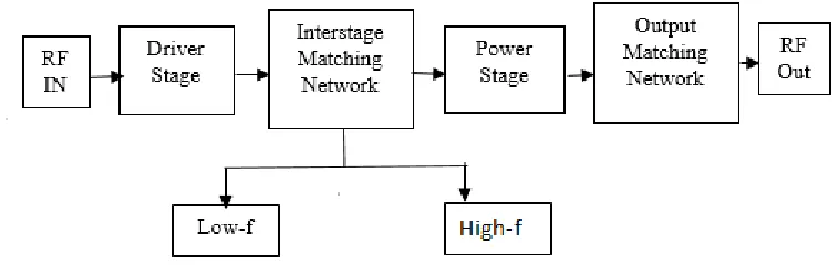
An amplifier is one of the most important electrical components in RF communication system. The schematic of a proposed two-stage broadband power amplifier with interstage network is shown in fig 1. The whole architecture is divided into four parts for simplification, as: 1) Driver Stage 2) Interstage Reconfigurable Network 3) Power Stage 4) Broadband Output Matching Network.
A cascaded topology is used in driver stage of power amplifier. Power stage is mainly responsible for power amplification. Size of transistor used in power stage is larger than as compared to as in driver stage transistor. A double-stacked FET structure is selected for both stages to overcome the low breakdown-voltage problem of CMOS FETs for both driver and power stage. Capacitors are connected at gate terminal to ensure that the voltage swing can be evenly distributed to each FET in the stack.
A reconfigurable interstage matching network is employed in this work to reconfigure the interstage matching according to the frequency of operation. For this, switch is used to reconfigure the interstage network. The interstage network is realized using high pass filter. The entire frequency range is divided into two sub-frequency bands, low from 0.65 to 0.85GHz and high from 0.85 to 1.20 GHz. The interstage matching component is reconfigured to provide the optimum matching for each sub-band based on the frequency of operation. In this way, a BW limitation has overcome. Output matching network is responsible for output return loss. Low-pass section is used in output matching network to optimize the impedance at 1GHz frequency which also helps to increase efficiency.
A. Power Amplifier design
L1 is connected at input side. It acts as input matching network to match output impedance. Driver amplifiers is used to boost the signal strength before power stage.
Fig. 1 Basic Block Diagram of Power Amplifier with Reconfigurable Interstage Network.
This system is designed for high power added efficiency PAE and high output power. PAE can be calculated as,
= (1)
Where, Pdc is dissipated power which is product of dissipated voltage and dissipated current in the circuit. It can be
calculated as,
= × (2)
B. Reconfigurable Network
Reconfigurable interstage network is designed to obtain optimized matching for each frequency band. Circuit schematic of reconfigurable network is shown in fig.3. The operation of reconfigurable network is based on frequency selection. It consists of high pass filter. It need to configure the components of high pass filter to optimize interstage impedance. Capacitor C1, C2, C3 and inductor L1 L2 forms high pass filter. L2. MOSFET M1, M2, M3, M4 are switch used to configure the components of network. Voltage controller A controls the value of capacitor C2 and inductor L1 and voltage controller B controls the value of capacitor C1 and inductor Switch A is ON for frequency band 0.65GHz to 0.85GHz where the matching components are optimized at 0.7GHz. And switch B is ON state for frequency band 0.85GHz to 1.20GHz for optimum performance at 1GHz.
C. Output Matching Network
Fig. 2 Circuit Diagram of double stacked Power Amplifier. Fig. 3 Circuit Diagram of Reconfigurable Network
Fig.4 Circuit Diagram of Output Matching Network.
IV.SIMULATION RESULTS
The system is designed to operate at frequency band from 0.65 – 2.45 GHz in ADS. Fig. 5 shows insertion loss of detail circuit of power amplifier with reconfigurable network. It is different for each frequency mode. Output power of PA is most important parameter which is shown in fig. 6. Power gain is calculated from Pout and Pin with reconfigurable and without reconfigurable network shown in fig. 7. This power amplifier shows maximum Power gain. Fig. 8 shows Pout versus gain response. PAE and adjacent channel power rejection is calculated at fig. 9.All the performance parameter of this work is shown in table1.
Fig. 7. Gain of power amplifier circuit Fig. 8 Output power Vs Gain response of power amplifier circuit
Fig.9 ACPR and PAE of power amplifier.
Table1. Obtained Performance parameter from simulations in ADS at 0.85 frequency
Sr. No. Parameters Obtained Values
1 Output Power (W) 28.123 dBm
2 1 dB Drain Efficiency (%) 58.065
3 Gain (dB) 43.77
4 Bandwidth (MHz) 550
5 Supply Voltage (V) 5
6 Current (mA) 194
V. CONCLUSION AND FUTURE WORK
In this work, a broadband two-stage SOI CMOS stacked-FET PA with a reconfigurable interstage matching network has been developed. Output matching is realized using a low-pass network.
REFERENCES
1. J. Kim, H. Son, W. Kim, and C. Park, “Single-ended CMOS doherty power amplifier using current boosting technique,” IEEE Microw. Wireless Compon. Lett.,vol 24, no. 5,app. 342-344, May 2014
2. R. Wu, J. Lopez, Yan Li, and D. Y. C. Lie,” A highly efficient 1-watt broadband class-J SiGe power amplifier at 700 MHz,” in Proc. 12th Top. Silicon Monolithic Integr. Circuit RF Syst. Meeting, 2012, pp.69-72.
3. J. Woo, S. Park, U. Kim, and Y. Kwon, “Dynamic stack-controlled CMOS RF power amplifier for wideband envelope tracking,” IEEE Trans. Microw. Theory Techn., vol. 62, no. 12, pp. 3452–3464, Dec 2014.
4. R. Zhang, M. Acar, M. P. Heijden, M. Apostolidou, L. C. N. Vreede, and D. M. W. Leenaerts,” A 550-1050 MHz +30dBm class-E power amplifier in 65nm CMOS,” in Proc. IEEE RF Integr. Circuits Symp. Dig., Jun 2014, pp. 1-4.
5. S. Park, J. Woo, U. Kim, Y. Kwon, “Broadband CMOS Stacked Power Amplifier Using Reconfigurable Interstage Network for Wideband Envelope Tracking application.” in Proc IEEE Trans. RF Integr. Circuit, Symp. Dig, Jun 2014, pp.145-148.
6. R. Wu, Y.T. Liu, J. Lopez, Member, C. Schecht, Y. Li, D. Y. C. Lie,” High-efficiency silicon-based envelope -tracking power amplifier design with envelope shaping for wideband wireless application,” IEEE J. Solid-State Circuits, vol.48, no. 9, pp 2030-3040, Sep. 2013. 7. Q. H. Duong and S. G. Lee, "86 dB 1.4mW 1.8V 0.07mm2 single-stage variable gain amplifier in 0.18 μm CMOS," Electron. Lett.,vol.
43, pp. 19-20, 2007.
8. Yi-Keng Hsieh et al. “A 60-Ghz Broadband Low-Noise Amplifier with Variable-Gain Control in 65 n m nm CMOS ”, IEEE Microwave And wireless components letters, Vol-21, No-11, Nov 2011.
9. D Kang, B. Park, D. Kim, J. Kim, Y. Cho , and B. Kim, “Envelope-tracking CMOS power amplifier module for LTE application,” IEEE Trans. Microw. Theory Techn.,vol 61, no. 10, app 3763-3773, Oct.2013.
BIOGRAPHY
Neha Kashiwaris a M.E. student in SKNCOE, Vadgaon, Pune, India, pursuing Master of Engineering degree under the