HAN, KIJEONG. Design, Analysis, and Optimization of 1.2 kV 4H-SiC Planar-Gate Power MOSFETs for Improved High Frequency Switching. (Under the direction of Dr. B. Jayant Baliga).
This research focuses on the analysis, design, fabrication, and testing of high frequency 1.2
kV 4H-SiC Planar-Gate Power MOSFETs. To achieve the high switching capability, the
MOSFET’s reverse transfer capacitance (Cgd) and gate-to-drain charge (Qgd), resulting from the
gate-to-drain overlap above the JFET region, must be minimized because they are the dominant
components limiting the switching speed. Therefore, achieving low values for the High-Frequency
Figures-of-Merit (HF-FOMs), defined as [Ron×Cgd] and [Ron×Qgd], is a main goal for this research.
Gate oxide thickness (tOX) of 50 nm and channel length (LCH) of 0.5 µm were fixed for all the 1.2
kV 4H-SiC Planar-Gate Power MOSFET structures throughout this thesis.
An extensive study of structure optimizations for conventional 1.2 kV 4H-SiC Planar-Gate
Power MOSFETs to reduce on-resistance and improve the switching capability has been carried
out first with analytical models and numerical simulations.
In order to improve the HF-FOM, a 1.2 kV 4H-SiC Split-Gate MOSFET (SG-MOSFET)
structure was experimentally verified for the first time. Compared with the conventional
Planar-Gate MOSFET, the SG-MOSFET has 2.4× smaller HF-FOM [Ron×Qgd] due to the reduced
gate-to-drain charge.
To further improve the device electrical characteristics, a novel 1.2 kV 4H-SiC
Buffered-Gate MOSFET (BG-MOSFET) structure has been experimentally demonstrated to have superior
HF-FOMs for the first time. The split-gate electrode is buffered from the drain by extending the
P+ shielding region beyond its edge. From the measured data on devices fabricated in a 6-inch
Planar-Gate MOSFET and Split-Gate MOSFET, respectively.
Most SiC planar-gate power MOSFETs have been reported with the linear cell topology. To
understand the electrical performance with various channel and JFET densities in the MOSFET
structures, different cell topologies have been studied. A 1.2 kV rated 4H-SiC MOSFET with
octagonal-cell topology has been experimentally demonstrated for the first time. From the measured
electrical characteristics, the MOSFET with the octagonal-cell topology is demonstrated to have
1.4× superior HF-FOM [Ron×Qgd], and 2.1× superior HF-FOM [Ron×Cgd] compared with the
conventional linear-cell MOSFET. Moreover, the Split-Gate (SG) concept is combined with the
octagonal cell topology for the first time (SG-OCTFET) to achieve a further improvement in Cgd,
Qgd, and HF-FOMs. A detailed comparison of the measured electrical characteristics for the 1.2
kV 4H-SiC power MOSFETs with linear, square, hexagonal, octagonal, and Split-Gate octagonal
cell topologies fabricated at X-Fab using the same design rules and process flow as the
conventional linear-cell MOSFETs will be provided.
© Copyright 2019 by Kijeong Han
for Improved High Frequency Switching.
by Kijeong Han
A dissertation submitted to the Graduate Faculty of North Carolina State University
in partial fulfillment of the requirements for the degree of
Doctor of Philosophy
Electrical Engineering
Raleigh, North Carolina
2019
APPROVED BY:
_______________________________ _______________________________ Dr. B. Jayant Baliga Dr. Victor Veliadis
Chair of Advisory Committee
ii DEDICATION
iii BIOGRAPHY
Kijeong Han received the B.S. and M.S. degrees in electrical engineering at Korea Aerospace
University, Goyang, South Korea in 2012, and Korea Advanced Institute of Science and
Technology (KAIST), Daejeon, South Korea in 2014, respectively. He started working in 2015
toward the Ph.D. degree in wide bandgap high voltage and high power devices in the department
of Electrical and Computer Engineering at North Carolina State University. He has worked for the
U.S. Department of Energy (DOE) funded PowerAmerica project to design novel 4H-SiC power
MOSFETs. In the project, he contributed to establishing the PRocess Engineered for
manufacturing Silicone Carbide (SiC) Electronic-devices (PRESiCETM) at a foundry company,
X-Fab, Texas. In addition, he has performed device designs for the Solar Energy Technologies Office
(SETO) project supported by the U.S. DOE to achieve PV inverter systems using bi-directional
FETs (BiDFETs). His research interests include the design, fabrication, characterization, and
analysis of high power devices. He has authored and coauthored over 20 technical journal and
conference papers. He received the Early Doctoral Research Achievement Award from College of
iv ACKNOWLEDGMENTS
I would like to thank my advisor, Dr. B. J. Baliga, for his guidance, strong support, and
encouragement over my entire graduate study and research at North Carolina State University. His
wide knowledge, brilliant ideas, creative thinking, and great insights have been a source of my
inspiration. All the significant outcomes I could achieve during my graduate study are thanks to
his devotion and helps. It has been an invaluable experience to be one of his graduate students, not
only for learning the research works, but also for studying under his passionate and diligent
attitude.
I would like to thank Dr. Victor Veliadis of the Power America institute. His support in the
Power America projects to fabricate all the SiC devices at 6-inch foundry, X-Fab helps me to
achieve all the novel device structures and complete this work successfully.
I am also appreciative to have Dr. Subhashish Bhattacharya and Dr. Ramon Collazo as my
doctoral committee members. Their expertise, encouragement, and feedback have enriched my
graduate study.
It has been a great pleasure to work with the excellent staffs and students at North Carolina
State University. I appreciate Dr. Ginger Yu, Dr. Woongje Sung, Mr. Ajit Kanale, Ms. Aditi
Agarwal, Mr. Jeffrey Harmon, Mr. Adam Morgan, Mr. Bahji Ballard, Mr. Anup Anurag, Mr.
Tzu-Hsuan Cheng, Dr. Douglas C. Hopkins, Dr. WoongSun Kim, Dr. Q. Jon Zhang, Mr. Austin Tucker,
Mr. Saimum Syed, Mr. Chris Lach, Mr. Runxue Liao, Mr. Antuwon Butler, Mr. Cristian Melara,
and Mr. Caelin Lewis for considerable assistances and constructive discussions.
Lastly, I would like to thank my family for being supportive and dedicated to my entire
academic career and personal life all the time. Special thanks to my wife for her love, patience,
v TABLE OF CONTENTS
LIST OF TABLES ... vii
LIST OF FIGURES ... viii
Chapter 1: Introduction ... 1
1. Background & Motivation ... 1
2. Switching Characteristics ... 3
3. PRESiCETM ... 4
4. Outline of Dissertation ... 6
Chapter 2: Optimization of 1.2 kV 4H-SiC Linear Cell Planar-Gate MOSFETs ... 11
1. Background & Motivation ... 11
1.1. Major Issues of 4H-SiC MOSFETs ... 11
1.2. Inversion vs. Accumulation Channels ... 13
2. Structure Optimization ... 15
2.1. JFET Region Optimization ... 16
2.2. Analysis with Analytical Models ... 18
2.3. TCAD Numerical Simulations ... 22
3. Fabrication of 1.2 kV 4H-SiC Planar-Gate MOSFETs ... 24
3.1. Structure Information ... 24
3.2. Hybrid-JTE Edge Termination ... 26
3.3. Layout Description... 27
3.4. Process Flow ... 28
4. Experimental Results and Discussions ... 30
4.1. Experimental Results ... 30
4.2. Discussions ... 38
5. Conclusions ... 41
Chapter 3: Demonstration of 1.2 kV 4H-SiC Linear Cell Split-Gate MOSFETs (SG-MOSFET) with Superior Electrical Characteristics ... 46
1. Background & Motivation ... 46
2. Structure Optimization using TCAD Numerical Simulations ... 47
2.1. SiC Split-Gate vs. Terraced-Gate MOSFETs ... 47
2.2. Structure Optimization ... 50
3. Fabrication of 1.2 kV 4H-SiC SG-MOSFETs ... 53
3.1. Layout Description... 53
3.2. Process Flow ... 54
4. Experimental Results and Discussions ... 56
4.1. Experimental Results ... 56
4.2. Discussions ... 69
5. Conclusions ... 70
Chapter 4: Development of Novel 1.2 kV 4H-SiC Linear Cell Buffered-Gate MOSFETs (BG-MOSFET) for Extremely Low HF-FOMs ... 76
1. Background & Motivation ... 76
vi
2.1. N+ JFET Doping Concentration ... 78
2.2. Structure Optimization ... 81
3. Fabrication of 1.2 kV 4H-SiC BG-MOSFETs ... 85
3.1. Layout Description... 85
3.2. Process Flow ... 86
4. Experimental Results and Discussions ... 87
4.1. Experimental Results ... 87
4.2. Discussions ... 93
5. Conclusions ... 95
Chapter 5: Analysis for Various Cell Topologies of 1.2 kV 4H-SiC Planar-Gate MOSFETs and JBSFETs ... 99
1. Background & Motivation ... 99
1.1. Cell Topologies ... 100
1.2. Monolithically Integrated JBS Diode and MOSFET (JBSFET)... 101
2. Structure Optimization using TCAD Numerical Simulations ... 104
2.1. Square & Hexagonal Cell Optimization ... 104
2.2. Octagonal Cell Optimization ... 105
2.3. Split-Gate Octagonal Cell Optimization ... 107
2.4. Electric Field Distribution at Schottky Contact in Various Cell JBSFETs . 108 3. Fabrication of 4H-SiC MOSFETs and JBSFETs with Various Cell Topologies ... 111
3.1. Layout Description... 111
3.2. Process Flow ... 113
4. Experimental Results and Discussions ... 115
4.1. Experimental Results for MOSFETs with Various Cell Topologies ... 115
4.2. Experimental Results for Split-Gate Octagonal MOSFETs (SG-OCTFET) 124 4.3. Experimental Results for JBSFETs with Various Cell Topologies ... 126
4.4. Discussions ... 132
5. Conclusions ... 138
Chapter 6: Summary and Future Work ... 144
1. Major Accomplishment ... 144
2. Future Work ... 146
Appendix: Comprehensive Physics of Third Quadrant Characteristics for Accumulation- and Inversion-Channel 1.2 kV 4H-SiC MOSFETs ... 149
1. Introduction ... 149
2. Device Structure and Fabrication Technology ... 150
3. Experimental Results and Analysis ... 151
vii LIST OF TABLES
Table 2.1 Design variations of JFET widths and doping concentrations... 25
Table 2.2 Experimental results for 1.2 kV Acc MOSFET structures with and without the enhanced NJFET ... 39
Table 2.3 Experimental results for 1.2 kV Acc and Inv MOSFET structures with the enhanced NJFET ... 40
Table 3.1 Experimental results for 1.2 kV Acc- and Inv-channel SG-MOSFETs ... 70
Table 4.1 Structural parameters of 1.2 kV C-, SG-, and BG-MOSFETs for fabrication ... 84
Table 4.2 Experimental results for 1.2 kV Acc- and Inv-channel BG-MOSFETs ... 94
Table 5.1 Fabricated 1.2 kV 4H-SiC various cell MOSFETs with structural parameters .... 112
Table 5.2 Fabricated 1.2 kV 4H-SiC various cell JBSFETs with structural parameters ... 112
Table 5.3 Experimental results for 1.2 kV 4H-SiC Acc octagonal cell MOSFETs compared with conventional linear MOSFET ... 133
Table 5.4 Experimental results for 1.2 kV 4H-SiC MOSFETs with various cell topologies ... 135
viii LIST OF FIGURES
Figure 1.1 (a) Thermal resistance used in the package of 1.2 kV SiC MOSFETs and Silicon IGBTs as a function of chip size, (b) Calculated maximum frequency of 1.2 kV SiC MOSFETs and IGBTs with available electrical characteristics from the datasheets, using duty cycle of 0.5 ... 2
Figure 1.2 (a) Clamped inductive load switching circuit configuration with a free-wheeling diode (high side) and 4H-SiC MOSFET (low side), (b) Turn-on switching waveforms for gate voltage (Vg), drain current (Id), and drain
voltage (Vd) of the switching circuit ... 3
Figure 1.3 (a) Fabricated power devices on a 4H-SiC 6-inch wafer, (b) Semi-automatic
Signatone probe station and Keysight B1505A curve tracer ... 5
Figure 1.4 Wafer map and statistical distribution of the on-resistance of power
MOSFETs manufactured using PRESiCETM technology ... 5
Figure 1.5 Wafer map and statistical distribution of the threshold voltage for power
MOSFETs manufactured using PRESiCETM technology ... 6
Figure 2.1 Half-cell cross-sectional view of the 4H-SiC MOSFET structure... 12
Figure 2.2 Cross-sectional views of the (a) Inversion-mode channel MOSFET (InvFET), (b) Accumulation-mode channel MOSFET (AccFET) ... 13
Figure 2.3 (a) Field effect channel mobilities of SiC AccFETs and InvFETs at high
temperatures, (b) Trade-off between channel mobility and threshold voltages... 14
Figure 2.4 Electrostatic potential simulation results along with X dimension for (a) Acc and (b) Inv MOSFETs with the channel length of 0.3µm at Vd=1200V and
Vg=0V. The channel barriers are shown in the figure ... 15
Figure 2.5 (a) Cross section view of the SiC MOSFETs with detailed structural information, and (b) simulation results with various structural parameters
conducted by A. Saha and J. A. Cooper ... 15
Figure 2.6 Unit cell cross sectional view of the 4H-SiC MOSFET with series resistance
components and reverse transfer capacitance (Cgd) ... 17
Figure 2.7 Cross sectional view of the 1.2 kV-rated 4H-SiC MOSFET with detailed
structural parameter information... 18
Figure 2.8 Analytically calculated Ron,sp with Rch,sp, Rdrift,sp, and RJFET,sp for the
conventional MOSFETs having various WJFET and NJFET of (a) 8×1015 cm-3
ix Figure 2.9 Measured channel mobilities (µCH,FE) for Acc and Inv MOSFETs and
analytically calculated drift region mobilities (µDrift) at high temperatures ... 20
Figure 2.10 Comparison of Rch, Rjfet, and Rdrift components using analytical models for
Acc and Inv MOSFETs with various JFET widths at (a) 25°C and (b) 150°C. The contribution of Rjfet and Rdrift to Ron becomes larger than Rch at narrower
JFET width. The impact is greater in the Acc structures ... 21
Figure 2.11 Analytically calculated increase in the ratio [Ron(150oC)/Ron(25oC)] for Acc
and Inv MOSFETs with various JFET widths. The ratio is bigger when the
JFET width becomes smaller ... 22
Figure 2.12 (a) Breakdown Voltage (BV) simulation results with various NJFET and WJFET
with the oxide field limitation of 4 MV/cm, (b) The oxide electric field simulations with the enhanced JFET doping of 3×1016 cm-3 at V
d of 1600 V ... 23
Figure 2.13 TCAD simulation results for (a) Ron,sp, and (b) Qgd,sp, Cgd,sp, and HF-FOMs
with various WJFET. The optimum WJFET is determined to be 0.7 µm ... 23
Figure 2.14 Designed implant profiles for Acc- and Inv-channel, and enhanced JFET.
Series implants of Aluminum and Nitrogen were used, respectively ... 25
Figure 2.15 Cross-sectional view of the Hybrid-JTE edge termination. The termination
consists of RA-JTE and MFZ-JTE to achieve reliable breakdown voltage ... 26
Figure 2.16 TCAD numerical simulations for breakdown voltages with the Hybrid-JTE
and the SZ-JTE ... 27
Figure 2.17 PowerAmerica (PA) Budget Period 2 (BP2) 1st lot layout for the 1.2 kV
conventional planar power MOSFET structures... 28
Figure 2.18 Fabrication process flow for the Acc 1.2 kV 4H-SiC conventional planar-gate MOSFETs ... 29
Figure 2.19 SEM cross-sectional image for the fabricated 1.2 kV SiC Acc-channel
planar-gate power MOSFET with WJFET of 0.7 µm ... 30
Figure 2.20 Typical output characteristics for Acc MOSFET_J_0.7 and MOSFET_1.1
measured at Vg from 0 to 25 V with 5 V steps at room temperature ... 31
Figure 2.21 Wafermaps of Ron,sp for Acc MOSFET_J_0.7 and MOSFET_1.1 extracted at
Vg of 20 V and Id of 10 A from 60 devices each ... 31
Figure 2.22 Typical transfer characteristics for Acc MOSFET_J_0.7 and MOSFET_1.1
x Figure 2.23 Wafermaps of Vth for Acc MOSFET_J_0.7 and MOSFET_1.1 extracted at Vd
of 0.1 V and Id of 1 mA from 60 devices each ... 33
Figure 2.24 Typical reverse transfer capacitance (Cgd) for Acc MOSFET_J_0.7 and
MOSFET_1.1 measured at room temperature ... 34
Figure 2.25 Wafermaps of Cgd for Acc MOSFET_J_0.7 [10] and MOSFET_1.1 extracted
at Vd of 1000 V from 60 devices each ... 34
Figure 2.26 Typical measured gate-to-drain charge (Qgd) for Acc MOSFET_J_0.7 and
MOSFET_1.1 at Vd of 800 V and Id of 10 A at room temperature ... 35
Figure 2.27 Comparison of blocking capability. MOSFETs with narrower JFET widths
(MOSFET_J_0.7) show lower leakage currents ... 36
Figure 2.28 Cumulative distribution of leakage current measured from total 60 dies on a
6-inch wafer at Vd=1000 V, Vg=0 V at room and high temperature (175°C) ... 36
Figure 2.29 Normalized Ron from measured output characteristics of the fabricated Acc
and Inv-channel SiC MOSFETs with different JFET widths (0.7, 1.1, 1.5
µm) ... 37
Figure 3.1 Cross sectional views of (a) experimentally demonstrated Si Split-Gate MOSFET, (b) Si Terraced-Gate MOSFET, and (c) simulated SiC Split-Gate
MOSFET ... 47
Figure 3.2 Cross-sectional view of simulated 1.2 kV SiC Acc-channel conventional MOSFET (left), Split-Gate MOSFET (center), and Terraced-Gate MOSFETs with detailed simulation structural parameters ... 48
Figure 3.3 Simulation results of electric field distribution at Vd of 1200 V for
SG-MOSFET (left) and TG-SG-MOSFET (right) with X of 0.5 µm ... 48 Figure 3.4 (a) Simulation results of electric field distribution at Vd of 1200 V for
SG-MOSFET with X of 0.1 µm (left) and 0.7 µm (right). (b) Simulated oxide electric field at Vd=1200 V as a function of X width in SG-MOSFET (Black
line) and TG-MOSFET (Red line) structures ... 49
Figure 3.5 Simulation results of Qgd,sp and HF-FOM (Ron×Qgd) as a function of X length
for SG-MOSFETs and TG-MOSFETs ... 49
Figure 3.6 Cross-sectional view of the 1.2 kV SiC conventional MOSFET (left) and SG-MOSFET (center) structures. Structural parameters are given ... 50
Figure 3.7 Simulation results of Ron,sp as a function of WJFET in both Acc- and
xi Figure 3.8 Simulated (a) Ron,sp, Qgd,sp, Cgd,sp, (b) Oxide electric field, HF-FOM
(Ron×Qgd), and HF-FOM (Ron×Cgd) as a function of X width in Acc-channel
SG-MOSFETs with fixed WJFET of 0.9 µm ... 52
Figure 3.9 Simulated Ron,sp, Cgd,sp, and HF-FOM (Ron×Cgd) as a function of Temperature
in both Acc- and Inv-channel SG-MOSFET structures ... 53
Figure 3.10 PowerAmerica (PA) Budget Period 2 (BP2) (a) 1st lot and (b) 2nd lot layouts
for the 1.2 kV Split-Gate power MOSFET structure ... 54
Figure 3.11 Fabrication process flow for the 1.2 kV 4H-SiC Split-Gate MOSFETs... 55
Figure 3.12 SEM cross-sectional image for the fabricated 1.2 kV SiC Inv-channel
Split-Gate power MOSFET with WJFET of 0.7 µm ... 56
Figure 3.13 Typical output characteristics for Acc conventional MOSFET and
SG-MOSFET measured at Vg from 0 to 25 V with 5 V steps at room temperature ... 57
Figure 3.14 Typical transfer characteristics for Acc conventional MOSFET and
SG-MOSFET measured at Vd of 0.1 V at room temperature ... 58
Figure 3.15 Comparison of blocking capability for Acc conventional MOSFET and
SG-MOSFET ... 58
Figure 3.16 Typical reverse transfer capacitance (Cgd) for Acc conventional MOSFET
and SG-MOSFET measured at room temperature ... 59
Figure 3.17 Typical measured gate-to-drain charge (Qgd) for Acc conventional MOSFET
and SG-MOSFET measured at Vd of 800 V and Id of 10 A at room
temperature ... 60
Figure 3.18 Typical output characteristics for Acc-channel SG-MOSFET measured at Vg
from 0 to 25 V with 5 V steps at room and high (150°C) temperature ... 61 Figure 3.19 Typical output characteristics for Inv-channel SG-MOSFET measured at Vg
from 0 to 25 V with 5 V steps at room and high (150°C) temperature ... 61 Figure 3.20 Normalized on-resistance (Ron) for fabricated Acc-, Inv-channel
SG-MOSFETs, and conventional MOSFET from a Wolfspeed datasheet ... 62
Figure 3.21 Transfer characteristics for fabricated Acc- and Inv-channel SG-MOSFETs measured from 25°C to 150°C with 25°C step. Threshold voltages (Vth) are
xii Figure 3.22 Threshold voltages (Vth) were experimentally extracted, and analytically
calculated for fabricated Acc- and Inv-channel SG-MOSFETs at
temperatures up to 150°C ... 64
Figure 3.23 Measured C-V curves at low (1 kHz) and high (100 kHz) frequencies for
fabricated Acc- and Inv-channel MOS structures ... 65
Figure 3.24 Extracted Dit for fabricated Acc- and Inv-channel MOS structures using the
High-Low method. Both structures show similar Dit ... 65
Figure 3.25 Typical blocking characteristics of fabricated Acc- and Inv-channel
SG-MOSFETs measured at room temperature ... 66
Figure 3.26 Measured leakage currents at Vd of 1000 V for fabricated Acc- and
Inv-channel SG-MOSFETs at elevated temperatures ... 67
Figure 3.27 Reverse transfer capacitance (Cgd) of fabricated Acc- and Inv-channel
SG-MOSFETs measured at elevated temperatures ... 67
Figure 3.28 Measured gate charge of Acc- and Inv-channel SG-MOSFETs at Vd=800 V
and Id=10 A. Both structures have the similar Qgd values despite the plateau
at higher gate voltage for the Inv device ... 68
Figure 4.1 (a) Schematic cross-section of a unit cell of the 1.2 kV SiC Central implant (CI) MOSFET, (b) Numerical simulations comparing the electrical field on the gate oxide at Vd=960 V with commercial conventional MOSFET
(C2M0080120D) ... 76
Figure 4.2 Cross-sectional views of 4H-SiC 1.2 kV conventional (C), Split-Gate (SG), and Buffered-Gate (BG) MOSFETs. All structures have the same channel
length (0.5 µm) and WJFET (0.7 µm) ... 78
Figure 4.3 Simulation results for optimization of the N+ JFET doping concentration in Acc and Inv BG-MOSFETs to minimize the Oxide electric field and
on-resistance. Optimum value is 3×1017 cm-3 ... 79 Figure 4.4 Forward conduction simulation results at Vg=20 V and Id=10 A. Current
density is shown in the cross-section of Inv-channel BG-MOSFET structures with N+ JFET doping of (a) 1×10¹⁷, (b) 2×10¹⁷, and (c) 4×1017 cm-3,
respectively ... 80
Figure 4.5 Simulation results of (a) Qgd,sp, Cgd,sp, and Ron,sp, (b) Oxide electric field,
HF-FOM [Ron×Qgd], and HF-FOM [Ron×Cgd] as a function of X1 width for
BG-MOSFETs. The solid and dashed lines are for the higher (3×1017 cm-3) and
xiii Figure 4.6 Simulation results of (a) Qgd,sp, Cgd,sp, and Ron,sp, (b) Oxide electric field,
HF-FOM [Ron×Qgd], and HF-FOM [Ron×Cgd] as a function of X2 width for
BG-MOSFETs. The solid and dashed lines are for the higher (3×1017 cm-3) and
lower (1.5×1017 cm-3) N+ JFET doping concentration, respectively ... 83
Figure 4.7 PowerAmerica (PA) Budget Period 2 (BP2) 2nd lot layouts for the 1.2 kV
Buffered-Gate power MOSFET structures ... 85
Figure 4.8 Fabrication process flow for the 1.2 kV 4H-SiC Buffered-Gate MOSFETs ... 87
Figure 4.9 SEM image for the fabricated Acc BG-MOSFET. It is clearly seen that the
split poly-Si gates are buffered by the P+ shielding regions ... 88
Figure 4.10 Typical measured output characteristics of fabricated 1.2 kV rated Acc and Inv BG-MOSFETs with high or low N+ JFET doping measured at Vg from 0
to 25 V with 5 V steps... 89
Figure 4.11 (a) Cross-section view of the BG-MOSFET, (b) N+ JFET implant profiles along with “a” and “b” marked in (a). Higher N+ JFET doping is required to
compensate the P-base in Inv BG-MOSFET, resulting in the reduced BV ... 89
Figure 4.12 Typical room temperature blocking characteristics (Vgs = 0 V) of fabricated
SiC Acc- and Inv -channel BG-MOSFETs with high or low N+ JFET doping.
BV is defined at Id = 100 µA. ... 90
Figure 4.13 Measured transfer characteristics for fabricated SiC Acc C-, Acc SG-, Acc and Inv BG-MOSFETs with high or low N+ JFET doping measured at Vd of
0.1 V. Vth was extracted at Id=1 mA ... 91
Figure 4.14 Typical measured reverse transfer capacitance of fabricated SiC C-, SG-, and BG-MOSFETs. The Acc BG-MOS_H and _L have much smaller Cgd ... 92
Figure 4.15 Measured gate charge at Vd=800 V and Id=10 A of fabricated SiC Acc C-,
SG-, and BG-MOSFETs with high or low N+ JFET doping. Much smaller
plateau (Qgd) is observed in the Acc BG-MOS_H and _L... 92
Figure 5.1 (a) Various cell topologies for planar-gate power MOSFETs, (b) Schematic
view of the octagonal cell topology ... 101
Figure 5.2 (a) A JBSFET device symbol: Monolithic integration of JBS diode in a SiC MOSFET structure, (b) Cross-sectional view of the JBSFET. Schottky area is integrated in the MOSFET unit cell structure ... 102
xiv (c) Square, (d) Hexagonal, (e) Octagonal, (f) Split-Gate Octagonal. All the
structures have the same channel length of 0.5 µm ... 103
Figure 5.4 Simulation results of (a) Qgd,sp, Cgd,sp, and Ron,sp, (b) HF-FOM [Ron×Qgd],
HF-FOM[Ron×Cgd], and oxide electric field (at Vd=1200 V and Vg=0 V) as a
function of WJFET for the Acc square and hexagonal cell topology ... 105
Figure 5.5 Simulation results of (a) Qgd,sp, Cgd,sp, and Ron,sp, (b) HF-FOM [Ron×Qgd],
HF-FOM [Ron×Cgd], and oxide electric field (at Vd=1200 V and Vg=0 V) as a
function of WJFET in the Acc octagonal cell topology ... 106
Figure 5.6 Simulation results of (a) Qgd,sp, Cgd,sp, and Ron,sp, (b) HF-FOM [Ron×Qgd],
HF-FOM [Ron×Cgd], and oxide electric field (at Vd=1200 V and Vg=0 V) as a
function of “X” in the SG-OCTFET structure ... 108
Figure 5.7 Cell topologies for the fabricated 1.2 kV 4H-SiC JBSFETs: (a) Linear, (b) Hexagonal, (c) Octagonal, and (d) JBSFET cell cross-section at A-A’ for all
the cell topologies ... 109
Figure 5.8 (a) TCAD simulation structure for linear and cylindrical (rotated at the right edge) JBS diodes that are monolithically integrated in JBSFETs. (b)
Simulation results of electric field distribution at 1.2 kV for linear cell (left) and cylindrical cell JBS diodes (right). (c) Extracted electric field values at
1.2 kV along with the lines marked in red in (b) ... 110
Figure 5.9 PowerAmerica (PA) Budget Period 3 (BP3) 1st lot layouts for the 1.2 kV
power MOSFETs and JBSFETs with various cell topologies ... 113
Figure 5.10 Fabrication process flow for the 1.2 kV 4H-SiC planar-gate power JBSFETs .... 114
Figure 5.11 Typical measured output characteristics at Vg=20 V of fabricated linear cell
and octagonal cells with different WJFET (O_J# or O_J#_C for the compact
design). The Oct MOSFETs with wider WJFET show lower Ron values. The
compact design has a lower Ron for the same WJFET=1.1 µm ... 116
Figure 5.12 Measured reverse transfer capacitance (Cgd) of fabricated linear cell and
octagonal cells with different WJFET. The Oct MOSFETs with narrower
WJFET have lower Cgd values as expected ... 116
Figure 5.13 Measured gate charge of fabricated linear cell and octagonal cells with different WJFET at Vd=800 V and Id=10 A. The plateaus (Qgd) get gradually
smaller with narrower WJFET in Oct MOSFETs ... 117
Figure 5.14 Typical measured output characteristics at Vg=20V of fabricated (a)
xv Figure 5.15 Measured transfer characteristics for fabricated Acc and Inv MOSFETs with
various cell topologies. Vth was extracted at Id=1 mA ... 118
Figure 5.16 Typical blocking characteristics (Vg=0 V) of fabricated (a) Acc and (b) Inv
MOSFETs. BV is defined at Id=100 µA. Smaller BV is observed in Sqr and
Hex MOSFETs with WJFET of 1.1 µm compared with the others ... 119
Figure 5.17 (a) Electrostatic potential simulation results along with X dimension for both Acc and Inv linear MOSFETs with the channel length of 0.5 µm at Vd=1200
V and Vg=0 V. The channel barrier for the Acc and Inv structures is shown in
the figure. (b) The extracted channel barrier from the simulations as a
function of the channel length for both the Acc and Inv linear MOSFETs ... 120
Figure 5.18 Typical measured reverse transfer capacitance (Crss) of fabricated (a) Acc and
(b) Inv MOSFETs with various cell topologies. The Oct cell MOSFETs show lower Crss values than the others ... 121
Figure 5.19 Measured input capacitance (Ciss) of fabricated (a) Acc and (b) Inv
MOSFETs. The Sqr and Hex MOSFETs with WJFET of 1.1 µm show the
smallest Ciss values at Vd=1 kV, but the highest values at low Vd ... 122
Figure 5.20 Typical measured output capacitance (Coss) of fabricated Acc and Inv
MOSFETs with various cell topologies. All the structures have similar Coss
regardless of the channel types and cell topologies ... 122
Figure 5.21 Measured gate charge at Vd=800 V and Id=10 A of fabricated (a) Acc and (b)
Inv MOSFETs. A large gate plateau (Qgd) is observed in the Sqr and Hex
designs. Much smaller gate plateau (Qgd) is observed in the Oct designs ... 123
Figure 5.22 Typical measured output characteristics at Vg=20 V of fabricated octagonal
cell topologies and SG-OCTFET (O_J1.5_SG). The active area is 0.045 cm2 .... 124
Figure 5.23 Typical measured blocking characteristics for fabricated octagonal cell
topologies and SG-OCTFET (O_J1.5_SG) ... 125
Figure 5.24 Measured reverse transfer capacitance (Cgd) of fabricated octagonal cell
topologies and SG-OCTFET (O_J1.5_SG) ... 125
Figure 5.25 Measured gate charge of fabricated octagonal cell topologies and
SG-OCTFET (O_J1.5_SG) at Vd=800 V and Id=10 A ... 126
Figure 5.26 Typical measured output characteristics at Vg=20 V of fabricated 1.2 kV Acc
JBSFETs with various cell topologies. Active area is 0.045 cm2 ... 127
Figure 5.27 Measured transfer characteristics for fabricated Acc JBSFETs with various
xvi Figure 5.28 Typical room temperature blocking characteristics (Vgs = 0 V) of fabricated
JBSFETs. BV is defined at Id = 100 µA ... 128
Figure 5.29 Measured 3rd quadrant characteristics of fabricated Acc JBSFETs with
various cell topologies ... 129
Figure 5.30 Typical measured reverse transfer capacitance of fabricated JBSFETs with various cell topologies. The Hex cell has higher Crss values while the Oct cell
has lower Crss values than the Linear design ... 129
Figure 5.31 Measured input capacitance (Ciss) of fabricated JBSFETs. The Hexagonal
JBSFET show smaller Ciss value at Vd=1 kV, but the highest value at low Vd
as shown in the inset zoom-in graph ... 130
Figure 5.32 Typical measured output capacitance (Coss) of fabricated JBSFETs with
various cell topologies. All the structures have similar Coss values regardless
of the cell topologies ... 131
Figure 5.33 Measured gate charge at Vd=800 V and Id=10 A of fabricated JBSFETs. A
large gate plateau (Qgd) is observed in the Hex design. Much smaller gate
plateau (Qgd) is observed in the Oct design ... 132
Figure A.1 Cross-sectional view of fabricated 1.2 kV SiC accumulation (Acc)- and
inversion (Inv)-channel MOSFETs. The gate oxide thickness is 55 nm ... 151
Figure A.2 Measured 3rd quadrant I-V characteristics for (a) Acc and (b) Inv MOSFETs
with LCH=0.5 µm at room temperature ... 152
Figure A.3 Simulated electrostatic potential at near oxide gate interface ... 152
Figure A.4 Cross-sections of simulated total current density for Acc (left) and Inv (right) MOSFETs at various drain voltages: a. 0; b. -1.2; c. -1.9; d. -2.8; e. -5.0 V ... 153
Figure A.5 (a) Simulation results of 3rd quadrant I-V characteristics for Acc-channel MOSFETs (LCH=0.5 µm), (b) zoomed-in body diode current (Ih) results from
(a), and (c) cross-sections of simulated electron current density ... 155
Figure A.6 (a) A schematic view of orthogonal P+ contact, (b) Simulation results for
Acc MOSFETs (LCH=0.5 µm) with RP+ (=RC + RInt) of 0.16 and 1.6 Ω ... 156
Figure A.7 Measured 3rd quadrant I-V characteristics for (a) Acc and (b) Inv MOSFETs
with various LCH at room temperature (solid) and 150°C (dashed) ... 157
Figure A.8 Simulation results for (a) Acc and (b) Inv MOSFETs with various LCH at
xvii Figure A.9 Measured 3rd quadrant I-V characteristics for (a) Acc and (b) Inv MOSFETs
with LCH=0.5 µm at various Vg from -4 to 4 V at room temperature ... 158
Figure A.10 (a) Simulation results of 3rd quadrant total and hole (inset) current for Acc
MOSFETs (LCH=0.5 µm) at Vg from -4 to 4 V at room temperature.
Simulated electrostatic potential at (b) Vd=0 V and Vg from -4 to 4 V, and at
(c) various Vd (i. 0; ii. -1.2; iii. -2.1; iv. -3; v. -5 V) and fixed Vg=-2 V ... 159
Figure A.11 Cross-sections of simulated electrostatic potential for Acc MOSFETs
1
CHAPTER 1.
Introduction
1. Background & Motivation
For high power applications, 4H-SiC is an attractive wide bandgap semiconductor having
high critical electric field (~2 MV/cm), which makes SiC power devices have a thin drift layer
with high doping concentration to support high breakdown voltage [1][2]. Especially, 4H-SiC
power MOSFETs have come into the spotlight due to the fast switching speed and low specific
on-resistance. In the past decade, there has been tremendous progress in the electrical
performances of 4H-SiC power MOSFETs resulting in their commercialization [3]. It is widely
known that the SiC MOSFET switches faster than its counterpart, i.e. Si IGBT, due to its inherent
unipolar property in current conduction. Maximum allowable frequency of the devices can be an
indicator to study the performance differences. The maximum frequency is calculated based on
on-resistance (or forward voltage drop for the IGBTs), switching energy loss, and thermal
resistance [4];
𝑃𝑃𝑙𝑙𝑙𝑙𝑙𝑙𝑙𝑙 =𝑉𝑉×𝐼𝐼×𝛿𝛿+𝑓𝑓𝑚𝑚𝑚𝑚𝑚𝑚 ×𝐸𝐸𝑙𝑙𝑠𝑠= (𝑇𝑇𝑗𝑗,𝑚𝑚𝑚𝑚𝑚𝑚− 𝑇𝑇𝑐𝑐)/𝑅𝑅𝜃𝜃,𝑗𝑗𝑐𝑐 (1.1)
𝑓𝑓𝑚𝑚𝑚𝑚𝑚𝑚 ={(𝑇𝑇𝑗𝑗,𝑚𝑚𝑚𝑚𝑚𝑚−𝑇𝑇𝑐𝑐)/𝑅𝑅𝐸𝐸𝑠𝑠𝑠𝑠𝜃𝜃,𝑗𝑗𝑐𝑐}−(𝑉𝑉×𝐼𝐼×𝛿𝛿) (1.2)
where Ploss is maximum power loss, V is voltage, I is current, δ is duty cycle, fmax is the maximum
frequency, Esw is the switching energy loss, Tj,max is the maximum junction temperature, Tc is
2 in the package for the Wolfspeed’s SiC MOSFETs [5] and Infineon’s Si IGBTs [6] as a function
of chip size. The thermal resistance of Si IGBTs in the commercial package is about twice that of
SiC MOSFETs for the same chip size. The analytically calculated maximum frequency for the 1.2
kV SiC MOSFETs and Si IGBTs with available electrical characteristics [5][6] is shown in Figure
1.1(b) [4]. The results indicate the SiC MOSFETs overall allows higher maximum operating
frequency for the same current rating conditions compared with the Si IGBTs. However, the
maximum frequency capability of the SiC MOSFETs is rapidly reduced when the current rating is
increased, and it becomes no longer superior to that of the Si IGBTs, especially for the higher
operating current ratings (Figure 1.1(b)). This behavior is more noticeable if the Si IGBTs have as
low thermal resistance as the SiC MOSFETs with advanced packaging technology (see the dashed
line in Figure 1.1(b)).
In order to improve the maximum frequency capability of the SiC MOSFETs even for the
higher current ratings, the switching energy loss should be minimized as observed from (1.2). This
is particularly important for the high frequency applications because the switching energy loss
becomes dominant in total energy consumption.
(a) (b)
Figure 1.1. (a) Thermal resistance used in the package of 1.2 kV SiC MOSFETs [5] and Silicon IGBTs [6] as a function of chip size, (b) Calculated maximum frequency of 1.2 kV SiC MOSFETs and IGBTs
with available electrical characteristics from the datasheets, using duty cycle of 0.5 [4].
0 0.5 1 1.5 2 2.5
0 20 40 60 80 100
Si IGBT SiC MOSFET
Chip Size (mm2)
Th er m al Res ist an ce (K/ W ) 0 200 400 600 800 1000
0 5 10 15 20 25 30 35 40 45 50 55 SiC MOSFETs_Cree 2nd generation
Si IGBT_Infineon Fast IGBT in NPT Technology
Si IGBT_Infineon high speed Trench Field Stop Si IGBT_Infineon high speed_better package M ax imu m Fre qu en cy C ap ab ili ty (k Hz )
3
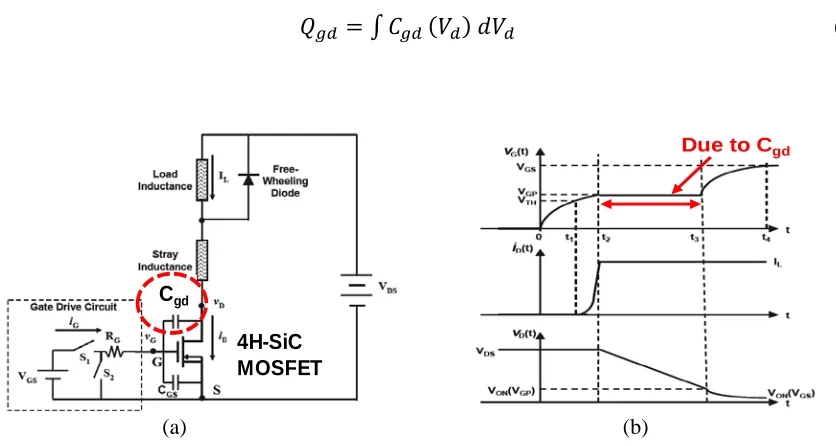
2. Switching Characteristics
It is known that reverse transfer capacitance (Cgd) and gate-to-drain charge (Qgd), resulting
from the gate-to-drain overlap above the JFET region, are the dominant components limiting the
switching capability [7][8]. Figure 1.2(a) shows a clamped inductive load switching circuit
configuration using a free-wheeling diode (high side) and 4H-SiC MOSFET (low side) [2]. The
Cgd of the MOSFET is marked in the figure. Turn-on switching waveforms for gate voltage (Vg),
drain current (Id), and drain voltage (Vd) of the switching circuit are shown in Figure 1.2(b). When
the gate voltage becomes bigger than threshold voltage (Vth), the drain current begins increasing.
When the current reaches to load current, it remains constant and the drain voltage decreases
toward ~0 V. Meanwhile, the gate plateau voltage is observed due to the Cgd charging as marked
in Figure 1.2(b), and the dominant switching energy loss occurs during the plateau. This plateau
time, thus, is directly related to the Cgd values. The Qgd can be obtained from the Cgd as below [2];
𝑄𝑄𝑔𝑔𝑔𝑔 = ∫ 𝐶𝐶𝑔𝑔𝑔𝑔(𝑉𝑉𝑔𝑔) 𝑑𝑑𝑉𝑉𝑔𝑔 (1.3)
(a) (b)
Figure 1.2. (a) Clamped inductive load switching circuit configuration with a free-wheeling diode (high side) and 4H-SiC MOSFET (low side), (b) Turn-on switching waveforms for gate voltage (Vg), drain
current (Id), and drain voltage (Vd) of the switching circuit [2]. 4H-SiC
MOSFET Cgd
4 Here, Vd is the drain voltage. Therefore, in order to reduce the energy loss in high frequency
applications, the MOSFET’s Cgd and Qgd must be minimized because the switching energy loss
mainly originates from their charging (turn-on plateau) and discharging (turn-off plateau) during
each switching cycle [7]. High Frequency Figures-of-Merit (HF-FOMs), defined as [Ron×Cgd] and
[Ron×Qgd], are common high frequency performance indicators [2]. It is important to achieve low
values for the HF-FOMs.
In addition, a gate driver design without false trigger can be achieved with smaller Cgd and
devices with larger FOM [Ciss/Cgd] ratio are desirable to prevent shoot-through current during high
frequency operation [2].
There have been several research reports to reduce the Cgd and Qgd so that the improved
HF-FOMs could be achieved. Cree, Inc. (Wolfspeed) has proposed and demonstrated 4H-SiC
central implant MOSFET (CIMOSFET) structures to improve the Cgd, Qgd, and HF-FOMs in 2015
[9]. This approach requires an additional mask step for p-type ion implantation in the middle of
the JFET region to reduce the gate-to-drain overlap area. Si split-gate and terraced-gate structures
have demonstrated to have the better Cgd, Qgd, and HF-FOMs [7][10][11]. Numerical simulation
studies of a 4H-SiC split-gate MOSFET structure have been presented without any experimental
results in ISPSD 2016 [12].
3. PRESiCE
TMThe Process engineered for manufacturing Silicone Carbide (SiC) electronic-devices
(PRESiCETM) has been set up, established, and successfully qualified at a commercial foundry
company, X-Fab, by running multiple wafer lots on a PowerAmerica project funded by Office of
5 PowerAmerica sponsored the development of PRESiCETM in 2015 for fabricating wide bandgap
power devices such as MOSFETs, JBSFETs, and JBS rectifiers to encourage participation of more
companies in manufacturing devices and to drive the device manufacturing cost down by
increasing the wafer volume at the foundry in the United States.
Figure 1.3(a) shows the fabricated power devices on a 4H-SiC 6-inch wafer using the
PRESiCETM, and the fabricated devices were measured with the semi-automatic Signatone probe
station and Keysight B1505A curve tracer as shown in Figure 1.3(b). Wafer maps and statistical
distributions were created using macro programs out of the measured data from the multiple
(a) (b)
Figure 1.3. (a) Fabricated power devices on a 4H-SiC 6-inch wafer, (b) Semi-automatic Signatone probe station and Keysight B1505A curve tracer.
(a) (b)
Figure 1.4. Wafer map and statistical distribution of the on-resistance of power MOSFETs manufactured using PRESiCETM technology [13].
6 fabricated wafer lots. The NCSU PRESiCETM process has been qualified by comparing those
wafer maps and statistical distributions to each other.
A wafer map of the on-resistance of a typical power MOSFET with the statistical
distribution and a wafer map of the threshold voltage of a typical power MOSFET with the
statistical distribution is shown in Figure 1.4 and Figure 1.5, respectively. The figures demonstrate
that the standard deviations of the device parameters are very small allowing the manufacturing of
power MOSFETs with high yield.
All the designed and optimized 1.2 kV rated 4H-SiC planar gate power MOSFETs for my
entire Ph.D work were fabricated at X-Fab using the qualified PRESiCETM process.
4. Outline of Dissertation
In this dissertation, novel device structure designs, fabrications, and characterizations of
1.2 kV 4H-SiC planar-gate power MOSFETs for the improved HF-FOMs are extensively
discussed. Gate oxide thickness (tOX) of 50 nm and channel length (LCH) of 0.5 µm were fixed for
(a) (b)
Figure 1.5. Wafer map and statistical distribution of the threshold voltage for power MOSFETs manufactured using PRESiCETM technology [13].
7 all the 1.2 kV 4H-SiC Planar-Gate Power MOSFETs throughout this dissertation. The dissertation
consists of total 6 chapters.
Chapter 1 provides the research background and motivation with regard to the 1.2 kV
4H-SiC planar-gate MOSFETs with the improved HF-FOMs.
Chapter 2 presents the optimization of JFET region parameters for the 1.2 kV 4H-SiC linear
cell planar-gate MOSFET to achieve the reduced Cgd, Qgd, and HF-FOMs. The MOSFETs with
various designs in the JFET region were fabricated on 6-inch wafers. Investigations on
on-resistance, Cgd, Qgd, and leakage currents in the forward blocking mode conclude that the optimized
JFET region allows improved HF-FOMs.
Chapter 3 discusses the 1.2 kV-rated 4H-SiC linear cell Split Gate MOSFET
(SG-MOSFET) structure. It has been demonstrated to have superior HF-FOMs with experimental
validation for the first time. Excellent electrical characteristics (specific on-resistance, threshold
voltage, breakdown voltage, Cgd, and Qgd) were measured from devices fabricated on a 6-inch SiC
wafer. Compared to the conventional MOSFET, the SG-MOSFET has 2.4× smaller HF-FOM
[Ron×Qgd] due to the reduced Qgd.
Chapter 4 describes a novel 1.2 kV-rated 4H-SiC linear cell Buffered-Gate MOSFET
(BG-MOSFET) structure. The structure has been intensively studied and experimentally demonstrated
to have superior HF-FOMs for the first time. From the measured data on devices fabricated in a
6-inch foundry, the BG-MOSFET is demonstrated to have 4.0× and 2.6× smaller HF-FOM [Ron×Qgd],
and 3.6× and 2.1× smaller HF-FOM [Ron×Cgd], when compared to the conventional MOSFET and
SG-MOSFET, respectively.
Chapter 5 presents detailed comparisons of the electrical characteristics for the 1.2 kV rated
8 cell topologies fabricated using the same design rules and process flow in a 6-inch foundry for the
first time. TCAD numerical simulations have been conducted to analyze the structures. It has been
observed that the square and hexagonal cell topologies with the same structural dimensions show
similar electrical performance. When compared with the standard linear cell topology: (a) the
hexagonal cell topology has 1.15× better on-resistance and 1.12× worse HF-FOM [Ron×Qgd]; (b)
the octagonal cell topology has 1.5× worse on-resistance and 1.4× better HF-FOM [Ron×Qgd]; (c)
the Split-Gate octagonal cell topology has 1.5× worse on-resistance and 2.3× better HF-FOM
[Ron×Qgd]. In addition, the octagonal cell topologies have a much superior [Ciss/Cgd] FOM to
prevent shoot-through during high frequency switching.
9 REFERENCES
[1] B. J. Baliga, Gallium Nitride and Silicon Carbide Power Devices. Hackensack, NJ, USA:
World Scientific, 2017, ch. 11, pp. 287-340.
[2] B. J. Baliga, Fundamentals of Power Semiconductor Devices 2nd ED. Gewerbestrasse 11,
6330 Cham, Switzerland: Springer, 2019, ch. 6, pp. 283-440.
[3] J. W. Palmour, L. Cheng, V. Pala, E. V. Brunt, D. J. Lichtenwalner, G.-Y. Wang, J.
Richmond, M. O′Loughlin, S. Ryu, S. T. Allen, A. A. Burk, and C. Scozzie, “Silicon Carbide
Power MOSFETs: Breakthrough Performance from 900 V up to 15 kV,” in Proc. 26th Int.
Symp. Power Semiconductor Devices ICs, Jun. 2014, pp. 79-82, doi: 10.1109/ISPSD.2014.6855980.
[4] W. Sung, K. Han, and B. J. Baliga, “Optimization of the JFET region of 1.2kV SiC
MOSFETs for improved high frequency figure of merit (HF-FOM),” in Proc. 5th Workshop on Wide Bandgap Power Devices and Applications (WiPDA), Oct 2017, pp. 238-241, doi:
10.1109/WiPDA.2017.8170553.
[5] http://www.cree.com/Power/Products/MOSFETs.
[6]
http://www.infineon.com/cms/en/product/power/igbt/igbt-discrete/discrete-igbt-with-anti-
parallel-diode/600v-and-1200v-highspeed-3/channel.html?channel=db3a304339536e1401396775983a4bff.
[7] T. Sakai and N. Murakami, “A New VDMOSFET Structure with Reduced Reverse Transfer
Capacitance,” IEEE Trans. Electron Devices, vol. 36, no. 7, pp. 1381-1386, Jul. 1989, doi: 10.1109/16.30945.
[8] J. Wei, M. Zhang, H. Jiang, C.-H. Cheng, and K. J. Chen, “Low ON-Resistance SiC
10 IEEE Electron Device Letters, vol. 37, no. 11, pp. 1572-1577, Nov. 2016, doi:
10.1109/APEC.2010.5433441.
[9] Q. C. J. Zhang, G. Wang, H. Doan, S.-H. Ryu, B. Hull, J. Young, S. Allen, and J. Palmour,
“Latest Results on 1200V 4H-SiC CIMOSFETs with Rsp,on of 3.9mΩ∙cm2 at 150°C,” in
Proc. 27th Int. Symp. Power Semiconductor Devices ICs, May 2015, pp. 89-92, doi: 10.1109/ISPSD.2015.7123396.
[10] Y. Shimada, K. Kato, S. Ikeda, and H. Yoshida, “Low Input Capacitance and Low Loss
VD-MOSFET Rectifier Element,” IEEE Trans. Electron Devices, vol. 29, no. 8, pp. 1332-1334, Aug. 1982, doi: 10.1109/T-ED.1982.20877.
[11] D. Ueda, H. Takagi, and G. Kano, “A New Vertical Double Diffused MOSFET-The
Self-Aligned Terraced-Gate MOSFET,” IEEE Trans. Electron Devices, vol. ED-31, no. 4, pp. 416, Apr. 1984, doi: 10.1109/T-ED.1984.21543.
[12] H. Jiang, J. Wei, X. Dai, M. Ke, C. Zheng, and I. Deviny, “Silicon Carbide Split-Gate
MOSFET with Merged Schottky Barrier Diode and Reduced Switching Loss,” in Proc. 28th
Int. Symp. Power Semiconductor Devices ICs, Jun. 2016, pp. 59-62, doi: 10.1109/ISPSD.2016.7520777.
[13] B. J. Baliga, W. Sung, K. Han, J. Harmon, A. Tucker, and S. Syed, “PRESiCETM: Process
11
CHAPTER 2.
Optimization of 1.2 kV 4H-SiC
Linear Cell Planar-Gate MOSFETs
1. Background & Motivation
1.1. Major Issues of 4H-SiC MOSFETs
Due to the superior material properties, low on-resistance, and fast switching speed with
unipolar current conduction, 4H-SiC MOSFETs have been spotlighted and commercialized
[1][2][3]. Although the 4H-SiC MOSFETs have shown tremendous progresses in the electrical
performances in the past decade, there are still two major performance limiting factors that should
be carefully considered for the structure optimization study [1][2].
High gate oxide electric field is the first performance limiting factor in the 4H-SiC
MOSFETs. Figure 2.1 shows the half-cell cross-sectional view of the 4H-SiC planar-gate power
MOSFETs [2]. During the forward blocking mode, the highest electric field is observed at the
corner of the P+ shielding region in the 4H-SiC and at the center of the gate oxide (“A” in Figure
2.1). SiO2 has been used for the gate oxide in the 4H-SiC MOSFETs because it can be formed
easily with a thermal oxidation process, similar to Si [1][2][4]. Relative dielectric constant for the
SiO2 is 3.9, while that for the 4H-SiC is 9.7 [1]. From the Gauss’s law, the relationship of the
electric field between the SiO2 and 4H-SiC can be found as below;
𝜀𝜀
𝑙𝑙𝑚𝑚∙ 𝜖𝜖𝑙𝑙𝑚𝑚 =𝜀𝜀
4𝐻𝐻−𝑆𝑆𝑆𝑆𝑆𝑆 ∙ 𝜖𝜖4𝐻𝐻−𝑆𝑆𝑆𝑆𝑆𝑆 (2.1)12 These equations indicate that the electric field of the SiO2 becomes 2.5 times bigger than that of
the 4H-SiC at the interface. Although the critical electric field for the SiO2 is about 10 MV/cm, it
is important to keep the electric field less than 4 MV/cm because of reliability issues [4]. Therefore,
the gate oxide electric field should be dealt with carefully when the MOSFET structure is designed.
The second major issue in the 4H-SiC MOSFET is the poor channel mobility. The high
interface trap density, Dit is observed at the interface between the 4H-SiC and thermally grown
gate oxide (“B” in Figure 2.1) due to the C-atom dangling bonds [4]. In recent years, significant
advances have been made with regards to the gate oxide process on the 4H-SiC. Most notably,
high temperature post oxidation annealing process (POA) using nitric oxide (NO) or nitrogen
dioxide (NO2) helps to reduce the Dit, which improves the channel mobility. The nitrided oxide
technique, therefore, has been used for the gate oxidation process by most SiC MOSFET
developers [5]. Nevertheless, the improved channel mobility is much smaller than the bulk
mobility. In addition, there is a trade-off between the channel mobility and threshold voltage [6].
Therefore, it is still the major performance limiting factor in the 4H-SiC MOSFETs.
Figure 2.1. Half-cell cross-sectional view of the 4H-SiC MOSFET structure [2].
13 1.2. Inversion vs. Accumulation Channels
Due to the wide energy bandgap property of 4H-SiC, two different channel modes can be
designed: inversion mode channel (Inv) and accumulation mode channel (Acc) designs. Detailed
information on the design of the channels to achieve a reasonable threshold voltage and field effect
mobility will be discussed in the following sections. The Inv-channel MOSFET (InvFET) and
Acc-channel MOSFET (AccFET) cross-sectional views are shown in Figure 2.2(a) and (b), respectively
[1][2]. For the Acc-channel, constant n-type doping near the top surface needs to be designed to
assure accumulation mode operation. The n-type Acc-channel is completely depleted by the
built-in potential of the junction with the P+ shieldbuilt-ing region underneath the n-type channel (Figure
2.2(b)), creating a potential barrier for electrons at zero gate bias in the blocking mode [1][2][7].
Current transport in the channel occurs with positive gate bias induced accumulation layers to
create an enhancement mode device.
Field effect channel mobilities of 4H-SiC AccFETs and InvFETs at high temperatures are
shown in Figure 2.3(a) [6]. The channel mobilities were measured from lateral MOSFET structures
at high temperatures up to 200°C. It indicates that the channel mobility for the Acc-channel
structures is over 20 cm2/Vs at room temperature, which is about 2 times higher than that of the
(a) (b)
14 Inv-channel structures. In addition, both Acc- and Inv-channel mobilities increase as temperature
rises as shown in Figure 2.3(a). The increase in absolute value of the channel mobility is about the
same for both structures. The higher channel mobility for the AccFETs improves the channel
resistance, leading to the reduced total specific on-resistance when compared to the InvFETs [6].
It should be noted that there is a trade-off between the channel mobility and threshold
voltage. A clear correlation between the channel mobility and threshold voltage has been found
for both AccFETs and InvFETs as shown in Figure 2.3(b) [6]. This result indicates that the
AccFETs can have larger channel mobility at an acceptable threshold voltage with the carefully
designed channel structure.
Figure 2.4 shows the electrostatic potential simulation results near the gate oxide interface
along with X dimension for (a) Acc and (b) Inv MOSFETs with the channel length of 0.3 µm at
Vd=1200 V and Vg=0 V. The channel barriers are shown in the figure. The results indicate that
Acc-channel MOSFETs have smaller channel barriers than Inv-channel devices, resulting in
inevitable larger leakage current inherently [1]. Although the AccFETs have a little bit higher
leakage current than InvFETs due to the smaller channel barrier, that is still well below the standard
(a) (b)
Figure 2.3. (a) Field effect channel mobilities of SiC AccFETs and InvFETs at high temperatures, (b) Trade-off between channel mobility and threshold voltages [6].
0 5 10 15 20 25
25 50 75 100 125 150 175 200
Cha
nne
l m
obi
lit
y (
cm
2/V
s)
15 industry leakage current of 100 µA. These behaviors will be discussed in detail with experimental
results in the next chapter.
2. Structure Optimization
Asmita Saha and James A. Cooper have published a research paper regarding the 1
kV-rated 4H-SiC power MOSFET structure optimization in 2007 as shown in Figure 2.5 [8]. The study
(a) (b)
Figure 2.4. Electrostatic potential simulation results along with X dimension for (a) Acc and (b) Inv MOSFETs with the channel length of 0.3µm at Vd=1200V and Vg=0V. The channel barriers are shown in
the figure.
2.1 V
N+ source P-base
1.2 V
N+ source N-base
(a) (b)
16 mainly focused on reducing the on-resistance (Ron) with optimization of the JFET region, current
spreading layer (CSL), and source contact area using a figure-of-merit, defined as [BV2/R on,sp],
where Ron,sp is Ron multiplied by a device active area. However, other important electrical
characteristics such as capacitance and gate charge are not discussed in the paper. For the improved
high speed and high frequency capability in the SiC MOSFETs, it is necessary to reduce the reverse
transfer capacitance (Cgd) and gate-to-drain charge (Qgd) as well as the Ron by conducting the
structural optimization as mentioned in the previous chapter.
2.1. JFET Region Optimization
In this chapter, the optimization of the JFET region for the conventional planar MOSFET
will be mainly focused with emphasis on HF-FOMs, [Ron×Cgd] and [Ron×Qgd], because the JFET
region optimization has a direct impact on Cgd and Qgd as well as Ron as shown in (2.3), (2.4), and
(2.5) below [1][2];
,
, OX S M gd JFET Cell
OX S M
C C
C W Z
C C
= ⋅ ⋅ +
(2.3)
( )
gd gd d d
Q
=
∫
C
V
dV
(2.4). .
2 where,
JFET S bi
JFET dep
JFET dep JFET
V
R W
W W qN
ρ ε
∝ =
− (2.5)
where WJFET is the JFET width (shown in Figure 2.6), ZCell is the unit cell length orthorgonal to
the cross section. COX and CS,M are the gate oxide capacitance and semiconductor capacitance,
17 εS is the SiC dielectric constant, Vbi is the built-in potential, and NJFET is the JFET region doping
concentration. As shown in (2.3) and (2.4), the Cgd is proportional to the WJFET and the Qgd is
directly related to the WJFET because the Qgd is obtained by the integral of the Cgd with respect to
Vd (Drain voltage). Therefore, the reduced Cgd and Qgd can be achieved with the narrower JFET
width. In addtion to the Cgd and Qgd, the narrow WJFET helps to reduce the gate oxide electric field
by a screening effect of the P+ shielding region [1].
However, the narrow WJFET increases the Ron. The Ron consists of source and drain contact
resistance (RC), N+ source resistance (RS), channel resistance (RCH), JFET resistance (RJFET), drift
resistance (RDR), and substrate resistance (RSUB) as shown in Figure 2.6 [2]. The RJFET is inversely
proportional to the WJFET (2.5), so the narrow WJFET has bad effect on the electron flow in the JFET
region, which causes the increase of the Ron. By increasing the doping concentration in the JFET
region (NJFET), the Ron can be maintained low at the narrower JFET width due to the reduced ρJFET
and Wdep as shown in (2.5).
Therefore, the JFET optimization should be carried out in accordance with the balance
between the JFET width and JFET doping concentration to achieve the optimized Cgd, Qgd, gate
oxide electric field less than 4 MV/cm, and Ron.
Figure 2.6. Unit cell cross sectional view of the 4H-SiC MOSFET [4] with series resistance components and reverse transfer capacitance (Cgd).
Cgd
WJFET
Wdep.
18 2.2. Analysis with Analytical Models
In this section, the Ron,sp of the conventional linear cell SiC MOSFET structures with
various WJFET is analyzed using the analytical models which are available in [1][2]. Among the
numerous series resistance components mentioned earlier, the only Rch,sp, Rdrift,sp, and RJFET,sp will
be considered because they are the major contribution sources to the Ron [9].
Figure 2.7 shows the cross-sectional view of the 1.2 kV-rated 4H-SiC conventional Acc-
or Inv-channel MOSFETs with pertinent structural information. The P+ contact is in the orthogonal
direction to the cross-section to reduce the cell pitch (WCell). For the analytical calculations, the
channel mobility (µch,FE) of 21 cm2/V⋅s for the Acc-channel or 13 cm2/V⋅s for the Inv-channel
structure measured at room temperature is used as discussed in the previous section (Figure 2.3(a)).
The analytical models for the Rch,sp, Rdrift,sp, and RJFET,sp are as below [1][2];
2 ,
,
[ cm ]
( )
CH Halfcell ch sp
CH FE OX g th
L W
R
C V V
µ
⋅
= Ω ⋅
− (2.6)
Figure 2.7. Cross sectional view of the 1.2 kV-rated 4H-SiC MOSFET with detailed structural parameter information.
Gate
N- Drift :
Doping = 8 x 1015cm-3
Thickness = 10 µm
P+ Shielding N+ source N+ sub Drain Gate Source JFET Base WJFET LCH LN+ WCell WC Structural Parameters CH.
type Accumulation or Inversion WC
[µm] 0.5
LN+
[µm] 1.6 LCH
[µm] 0.5
JFET doping
[cm-3] 8x10 15 3x1016 tOX
19 2
, .
.
ln Halfcell ( ( ) ) [ cm ]
drift sp Drift Halfcell Drift Halfcell JFET dep JFET dep
W
R W t W W W
W W
ρ ρ
= ⋅ ⋅ + − − − Ω⋅
−
(2.7)
2 ,
.
[ cm ]
JFET P Cell JFET sp JFET dep t W R W W ρ ⋅ +⋅ = Ω⋅ − (2.8)
where COX is the oxide capacitance, Vg is the applied gate voltage, Vth is the threshold voltage,
ρJFET is the resistivity of the JFET region, tp+ is the junction depth of the P+ shielding region, Wdep.
is the depletion width in the JFET region, ρDrift is the resistivity of the drift region, and t is the drift
region thickness.
The analytically calculated Ron,sp with Rch,sp, Rdrift,sp, and RJFET,sp for the conventional
Acc-channel MOSFETs having the various WJFET is plotted in Figure 2.8. The analytical calculations
for the structures without (NJFET = 8×1015 cm-3) and with the enhanced JFET doping concentration
(NJFET = 3×1016 cm-3) are shown in Figure 2.8(a) and (b), respectively. As expected, the Ron,sp is
increased when the WJFET is reduced because the RJFET,sp and Rdrift,sp are increased. The increase of
(a) (b)
Figure 2.8. Analytically calculated Ron,sp with Rch,sp, Rdrift,sp, and RJFET,sp for the conventional MOSFETs having
various WJFET and NJFET of (a) 8×1015 cm-3 and (b) 3×1016 cm-3. 0.00
2.00 4.00 6.00 8.00
0.5 1.5 2.5
R on ,s p (m Ohm -c m 2)
Width of JFET region (um)
@NJFET= 8×1015cm-3
RTotal
Rdrift, sp
Rch, sp
RJFET, sp 0.00
2.00 4.00 6.00 8.00
0.5 1.5 2.5
R on ,s p (m Ohm -c m 2 )
Width of JFET region (um)
@NJFET= 3×1016cm-3
RTotal
Rdrift, sp
Rch, sp
20 the Rdrift,sp with the narrower WJFET is resulted from current spreading for the current conduction
below the P+ shielding region [1][2]. The increased RJFET,sp and Rdrift,sp with narrower WJFET can
be mitigated by the enhanced JFET doping of 3×1016 cm-3 as shown in Figure 2.8(b). Thereby, the
total Ron,sp for the MOSFETs with narrow WJFET can be kept low.
The measured µCH,FE from the lateral Acc and Inv mode MOSFET structures with LCH of
200 µm [6] is compared with the analytically calculated drift region mobility (µDrift) up to 150°C
in Figure 2.9 [9]. The µDrift was calculated using [4];
2.7 2
Drift 17 0.6
Drift
1020
= [cm /V s]
1 ( / 1.8 10 ) 300 T N
µ ⋅ − ⋅
+ × (2.9)
where NDrift is the drift region doping concentration and T is the junction temperature. The µDrift
decreases rapidly, while the measured µCH,FE for both of the Acc and Inv structures increases, with
increasing temperature as shown in Figure 2.9.
Figure 2.9. Measured channel mobilities (µCH,FE) for Acc and Inv MOSFETs and analytically calculated
drift region mobilities (µDrift) at high temperatures [9].
0 150 300 450 600 750 900 0 5 10 15 20 25 30
0 25 50 75 100 125 150 175
µ
Dr ift(cm
2/V
-s)
µ
CH ,FE(cm
2/V
-s)
Temperature (
°
C)
21 Figure 2.10 compares the calculated Rch, RJFET, and Rdrift resistances for Inv and Acc
MOSFETs with various WJFET and enhanced NJFET (3×1016 cm-3) at (a) 25°C and (b) 150°C [9].
The RJFET and Rdrift increase with temperatures due to a reduction in bulk mobility, while the Rch
decreases due to an increase in channel mobility (Figure 2.9). Consequently, the contribution of
RJFET and Rdrift to Ron becomes larger from 25°C to 150°C for both of the Acc and Inv MOSFETs
as shown in Figure 2.10(a) and (b), leading to an increase of Ron at 150°C.
Analytically calculated increase in the ratio [Ron(150°C)/Ron(25°C)] for Acc and Inv
MOSFETs with various JFET widths is shown in Figure 2.11 [9]. The ratio becomes greater with
narrower JFET width for both of the MOSFETs because of the bigger RJFET and Rdrift portions as
shown in Figure 2.11. In addition, the increase in the ratio is smaller in the Inv structures than in
the Acc structures overall due to more balanced Rjfet, Rdrift, and Rch with increasing temperature.
These analytical calculations will be compared with the actual experimental data in the following
section.
(a) (b)
Figure 2.10. Comparison of Rch, Rjfet, and Rdrift components using analytical models for Acc and Inv
MOSFETs with various JFET widths at (a) 25°C and (b) 150°C. The contribution of Rjfet and Rdrift to Ron
becomes larger than Rch at narrower JFET width. The impact is greater in the Acc structures [9].
0% 20% 40% 60% 80% 100% 0. 5 0. 8 1. 1 1. 4 1. 7 2. 0
W
JFET(
µ
m)
Acc.
0. 5 0. 8 1. 1 1. 4 1. 7 2. 0W
JFET(
µ
m)
Inv.
0% 20% 40% 60% 80% 100% 0. 5 0. 8 1. 1 1. 4 1. 7 2. 0W
JFET(
µ
m)
Acc.
0. 5 0. 8 1. 1 1. 4 1. 7 2. 0W
JFET(
µ
m)
Inv.
22 2.3. TCAD Numerical Simulations
TCAD numerical simulations were performed for the 1.2 kV-rated SiC conventional planar
power MOSFETs. All the structures have the Acc-channel and same structural parameters except
for the WJFET and NJFET as described in Figure 2.7.
The Breakdown Voltage (BV) simulations were conducted as a function of the NJFET and
WJFET with the oxide field limitation of 4 MV/cm as shown in Figure 2.12(a). The BV of 1700 V
was observed for the devices with the WJFET of 0.6 µm regardless of the NJFET. However, when the
WJFET becomes large, the BV with the higher NJFET gets reduced because of the oxide field
limitation. Therefore, the NJFET less than 4×1016 cm-3 is required to achieve the high enough BV
for the structures with wide WJFET.
The oxide electric field should be carefully examined to determine the WJFET because the
electric field at the gate oxide increases with enhanced JFET doping as already discussed in Figure
2.12(a). The oxide electric field simulations for the structures with the enhanced JFET doping of
3×1016 cm-3 were performed at Vd of 1600 V as shown in Figure 2.12(b). In order to keep the oxide
Figure 2.11. Analytically calculated increase in the ratio [Ron(150oC)/Ron(25oC)] for Acc and Inv MOSFETs
with various JFET widths. The ratio is bigger when the JFET width becomes smaller [9].
1.0 1.2 1.4 1.6 1.8 2.0 2.2
0.5 0.8 1.1 1.4 1.7 2.0
Rat
io
[R
on
(150)
/R
on
(2
5)]

![Figure 2.20. Typical output characteristics for Acc MOSFET_J_0.7 and MOSFET_1.1 measured at Vg from 0 to 25 V with 5 V steps at room temperature [10]](https://thumb-us.123doks.com/thumbv2/123dok_us/1330003.1165952/51.612.123.487.372.660/figure-typical-output-characteristics-mosfet-mosfet-measured-temperature.webp)


![Figure 2.27. Comparison of blocking capability. MOSFETs with narrower JFET widths (MOSFET_J_0.7) show lower leakage currents [10]](https://thumb-us.123doks.com/thumbv2/123dok_us/1330003.1165952/56.612.127.486.454.679/figure-comparison-blocking-capability-mosfets-narrower-mosfet-currents.webp)
![Figure 2.29. Normalized Ron from measured output characteristics of the fabricated Acc and Inv-channel SiC MOSFETs with different JFET widths (0.7, 1.1, 1.5 µm) [9]](https://thumb-us.123doks.com/thumbv2/123dok_us/1330003.1165952/57.612.126.488.463.679/figure-normalized-measured-characteristics-fabricated-channel-mosfets-different.webp)