A Comparative Analysis of Delay Based PUF
Implementations on FPGA
Sergey Morozov, Abhranil Maiti, Patrick Schaumont, Virginia Polytechnic Institute and State University
{morozovs, abhranil, schaum}@vt.edu
Abstract. Physical Unclonable Functions promise cheap, efficient, and secure identification and authentication of devices. In FPGA devices, PUFs may be instantiated directly from FPGA fabric components in order to exploit the propagation delay differences of signals caused by manufacturing process variations. Multiple delay based PUF architectures have been proposed. However, we have observed inconsistent results among them. Ring Oscillator PUF works fine, while other delay based PUFs show a significantly lower quality. Rather than proposing complex system level solutions, we focus on the fundamental building blocks of the PUF. In our effort to compare the various delay based PUF architectures, we have closely examined how each architecture maps into the FPGA fabric. Our conclusions are that arbiter and butterfly PUF architectures are ill suited for FPGAs, because delay skew due to routing asymmetry is over 10 times higher than the random variation due to manufacturing process. On the other hand, ring oscillator PUF does not suffer from the same limitations.
Keywords: Physical Unclonable Functions (PUF), process variation, FPGA routing, delay, arbiter, ring oscillator, butterfly.
1 Introduction
A Physical Unclonable Function (PUF) has the unique advantage of generating volatile chip-specific signatures at runtime. It not only excludes the need of an expensive non-volatile memory for key storage, but also offers robust security shield against attacks. It is emerging as a promising solution to issues like intellectual property (IP) protection, device authentication, and user data privacy. The IP protection issue on FPGA platform is specially a critical one due to the reconfigurable nature of the FPGA devices. A PUF can potentially resolve this issue by creating device-specific IPs using device-specific signature. Similarly, other security related issues can be addressed using a PUF.
present the critical factors that need to be considered by the designer while implementing a delay-based PUF on FPGA.
The majority of the PUF designs is based on delay variation of logic and interconnect. We analyze three delay based architectures, namely, Arbiter PUF, Ring Oscillator PUF and Butterfly PUF. The fundamental principle followed in a delay-based PUF is to compare a pair of structurally identical/symmetric circuit elements (composed of logic and interconnect), and measure any delay mismatch that is introduced by the manufacturing process variation, and not by the design. This essentially requires identical/symmetrical implementation for the two compared circuit elements in consideration. This can be best achieved by VLSI level placement and routing techniques. However, VLSI level circuit manipulation techniques cannot be used because implementation of circuits on FPGA is a post fabrication process. Moreover, the lack of information regarding the underlying VLSI layout of the reconfigurable fabric limits the design space to FPGA components such as lookup tables and storage. At this level, achieving symmetry in circuit elements is not only difficult, but also requires many assumptions about the FPGA structure. Additionally, the limitations of standard FPGA design tools to control low-level placement and routing make a PUF design somewhat complex in nature.
We will show that Arbiter PUF and Butterfly PUF largely suffer from the above limitations, and an effective implementation of these two PUFs is difficult on FPGA. The delay skew, inherently present between a pair of circuit elements that are required to be symmetric in these PUFs, is an order of magnitude higher than the delay variation due to random process variation. On the other hand, the architecture of a ring oscillator based PUF is independent of these limitations, and thus allows for an easy implementation on FPGA. Our main contribution in this paper is to present a detailed comparative analysis of the implementation complexities of these three PUFs on a 90nm commodity FPGA platform.
The rest of the paper is organized as follows. Section 2 briefly discusses the basic definition of a PUF and various PUF techniques. It also includes a delay model of the PUF interconnects, and a structural comparison of the three PUFs. Section 3 describes some necessary architectural information of a Xilinx Spartan 3E FPGA which we used as the reference platform. In section 4, we present our detailed analysis of the PUF implementation complexities. Finally, in section 5 we conclude the paper.
2 Background
2.1 CMOS PUFs
Extraction and characterization of the static process variation out of a CMOS device is the underlying principle of an on-chip PUF circuit. On-chip PUF techniques either exploit components such as SRAM cells [1, 2], FPGA configuration memory [3] or add a specialized circuit to extract the process variation imprint. In analyzing the design complexity, we will consider only the last type. This category of PUF is mainly based on the delay variation of logics and interconnects, and we focus on three existing techniques of this category – arbiter PUF (APUF), ring oscillator PUF (ROPUF) and Butterfly PUF (BPUF).
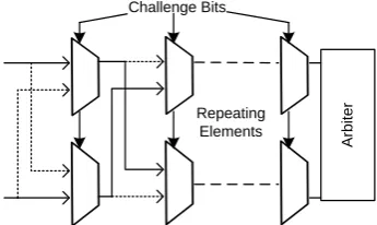
Arbiter PUF – An APUF, proposed by Lim et.al [4], is composed of two identically configured delay paths that are stimulated by an activating signal. The difference in the propagation delay of the signal in the two delay paths is measured by an edge triggered flip-flop known as the arbiter. The delay difference is a function of the manufacturing process variation present in the delay paths. Several PUF response bits can be generated by configuring the delay paths in multiple ways using the challenge inputs. An APUF scheme is shown in Figure 1.
Fig. 1. An arbiter PUF scheme with several switches and an arbiter.
Ring Oscillator PUF – In an ROPUF [5], variations in frequencies of several identically laid out ring oscillators are exploited to build the PUF. The RO frequencies are captured in a counter, and are subsequently transformed into binary outputs by a simple comparison method.
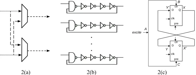
Butterfly PUF – The Butterfly PUF, proposed by Kumar et.al [6], is a technique that aims to emulate the behavior of an SRAM PUF [1]. However, the functionality of this PUF is based on the delay variations of interconnects unlike the SRAM PUF where the variation in threshold voltage of transistors is the key factor. A BPUF cell employs two cross-coupled latches, and exploits the random assignment of a stable state from an unstable state that is forcefully imposed by holding one latch in preset while the other in clear mode by an excite signal (Figure 3(c)). The final state is determined by the random delay mismatch in the pair of feedback paths and the excite signal paths due to process variation.
A
rb
it
e
r
Challenge Bits
2.2 Delay Model in Delay Based PUFs
The main idea of this work is to analyze the implementation complexities of the three delay-based PUF architectures, namely, APUF, ROPUF and BPUF. In order to do that, we first introduce a delay model for the PUF interconnect. We define the delay d
of a net in Equation 1, where dS is the static delay as determined by the static timing
analysis tools, and dR is the random delay component due to process variation.
d = dS + dR (1)
In a delay based PUF, let us consider two nets N1 and N2 that need to be compared.
The delay values for the two nets are defined as follows.
d (N1)= dS1 + dR1
d (N2) = dS2 + dR2
(2) (3) If the two nets have identical layout, then we can assume dS1 = dS2. As a result, the
delay skew Δd between N1 and N2 can be expressed as follows.
Δd = d1 – d2 = dR1 – dR2 = ΔdR (4)
This is the ideal case for a delay based PUF where the delay skew is purely a function of the random delay component. The output of the PUF, in this case, will be dependent entirely on the delay difference due to process variation. However, if N1
and N2 are not identically laid out, it is more likely that we have dS1 ≠ dS2. As a result,
delay skew becomes:
Δd = dS1 – dS2 + dR1 – dR2 = ΔdS + ΔdR (5)
In such case, the output of a given PUF structure will be at least partially dependent on ΔdS, causing the output to be biased. Further, if ΔdS > ΔdR, the effect of random
variation becomes insignificant, and the output of the PUF structure becomes static regardless of dR.
For an efficient PUF implementation, the designer should achieve a routing such that ΔdS→ 0. In an ASIC environment, this is easier to implement using VLSI layout.
However, in an FPGA, static timing values provided by the timing analysis tools are the only available delay estimates that a designer can access. We will show that using existing FPGA routing resources, it is very difficult to achieve the condition such that
ΔdS→ 0. As a result, those PUF techniques that strictly depend on this condition are
2.3 Structural Comparison among APUF, ROPUF and BPUF
A delay-based PUF circuit involves extraction and comparison of the random delay,
dR. The effectiveness of the PUF depends on how much symmetry we can achieve
between a particular pair of elements in order to minimize the effect of ΔdS in
Equation 5. This symmetry requirement is different in nature from one PUF technique to another, and determines the implementation complexity of a PUF on FPGA. Independent of the implementation platform, we first analyze the elementary building blocks of the three PUFs to present the inherent symmetry requirement that eventually leads to the implementation complexity.
In Figure 2(a), the switch which is the main building block of the APUF, is shown. The pairs of nets connected to the multiplexers (pairs shown with different patterns) need to be symmetric in order to minimize ΔdS. In Figure 2(b), multiple instances of a
ring oscillator loop are shown. It can be noticed that there is no symmetric pair of components involved in an individual RO loop. In this case, the value of ΔdS between
a pair of RO loops needs to be minimized. As a result, each of these RO loops needs to be identical. In figure 2(c), a BPUF cell is presented. For a functional BPUF, the pair of nets AB/AC as well as XY/X’Y’ need to be symmetric along with the latches.
. . .
2(a) 2(b) 2(c)
Fig. 2. (a). A switch with two multiplexers and delay paths in Arbiter PUF. The symmetric pairs of components are highlighted with matching patterns. (b) Multiple instances of a basic five stage ring oscillator loop for a ROPUF (c) A BPUF cell with two cross coupled latches.
Table 1 shows a brief summary of the routing requirements of the three PUFs. This shows that careful routing is required for APUF and BPUF while creating their respective building blocks. On the other hand, an oscillator loop for an ROPUF does not require any such design constraint. Instead, it requires identical instantiations of RO loops. In section 4, we will show that this fundamental structural difference causes complexity in PUF implementation on FPGA. The pair of multiplexers in an APUF as well as a pair of latches in a BPUF cell needs to be identical, too. However, this is not difficult to achieve. Hence, we focus on the interconnect issue.
Table 1. Summary of comparison among APUF, ROPUF and BPUF.
APUF ROPUF BPUF
A
B
C Y’
X’ Y
X
clk
clk clr
clr D
D Q
Q pre
Requires symmetric routing in a building
block.
Does not require symmetric
routing in a building block. Requires symmetric routing in a building block. Identical instantiation of
building blocks may not be necessary.
Building blocks require identical instantiation.
Identical instantiation of building blocks may not be
necessary.
3 FPGA Architecture and Resources
Before we can explain how the previously described PUF architectures map into an FPGA, we must closely examine the resources available in an FPGA device. We describe the architecture of a Xilinx Spartan3E FPGA device that we used as a platform in our experiments.
Like many commercial FPGA devices, the Spartan 3E FPGAs follow island-style architecture. In this architecture, the primary FPGA resources can be separated into two categories: logic blocks (referred to as Configurable Logic Blocks, CLBs) and routing resources (interconnect). Each CLB is surrounded by and interfaced with a "sea" of interconnect, hence the name. The CLB itself is composed of sub-blocks of logic elements, called slices in Xilinx architectures. Each slice is composed of a lookup table, configurable flip-flops and other logic, and connects to the CLB through ports. We will not focus on the internal structure of the logic elements further, because it is the routing resources that prove to be more important to the construction of PUFs. An important observation is that different resources are often not accessible through the same port of a slice, so routing is specific to the CLB, slice, and port simultaneously.
Any given route in an FPGA is composed of multiple segments, called arcs. For example, there are over 100 arcs going into and coming out of each CLB. The majority of arcs are unidirectional, meaning they can only propagate a signal one way. Arcs begin and terminate at components referred to as Programmable Interconnection Points (PIPs). Any given PIP has a varied number of arcs terminating at it and a varied number of arcs originating from it. During the FPGA configuration, PIPs are activated in a particular way to create the signal routes out of multiple arcs: a PIP is "turned on" with a certain configuration in order to bridge a terminating arc with one or more originating arc. There can only be one driver signal for any particular arc, though it is possible for one signal to fanout and drive multiple arcs. Each PIP is associated with a CLB, and all the PIPs for a particular CLB combine to form a virtual structure referred to as a switchbox. PIP functionality varies: some bridge signals to and from adjacent CLBs creating inter-CLB route, while others direct the signals through switchbox to other local slices, creating an intra-CLB route.
3.1 Routing Complexity
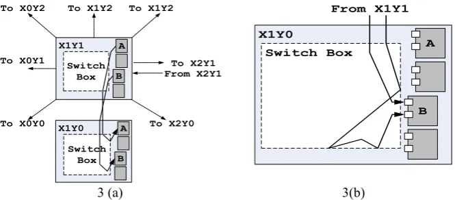
Inter-CLB Routing - At first glance the examination of inter-CLB routing appears promising: there exist direct routes to all adjacent CLBs in most of the FPGA as shown in Figure 3(a). This gives us a large design space for our circuits. It also means that the potential for the required symmetry exists: a signal originating from CLB X1Y1 can be routed to CLB X2Y1, while a signal from CLB X2Y1 can be routed to CLB X1Y1. However further examination of these routes indicate that the PIPs and the arcs employed in implementing these routes are not necessarily symmetric, and can lead to a timing imbalance in the circuits. Moreover, even if the inter-CLB route appears to be symmetric in the FPGA design tool, we can draw no conclusion as to the delay of the route. Even near identical looking routes between slice A and slice B created by the routing software may differ in their estimated delay. Further, not all ports are equal: if a signal must go into a specific port to reach some logic element, the routing for it may differ significantly for other ports of the same slice as in Figure 3(b).
Intra-CLB Routing – Similar observations are found in case of intra-CLB routing as well. All the slices belonging to a particular CLB have identical input and output nets. Connection among these slices can be configured using a specific set of PIPs. However, similar connection between a pair of slices does not necessarily results in same delay. For example, the connection from an output port, say out1, of slice A to an input port, say in1 of slice B may not have the same delay as the delay of the connection from out1 of slice B to in1 of slice A. Yet this type of configuration is often required in a PUF implementation.
X1Y0
Switch Box A
B From X1Y1
3 (a) 3(b)
Fig. 3. (a)Possible inter-CLB routes from a given CLB include all 8 adjacent squares. Routes A to A and B to B may differ in timing. (b) Routing to the ports of the same slice may differ.
4 Analysis of PUF Implementation Complexity
In this section we discuss our experiments, as well as the associated analysis of Arbiter PUF, Butterfly PUF and RO PUF.
X1Y1 A
B Switch
Box
To X0Y0 To X2Y0
To X0Y1
To X0Y2 To X1Y2 To X1Y2
X1Y0
Switch Box
A
B
4.1 Arbiter PUF
The two primary components required for the Arbiter PUF architecture are the switches and the arbiter itself. A useful secondary component is a delay element: trivial logic that inserts additional delay into the paths. By design, the arbiter PUF must route the internal signals through long identical paths in order to extract the manufacturing variation in these paths. This lends the PUF to an inter-CLB design.
We used identical 2-input MUXes in two different slices for the switches. The arbiter was instantiated as a positive clock-edge triggered flipflop in a slice. A look-up table in a slice served as the delay element.
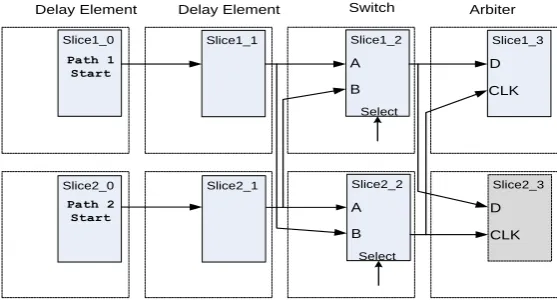
The first mapping scheme that we considered was the Parallel CLB scheme shown in Figure 4. Under this scheme the two paths are located in parallel CLBs, with routes crossing between the two CLBs to create the crossing switch route and one of the arbiter routes. Notice that there are 2 possible locations for the arbiter in this scheme; we considered both. We tested this scheme in four configurations, altering the direction of the path in the chip: East to West, West to East, North to South, and South to North.
Slice1_0
Delay Element Switch
Delay Element Arbiter
Slice1_3
D
CLK
Slice2_3 Slice2_0 Slice2_1
Slice1_1
Select Slice2_2
A
B
Select Slice1_2
A
B
Select
D
CLK
Path 1 Start
Path 2 Start
Fig. 4. Circuit used to analyze the routing properties of APUF paths. The doted white rectangles denote a CLB. The shaded rectangles denote an individual slice. Slice2_3 is an alternative location for the arbiter.
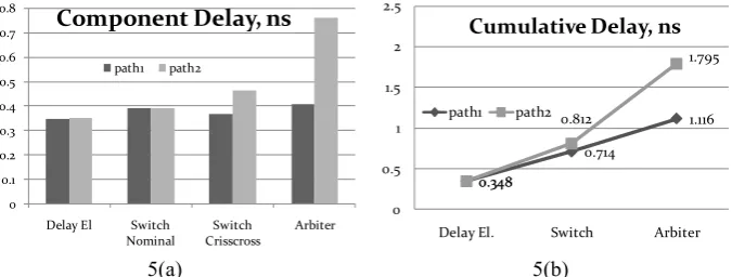
5(a) 5(b)
Fig. 5. (a) Individual delays of each component. (b). Cumulative delay of the path through after each component.
These results indicate that this PUF structure will not function. The 3σ value of delay variation due to process variability in 90 nm technology has been estimated to be approximately 3.5% [7]. On the other hand, we observe that in this case, variation due to routing is much higher than expected variation due to process variability: ΔdS /
ΔdR is 25.6 times. There are two causes of routing variation in this design: the
asymmetric routes for the switch crisscrossing paths and the much more dramatic asymmetric routes to the arbiter. The larger difference in arbiter routes is due to the fact that routing to a CLK input of a flipflop requires sending the signal through multiple additional segments to reach the CLK port, whereas the route to the D input of the flipflop is comparatively simple.
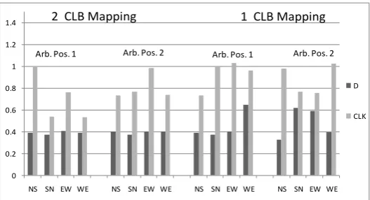
All 4 directions using this mapping produced similar results. While some directions significantly reduced the routing delay, a difference of at least 100 ps remained. We also considered a 2nd mapping architecture where the slices were located in the same CLB, rather than parallel. We hoped that this would reduce the asymmetry in arbiter delay. However, this did not produce a noticeable improvement. Moreover, this mapping introduced a routing imbalance in the delay elements and nominal switch paths. Figure 6 shows the delays we observed for the arbiter component in each direction, depending on the location of the arbiter, and the mapping scheme. Under the best possible conditions of 2 CLB mapping and West to East placement we observe ΔdS / ΔdR to be 11.6 times.
0 0.1 0.2 0.3 0.4 0.5 0.6 0.7 0.8
Delay El Switch Nominal
Switch Crisscross
Arbiter
Component Delay, ns
path1 path2
0.348
0.714
1.116
0.348
0.812
1.795
0 0.5 1 1.5 2 2.5
Delay El. Switch Arbiter Cumulative Delay, ns
Fig. 6. Delay difference in routing to the D input and the CLK input of a slice under various conditions. NS – North to South layout; SN – South to North; EW – East to Wes; WE – West to East.
These results indicate that additional delay due to the complexity of routing a signal to the CLK input of a flipflop cannot be avoided using current routing schemes and architectures. Asymmetry in routing of crisscrossing switch routes is also present, but that delay difference is dwarfed by the arbiter. Additional mapping schemes exist, but any schemes not utilizing parallel CLBs runs a high chance of introducing routing delay in other components. The possibility of trying to balance out the delays of the arbiter paths seems low, since all the elements examined here introduce delays on the order of hundreds of picoseconds themselves. Trying to balance out the delays using these building blocks is unlikely to produce an architecture that allows us to observe the delay variation due to process variability.
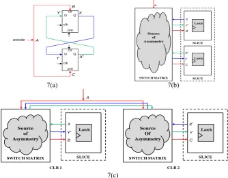
4.2 Butterfly PUF
The effectiveness of the Butterfly PUF is fundamentally based on the symmetry of interconnects between the two latches. In the figure 7(a), the net AB and AC are required to be symmetric for the proposed functionality of the BPUF. Similarly, the pair of nets XY and X’Y’ also needs to be symmetric. While mapping a BPUF cell into FPGA, two latches can be instantiated in the dedicated latch in the slices. It can be safely assumed that two latches at the same position of two different slices are identical since the slices have identical components and ports.
0 0.2 0.4 0.6 0.8 1 1.2 1.4
NS SN EW WE NS SN EW WE NS SN EW WE NS SN EW WE D
CLK
2 CLB Mapping
Arb. Pos. 1
1 CLB Mapping
Arb. Pos. 1
7(a) 7(b)
7(c)
Fig. 7. (a). Circuit structure of BPUF cell. (b) Intra-CLB BPUF mapping (c) Inter-CLB BPUF mapping.
However, the real design challenge comes when a designer has to ensure that the interconnection pairs (XX’/YY’ and AB/AC) are symmetric. Since no layout level information inside the switch box is available, we depend on the static delay values provided by the design tool. Figure 7(b) and figure 7(c) represent how a BPUF cell can be mapped into an FPGA device. Figure 7(b) shows the case when both the latches are implemented inside a single CLB. Another way of implementing would be to place the latches in two different CLBs as shown in figure 7(c).
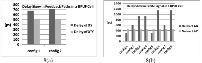
During the automatic routing executed by the design tool, arbitrary PIP connections are assigned leading to different delay values of the nets. A strict timing constraint on the pair of nets to be matched can partially solve this problem. However, based on the availability of the routing resources, this often doesn’t produce the best result. In figure 8, we present a set of data showing the delay skew in the pair of nets AB/AC and XY/X’Y’ (refer to figure 7(a)) as a result of automatic routing with timing constraint for an intra-CLB mapping. For the delay skew in XY/X’Y’ net pair, the minimum value of the ratio ΔdS / ΔdR is estimated to be 17 whereas the same
quantity for the delay skew in AB/AC is 16. Since ΔdS is an order of magnitude
higher than ΔdR, it is obvious that this PUF implementation will produce highly
biased outputs. A B C Y’ X’ Y X clk clk clr clr D D Q Q pre pre excite SLICE SLICE Latch Latch X Y’ B X’ Y C SWITCH MATRIX A Source of Asymmetry SLICE Latch X Y’ B
SWITCH MATRIX SWITCH MATRIX SLICE
Latch X’ Y C A Source of Asymmetry Source Of Asymmetry
8(a) 8(b)
Fig. 8. (a). The delay values of nets XY and X’Y’. Two configurations correspond to two possible placements of the pair of latches inside a CLB. (b) The delay values of nets AB and AC. Eight configurations correspond to four possible placements of the excite signal buffer in a CLB for each of the two possible placements of the latches in the CLB.
Manual routing by manipulating the PIP settings can ensure identical routing configuration. However, it is observed that even in this case, the delay of a pair of interconnects do not match based on the static delay values provided by the design tool. This is the reason why we refer the switch box as the source of asymmetry as shown by the cloud in the figure 7(b) and 7(c).
From figure 7(b) and 7(c), it is evident that both intra-CLB and inter-CLB configuration of a BPUF cell suffers from the asymmetric nature of the FPGA routing resources. Thus, our observations contradict the results presented in [6]. However, we note that our experiments have been done on a Spartan-3E FPGA, and not on a Virtex-5 as used in [6].
4.3 RO PUF
A ring oscillator loop does not contain any symmetric pair of components. Therefore, the delay skew ΔdS does not exist in the oscillator loop. Unlike ABUF and BPUF, no
pair of signals race with each other in a ROPUF. Instead the frequency of individual ring oscillators is independently recorded and compared subsequently. As a result,
ΔdS needs to be minimized between a pair of oscillator. This leads to the fact that all
the ROs composing the PUF must be identical.
This requirement can be easily fulfilled in an FPGA with the help of the hard macro technique. When a hard macro is instantiated, the automated place and route tools avoid the placement of logic and signals in the designated area, and instead replicate the specified macro. A single implementation of an RO can be created as a hard macro which preserves the relative placement and routing of all the components in the loop. Since all the CLBs contain identical logic and routing resources, instantiating the hard macros in several CLB locations implements identical ROs.
0 100 200 300 400 500 600 700 800
config 1 config 2 (ps)
Delay Skew in Feedback Paths in a BPUF Cell
Delay of XY Delay of X'Y'
0 200 400 600 800 1000 1200 1400
(ps)
Delay Skew in Excite Signal in a BPUF Cell
5. Conclusion
In this work, we have analyzed how the peculiarities of FPGA routing affect the implementations of delay based PUFs. Our results show that symmetry requirements for Arbiter and Butterfly PUF architectures cannot be satisfied using available FPGA routing schemes, despite the apparent routing flexibility of FPGA devices. Using the best possible routing, the delay difference due to static variation routes is an order of magnitude higher than expected delay variation due to manufacturing variability. Yet an architecture without the mirror symmetry requirement, such a Ring Oscillator based PUF, can produce a working PUF. Ultimately, understanding how a particular PUF architecture maps into FPGA fabric allows us to select a promising architecture for further investigation and characterization of PUF circuits in FPGAs.
References
1. Guajardo, J., Kumar, S. S., Schrijen, G.-J., Tuyls, P.: FPGA intrinsic PUFs and their use for IP protection. Cryptographic Hardware and Embedded Systems (2007).
2. Holocomb, D., Burleson, W.: Power-up SRAM State as an Identifying Fingerprint and Source of True Random Numbers. IEEE Transactions on Computers. Vol. 57, No. 11, November (2008).
3. Maes, R., Tuyls, P., Verbauwhede, I.: Intrinsic PUFs from Flip-flops on Reconfigurable Devices. Workshop on Information and System Security (2008).
4. Lim, D., Lee, J.W., Gassend, B., Suh, G. E., Van Dijk, M., Devadas, S.: Extracting secret keys from integrated circuits. IEEE Transactions on Very Large Scale Integration (VLSI) Systems (2005).
5. Suh, G. E., Devadas, S.: Physical Unclonable Functions for Device Authentication and Secret Key Generation. Proceedings of Design Automation Conference (2007).
6. Kumar, S.S., Guajardo, J., Maes, R., Schrijen, G. J., Tuyls, P.: The Butterfly PUF: Protecting IP on every FPGA, IEEE International Workshop on Hardware-Oriented Security and Trust, HOST (2008).