DESIGN OF BAND-PASS WAVEGUIDE FILTER USING FREQUENCY SELECTIVE SURFACES LOADED WITH SURFACE MOUNT CAPACITORS BASED ON
SPLIT-FIELD UPDATE FDTD METHOD
S. M. Amjadi and M. Soleimani
Iran University of Science and Technology Iran
Abstract—A new band-pass narrow-band, miniaturized and single resonance within a wide range of frequency band frequency selective surface structure with lumped capacitors suitable for low frequency and narrowband waveguide filter applications is presented. The filter structure consists of five unit cells in one direction with notch square ring elements each consists of two lumped capacitors placed on the transverse plane of the rectangular waveguide. To reduce the simulation time in design procedure, split-field update FDTD method is used for the analysis of the unit cell of the analogous infinite frequency selective surface at different oblique incidence of plane waves to predict the FSS performance in the waveguide. As an application, a waveguide filter has been designed to be used in an easy to fabricate and inexpensive S-band band-pass filter. By using lumped capacitors, several undesirable higher order resonance frequencies near the dominant resonance frequency are eliminated and the waveguide filter dimensions are reduced considerably in one direction compared with the analogous waveguide filter without lumped capacitors.
1. INTRODUCTION
lightweight and easy to be fabricated, have been presented [5, 6]. Making multiple images of the FSS, the metallic walls of the waveguide cause the FSS unit cell to be infinite [4, 6]. The fundamental mode of a rectangular waveguide can be considered as two transverse electric uniform plane waves (in the longitudinal direction of the waveguide) bouncing back and forth at oblique incidence between the waveguide smaller size side walls having 180◦ phase reversal with the propagation angle that depends on frequency and can be expressed as [7]:
θinc(Degree) = 180
π cos
−1
2πf c
2
−π
a
2 2πf
c
(1)
2. METHOD FORMULATION
The proposed method for including lumped elements in the split-field method is presented in this section for 3D case. Here a parallelRLC
in considered. When a parallel RLC is inserted into the FDTD space lattice, the Maxwell’s curlH equation becomes [10]:
∇ ×H = ∂ D
∂t +JRes+JCap+JInduc (2) Jz−Res =
dz
RdxdyEz (3)
Jz−Cap =
Cdz dxdy ∂Ez ∂t (4)
Jz−Induc =
dz Ldxdy
t
0
Ezdt (5)
A periodic structure inyandzdirections is considered and lumped elements arex,yorz-directed that is defined by an index. Using (2)– (5), the 3D transformed field equations with lumped elements for P
components are given by:
εr
c ∂Px
∂t +ση0Px = ∂Qz ∂y − ∂Qy ∂z − ky c ∂Qz ∂t + kz c ∂Qy ∂t − dx cε0Rxdydz
Px
− Cxdx
cε0dy dz
∂Px
∂t
− cµ0dx
Lxdy dz t
0
Pxdt (6)
εr
c ∂Py
∂t +ση0Py = − ∂Qz ∂x + ∂Qx ∂z − kz c ∂Qx ∂t − dy cε0Rydxdz
Py
− Cydy
cε0dx dz
∂Py
∂t
− cµ0dy
Lydxdz t
0
Pydt (7)
εr
c ∂Pz
∂t +ση0Pz = ∂Qy ∂x − ∂Qx ∂y + ky c ∂Qx ∂t − dz cε0Rzdxdy
Pz
− Czdz
cε0dx dy
∂Pz
∂t
− cµ0dz
Lzdx dy t
0
Pzdt (8)
µr c ∂Qx ∂t + σ· η0
Qx = −
µr c ∂Qy ∂t + σ· η0
Qy =
∂Pz ∂x + ∂Px ∂z + kz c ∂Px ∂t (10) µr c ∂Qz ∂t + σ· η0
Qz = −
∂Py ∂x + ∂Px ∂y − ky c ∂Px ∂t (11)
By defining new variables, the extra time derivatives on the right hand side can be eliminated. In [9] the fields in the directions of the structure periodicities are split into two components. Here, UPML absorbing boundary condition is used. For similar periodic boundary conditions for “a” portions of the fields in the UPML region and non-UPML region, the field components in the direction of the structure periodicities are split into three components as for the UPML region [11]. New variables must be defined as follows:
Px=Pxa+
kz
εr+εCxdx0dydz
Qy−
ky
εr+εCxdx0dydz
Qz; Qx=Qxa−
kz
µr
Py+
ky
µr
Pz(12)
Py =Pya+Pyb−
kz
εr+εCydy0dxdz
Qx; Qy =Qya+Qyb+
kz
µr
Px (13)
Pz=Pza+Pzb+
ky
εr+εCz0dxdydz
Qx; Qz =Qza+Qzb−
ky
µr
Px (14)
Substituting these variables into the systems (6)–(11) results in:
εr
c +
Cxdx
cε0dydz
∂Pxa
∂t +
ση0+
dx cε0Rxdydz
Pxa
= ∂Qz
∂y − ∂Qy
∂z +
ση0+cε0Rxdydzdx
εr+εCxdx0dydz
kyQz−
ση0+cε0Rxdydzdx
εr+εCxdx0dydz
kzQy
− cµ0dx
Lxdydz t
0
Pxadt−
kz
εr+ εCxdx0dydz
cµ0dx
Lxdydz t
0
Qydt
− ky
εr+ εCxdx0dydz
cµ0dx
Lxdydz t
0
Qzdt (15)
εr
c +
Cydy
cε0dxdz
∂Pya
∂t +
ση0+
dy cε0Rydxdz
Pya
= −∂Qz
∂x −
cµ0dy
Lydxdz t
0
εr
c +
Cydy
cε0dxdz
∂Pyb
∂t +
ση0+
dy cε0Rydxdz
Pyb
= ∂Qx
∂z +
ση0+cε0Rydxdzdy
εr+εCydy0dxdz
kzQx−
cµ0dy
Lydxdz t
0
Pybdt
− kz
εr+εCydy0dxdz
cµ0dy
Lydxdz t
0
Qxdt (17)
εr
c + Czdz
cε0dxdy
∂Pza
∂t +
ση0+
dz cε0Rzdxdy
Pza
= ∂Qy
∂x −
cµ0dz
Lzdxdy t
0
Pzadt (18)
εr
c + Czdz
cε0dxdy
∂Pzb
∂t +
ση0+
dz cε0Rzdxdy
Pzb
= −∂Qx
∂y −
ση0+cε0Rzdxdydz
εr+εCz0dxdydz
kyQx−
cµ0dz
Lzdxdy t
0
Pzbdt
− ky
εr+εCz0dxdydz
cµ0dz
Lzdxdy t
0
Qxdt (19)
µr c ∂Qxa ∂t + σ· η0
Qxa = −
∂Pz
∂y + ∂Py
∂z − σ·ky
η0µr
Pz+
σ·kz
η0µr
Py (20)
µr c ∂Qya ∂t + σ· η0
Qya = −
∂Pz ∂x (21) µr c ∂Qyb ∂t + σ· η0
Qyb = −
∂Px
∂z − σ·ky
η0µr
Pz−
σ·kz
η0µr
Px (22)
µr c ∂Qza ∂t + σ· η0
Qza = −
∂Py ∂x (23) µr c ∂Qzb ∂t + σ· η0
Qzb =
∂Px
∂y z+ σ·ky
η0µr
Px (24)
-components are found by:
1− k 2 y
µr
εr+εCzdz0dxdy
− k
2 z
µr
εr+εCydy0dxdz
Qx
= Qxa−
kz
µr
(Pya+Pyb) +
ky
µr
(Pza+Pzb) (25)
1− k 2 y
µr
εr+εCxdx0dydz
− k
2 z
µr
εr+ εCxdx0dydz
Px
= Pxa+
kz
εr+εCxdx0dydz
(Qya+Qyb)−
ky
εr+εCxdx0dydz
(Qza+Qzb) (26)
The remaining field components are given by:
Py=Pya+Pyb−
kz
εr+εCydy0dxdz
Qx; Pz=Pza+Pzb+
ky
εr+εCzdz0dxdy
Qx
(27)
Qy =Qya+Qyb+
kz
µr
Px; Qz =Qza+Qzb−
ky
µr
Px (28) The stability factor condition does not change and is explained in [9].
3. FILTER DESIGN AND NUMERICAL RESULTS
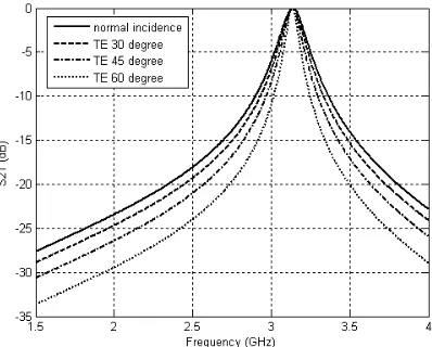
lumped capacitors at this frequency band is larger by a factor of about four in comparison with the structure shown in Fig. 1, but also a conventional notch square ring FSS is transparent at some higher order resonance frequencies near the dominant resonance frequency that is not favourable. Furthermore, the maximum resonance frequency shift for different incidence angles for this structure is much less than the resonance frequency shift of a conventional FSS with notch square ring.
Figure 1. The Geometry of notch square ring FSS with ceramic chip capacitors. (T y,T z,L,W) = (10,10,6,2) mm.
Figure 3. Transmission coefficient of the FSS structure shown in Fig. 1 for normal incidence.
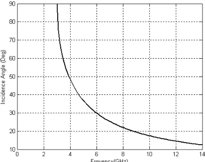
Figure 4. The incidence angle of the corresponding plane wave versus frequency for the dominant mode of the waveguide shown in Fig. 5.
Figure 5. Setup of the filter within the waveguide. (a = 50 mm,
b= 10 mm).
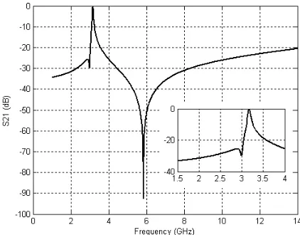
Figure 6. Transmission coefficient for the dominant mode of the waveguide filter shown in Fig. 5.
the same as the waveguide shown in Fig. 5 because of the waveguide cut-off frequency considerations. Therefore, the waveguide dimension in one direction is reduced considerably and undesirable higher order resonance frequencies near the dominant resonance frequency are eliminated by using lumped capacitors in the FSS structure. The filter bandwidth is less than 2%. Therefore, it is suitable for narrow band applications.
4. CONCLUSION
A new band-pass FSS structure with lumped capacitors suitable for the design of the waveguide filters has been presented. By using lumped capacitors, the waveguide filter dimension is reduced about 80% in one direction compared with the analogous waveguide filter without lumped capacitors. Furthermore several undesirable higher order resonance frequencies near the dominant resonance frequency are eliminated. The future work is designing wideband waveguide filters by using multiple FSSs placed on the transverse plane of the rectangular waveguide.
REFERENCES
1. Konishi, Y. and K. Uenakada, “The design of a bandpass filter with inductive strip-planar circuit mounted in waveguide,” IEEE Trans on Microwave Theory and Tech., Vol. 22, No. 9, 839–841, September 1974.
2. Vahldieck, R. and W. J. R. Hoefer, “Finline and metal insert filters with improved passband separation and increased stop-band attenuation,”IEEE Trans. on Microwave Theory and Tech., Vol. 33, No. 12, 1333–1339, December 1985.
3. Robinson, A. J., R. D. Seager, and J. C. Vardaxoglou, “Waveguide with resonant array inserts,” Electron. Letter, Vol. 28, No. 23, November 1992.
4. Langley, R. J., “A dual-frequency band waveguide using FSS,”
IEEE Microwave Guided Wave Letter, Vol. 3, No. 1, 9–10, January 1993.
5. Lockyer, D. S. and J. C. Vardaxoglou, “Reconfigurable FSS response from two layers of slotted dipole arrays,”Electron. Letter, Vol. 32, No. 6, March 1996.
applica-tions,” IEEE Microwave Wireless Components Letter, Vol. 11, No. 3, 112–114, March 2001.
7. Monorchio, A., G. Manara, U. Serra, G. Marola, and E. Pagana, “Design of waveguide filters by using genetically optimized frequency selective surfaces,” IEEE Microwave and Wireless Component Letters, Vol. 15, No. 6, 407–409, June 2005.
8. Martynyuk, A. E., J. Lopez, and N. A. Martynyuk, “Active frequency selective surfaces based on loaded ring slot resonators,”
Electronic Letters, Vol. 41, No. 1, 2005.
9. Roden, J. A., S. D. Jedney, M. P. Kesler, J. G. Maloney, and P. H. Harms, “Time-domain analysis of periodic structures at oblique incidence: Orthogonal and non-orthogonal FDTD implementations,” IEEE Trans. Microwave Theory and Tech., Vol. 46, 420–427, 1998.
10. Picket-May, M. J., A. Taflove, and J. Baron, “FDTD modelling of digital signal propagation in 3D circuits with passive and active loads,”IEEE Trans. Microwave Theory and Tech., Vol. 42, 1514– 1523, 1994.