Design and Simulation of an Improved Energy Selective Surface
Bo Yi*, Yanfei Dong, Cheng Yang, Peiguo Liu, and Yan Li
Abstract—Energy selective surface (ESS) proposed in recent years is one of the most effective means for defending high intensity electromagnetic wave attacking. This paper presents an improved ESS structure and its systematic design method. An ESS prototype is designed and fabricated based on a given requirement. Its insertion loss is measured in an anechoic chamber, and its shielding effectiveness is tested under HPM and UWB irradiation. Measured results show that the ESS sample meets the given requirement.
1. INTRODUCTION
During past decades, high power electromagnetic sources and wideband technologies have achieved notable progress and electromagnetic weapons become assessable to offenders [1, 2]. Electromagnetic weapons can be as small as a suitcase and carried into a building with public access [3]. They can irradiate high intensity electromagnetic wave: high power microwave (HPM) and ultra-wideband source (UWB), both with an intensity about 10 kV/m at target place (dependence on range) and pose a serious threaten to most information equipments [4]. The most effective way to protect information equipments is to put them in shielding room [5]. But this method cannot be applied to facilities needed to interact with outer environment. Aiming at protecting these facilities, many protection methods, like carbon foam, manganite films and frequency selective surface (FSS), are proposed [6, 7]. Usually, high intensity electromagnetic wave may couple in electronic and electrical systems through ”Front door” such as antennas and “back door” such as cables, apertures [8, 9]. Among them, antenna provides an important channel for high intensity electromagnetic wave entering information systems. FSS as a protecting method has been studied for many decades [10]. But it will fail to provide protection when the frequency of high intensity electromagnetic wave is located within its passband. In order to overcome this defect, limiting FSS was designed in [11, 12]. It can change its passband when high intensity electromagnetic wave arrives. Scott et al. adopted FSS loaded phase change material to realize adaptive protection [13]. At a given temperature, the resistivity of phase change material decreases abruptly, typically by three orders of magnitude. But some time is needed for temperature of phase change material increasing and reaching the threshold; therefore, some part of the energy may leak into receiver front end. Plasma limiter is another method of adaptive protection against high electromagnetic waves [14].
The concept of energy selective surface (ESS) as a new self-actuated protection method has been proposed in [5]. Compared with the adaptive protection methods mentioned above, ESS pays more attention to amplitude of incident wave instead of frequency. In other words, ESS can realize ultra wideband defending. Using proper diodes as the switchable device, the response time of ESS only needs several nanoseconds under UWB irradiation and within 100 ns under HPM irradiation.
The ESS structure in [5] validates the concept of energy selection. This paper improves the structure of ESS and presents systematic design method for it as well. Compared with the energy selective
Received 20 September 2015, Accepted 9 November 2015, Scheduled 30 November 2015 * Corresponding author: Bo Yi (yibo [email protected]).
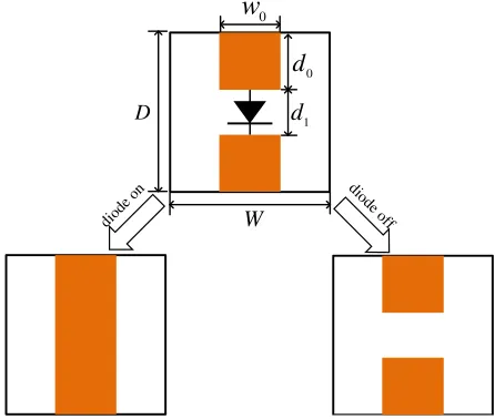
In this section, energy selective mechanism is firstly introduced. This mechanism implies that ESS is transparent to low intensity electromagnetic wave while shielding high intensity one in working band [7]. In order to realize energy selective mechanism, ESS needs a variable impedance surface. PIN diode is one of the good choices as a nonlinear device mounted on the metal unit cell to achieve variable impedance surface. A conductor cross patch usually has a higher resonant frequency than a loop patch with same period [15]. So the conductor cross patch is more suitable for constructing ESS. The property of diode loaded conductor cross patch with arbitrary polarization direction can be estimated by studying the rectangle patch with diode loaded only valid for an incident wave at a specific polarization direction [16]. So the unit cell of ESS can be simplified to the structure shown in Figure 1. Here,Dand W represent the length and width of ESS unit cell, respectively. w0 denotes the width of metallic patch. d0 and d1 represent the length of metallic patch and width of slot between adjacent metallic patches, respectively. Figure 1 also presents equivalent metal structure of ESS unit cell when diode is on and off.
0
w
1 d
0 d
diode
on diode of
f
D
W
Figure 1. The unit cell of ESS and its equivalent circuit when diode on or off.
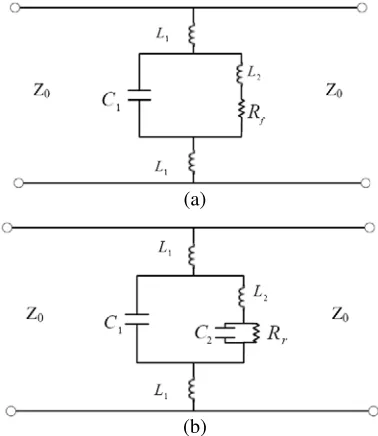
The equivalent circuits of ESS unit cell in Figure 1 are shown in Figure 2. PIN diode is replaced by its reverse and forward bias equivalent circuit model, and metal patch is replaced by inductor [17]. The slot between adjacent metallic patches is equivalent to a capacitor.
In Figure 2, C1 and L1 represent the equivalent capacitance and inductance of metallic strips, respectively. Z0 and L2 denote the characteristic impedance of space and package inductance of PIN diode, respectively. In Figure 2(a), Rf represents the equivalent forward resistance when PIN diode is on. In Figure 2(b), C2 and Rr denote the equivalent package capacitance and reverse resistance, respectively, when PIN diode is off. L2, Rf, C2 and Rr can be estimated based on the measured S parameters.
When the electric field polarization is parallel to the metallic edges, the metallic strips are inductive and can be replaced by inductor. We can also estimate the equivalent inductance Lper unit length as follows [18].
L = μ0d
2π
In csc
πw
2W
+Gx
(a)
(b)
Figure 2. Equivalent circuit of ESS unit cell. (a) Equivalent circuit of ESS when PIN diode is on. (b) Equivalent circuit of ESS when PIN diode is off.
Gx = 12
1−βx22
2Ax
1−β 2 x 4
+ 4A2xβ2x
1−β 2 x
4 + 2Axβ 2 x
1 + β 2 x 2 −
β4x
8
+ 2A2xβx6
(2)
Ax = 1
1−
W
λ
2 −1 (3)
βx = sin2πwW (4)
where, w andW denote the width of metal strip and unit cell, respectively.
When the electric field polarization is perpendicular to the metallic edges, the metallic strips are capacitive and can be replaced as capacitor. We can also estimate the equivalent capacitance C per unit width as follows.
C = 2ξ0wD
πW
In csc
πd 2D
+Gb
(5)
Gb = 1
2
(1−βb2)2
2Ab
1−β 2 b 4
+ 4A2bβb2
1− β 2 b
4 + 2Abβ 2 b
1 +β 2 b 2 −
βb4
8
+ 2A2bβb6
(6)
Ab = 1
1−
D
λ
2 −1 (7)
βb = sin2πd
D (8)
3. SIMULATION AND DESIGN OF IMPROVED ESS 3.1. Structural Parameters Analysis
In order to design a proper ESS, we first study the influence of each structural parameter to its performance through simulation in CST MWS.
Select the parameters in Table 1 to construct ESS and keep them unchange unless special declaring. Rogers RO4350 was chosen as substrate material, and its thickness was set to 0.5 mm. In simulation, diode was replaced by capacitor and inductor in series at zero bias and by resistor and inductor in series at forward bias. Some useful results can be obtained by undertaking simulation with different conditions [7]. In order to decrease starting threshold, PIN was mounted on the place where electric field was maximal.
Table 1. Geometrical parameters list for ESS.
Parameter Dimensions (mm)
W 6
D 6
w0 5.5
d0 2.6
d1 0.8
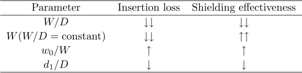
Table 2 summarized the relationship between structural size and transmission characteristic based on simulation and calculation results based on the equivalent circuit.
Table 2. The relationship between structural size and transmission characteristic. Parameter Insertion loss Shielding effectiveness
W/D ↓↓ ↓↓
W(W/D= constant) ↓↓ ↑↑
w0/W ↑ ↑
d1/D ↓ ↓
In Table 2, symbols↑↑and↑ represent that the parameter is positively related to the performance of ESS. Symbols ↓↓ and ↓ represent that the parameter is negatively related to the performance. ↑↑ and ↓↓ indicate that the parameter has great impact on ESS performance. ↑ and ↓ indicate that the parameter has moderate impact on ESS performance.
In order to reduce insertion loss, rectangular patch can be replaced by the patch shown in Figure 3. The improved patches increase the gap between adjacent patches and reduce the equivalent capacitance of metal patches essentially. In other words, the ESS based on improved shape has a lower insertion loss than the ESS based on rectangular shape.
1
w
2 d 0
d
1
d
0 w
Figure 3. Improved metal patch shape.
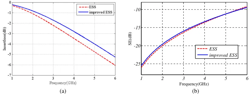
Figure 4 shows the comparison of transmission performance between ESS and improved ESS. As shown in Figure 4(a), the improved ESS has a lower insertion loss than the ESS. Meanwhile, the shielding effectiveness of improved ESS almost keeps the same.
1 2 3 4 5 6
-25 -20 -15 -10
Frequency(GHz)
SE
(d
B
)
ESS improved ESS
(a) (b)
Figure 4. Comparison of transmission performance between ESS and improved ESS. (a) Comparison of insertion loss between ESS and improved ESS. (b) Comparison of shielding effectiveness between ESS and improved ESS.
3.2. Example of Designing Improved ESS
Based on the conclusions above, an ESS was fabricated, and the requirement of it is shown in Table 3.
Table 3. The given protection requirement of ESS.
defending
frequency Insertion loss
Shielding effectiveness
voltage of bap6302 PIN diode is about 5 V at 1.5 GHz. So the period size should be bigger than 5 mm. Based on the consideration above, the size of period was set to 6 mm. The value of parameters in Table 1 can be used to construct the ESS based on the above discussion. Considering the size of PIN diode and convenience to solder it, w1 was set to 0.8 mm andd2 set to 0.5 mm.
In order to study the influence of ESS on antenna pattern, a horn loaded with an improved ESS at its aperture was simulated in CST MWS. Figure 5 shows the comparison of the field patterns of horn antenna directional diagram between mounted and unmounted ESS. We find that ESS only slightly changes the side lobe of the horn antenna and has little influence on its main lobe at both E and H planes.
30
210
60
240
90 270
120 300
150 180 0
with ESS without ESS
330 30
210 60
240
90 270
120
300
150
330
180 0
with ESS without ESS
(a) (b)
Figure 5. The compare between horn antenna’s directional diagram with and without ESS. (a)H-plane directional diagram. (b)E-plane directional diagram.
Figure 6 shows the transmission characteristic when diodes is on and off at different incident angles. When incident angle is less than 30◦, transmission characteristic of ESS almost keeps stable. But as incident angle goes on increasing, shieling effectiveness and insertion loss also begin to increase rapidly.
4. EXPERIMENT RESULT AND DISCUSSION
An ESS prototype based on the improved structure was fabricated using printed circuit board technology. The ESS sample consisted of 50×50 unit cells. The substrate material was Rogers RO4350. Around the ESS unit cell, there was a metal strip with width of 10 mm at each side. The overall size of ESS prototype was about 400 mm ×400 mm. The measurement for ESS was divided into three steps. The first step was to measure insertion loss in an anechoic chamber. The second and third ones were to measure shielding effectiveness under the irradiation by HPM and UWB in outer space.
The test schematic for insertion loss was set as in Figure 7. Two ridged horns were used as transmitter antenna and receiver antenna, respectively. An absorbing wall was placed between transmitting and receiving antennas. They were put at two sides of the absorbing wall with equal distance which was about 0.7 m to insure ESS located in the far-field region. An Anritsu vector network analyzer was employed to measure the S parameters. The measured and simulated results are shown in Figure 8.
0 1 2 3 4 5 6
x 109
-12 -10 -8 -6 -4 -2 0 Frequency(Hz) In se rt io n L o ss (d B ) Theta=0 Theta=15 Theta=30 Theta=45 Theta=60
0 1 2 3 4 5 6
x 109
-35 -30 -25 -20 -15 -10 -5 Frequency(Hz) S hie ld in g E ff ec ti v en es s( d B ) Theta=0 Theta=15 Theta=30 Theta=45 Theta=60 (a) (b)
Figure 6. Transmission characteristic of ESS under different incident angle. (a) Insertion loss of ESS under different incident angle. (b) Shielding effectiveness of ESS under different incident angle.
Figure 7. Experiment setup for measuring insertion loss of ESS.
1 2 3 4 5 6
x 109 -10 -9 -8 -7 -6 -5 -4 -3 -2 -1 0 1 2 Frequency(Hz) In se rt io n L o ss (d B ) simulated result measured result
Figure 8. Simulation result in CST compared to measured result.
Figure 9. Measurement setup for shielding effectiveness of ESS under irradiating by HPM.
because of the switching time of PIN diodes. After PIN diode switches on, the amplitude of limiting field is about 250 V/m which is significantly reduced compared with the field without ESS. The size of period and the type of PIN diode are two factors influencing intensity of limiting field. The smaller the period size is, the smaller the intensity of limiting field is. To choose PIN diode with low equivalent resistance and inductance decreases the amplitude of limiting field. Another method to decrease limiting field is to add a bias voltage on diode.
Figure 12 shows the shielding effectiveness of improved ESS under irradiating with different amplitude of electric field. When the electric field around improved ESS is low, it can pass improved ESS with low attenuation. As the intensity of radiation field increases, the shielding effectiveness also
-2 -1 0 1 2
x 10-6 -2000 -1500 -1000 -500 0 500 1000 1500 2000 Time(s) E lec tr ic I n te rs it y( V /m ) 1500V/m 1180V/m 780V/m
Figure 10. Free space field intensity around parabolic antenna with different transmitting amplitude.
-2 -1 0 1 2
x 10-6 -1000 -800 -600 -400 -200 0 200 400 600 800 1000 Time(s) E lectr ic I n te ns ity (V /m ) 250V/m 250V/m 250V/m
Figure 11. Electric field intensity after passing ESS with different transmitting amplitude.
0 500 1000 1500 2000 2500 3000 3500 4000 4500 5000 4 6 8 10 12 14 16 18 20
Electric Field Intensity(V/m)
S hiel di ng E ff ect iv en ess( d B )
Figure 12. Shielding effectiveness of ESS as a function of radiation field intensity.
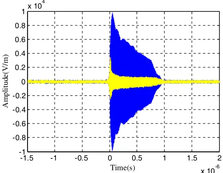
-1.5 -1 -0.5 0 0.5 1 1.5 2
x 10-6 -1 -0.8 -0.6 -0.4 -0.2 0 0.2 0.4 0.6 0.8
1x 10
4 Time(s) Am p litu de (V /m)
increases keeping limiting field stable until it reaches about 19 dB. It is because diode reaches saturation. If the intensity of radiation field goes on increasing, the amplitude of limiting field also increases. As shown in Figure 13, when the amplitude of radiation field is about 6000 V/m, the amplitude of limiting field is about 600 V/m.
Figure 14 shows the measurement setup for shielding effectiveness under UWB irradiation. A UWB source was used to produce high power UWB irradiation electromagnetic wave. The other measurement setup was the same as measurement setup under HPM irradiation.
Figure 14. Measurement setup for shielding effectiveness of ESS under irradiating by UWB.
0 1 2 3
x 10-8 -2000
-1500 -1000 -500 0 500 1000 1500 2000 2500
Time(s)
A
m
p
litud
e(
V
)
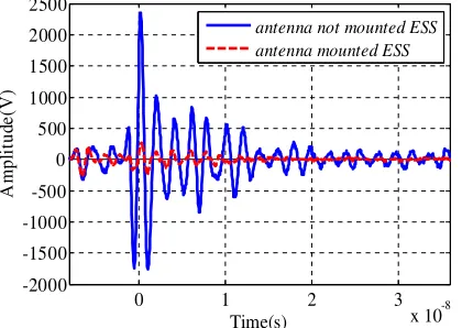
antenna not mounted ESS antenna mounted ESS
Figure 15. Comparing of electric field intensity with receiver mounted ESS or not.
As shown in Figure 15, when ESS is mounted on receiving antenna, the electric field intensity passing through ESS decreases sharply. The shielding effectiveness reaches 19.5 dB. The ripple disappears after about 10 ns which is different from the origin waveform. The reason is that diode recovering from conducting needs some time. From Figure 15, we know that ESS can be effective to defend UWB attacking with short rising time and strong intensity.
Comparing Figure 11 and Figure 15, we can find that the ESS response time irradiated by UWB is shorter than that irradiated by the HPM. The reason is that the frequency, amplitude and rising edge of the incident waves have a great influence on the response time of the ESS, where a lower frequency, higher amplitude and sharper rising edge may result in a shorter response time of ESS.
5. CONCLUSION
In this paper, an improved ESS is presented, and its systematic design method is introduced. The improved ESS decreases the insertion loss and expands working band. Through CST simulation, we find that the improved ESS has little influence on the antenna pattern. An improved ESS prototype is fabricated using printed circuit board technology. The experiment results show that the insertion loss is less than 1 dB below 1.8 GHz and that the maximum shielding effectiveness reaches 19 dB at measurement frequency under HPM irradiation, which is consistent with simulation result. UWB irradiation testing proves that the improved ESS can be applied to defend UWB attacking, and the shielding effectiveness reaches 19.5 dB.
ACKNOWLEDGMENT
The authors would like to thank Dr. Ding Liang for his help with our paper writing.
REFERENCES
Vol. 46, 396–403, 2004.
5. Yang, C., P. Liu, and X. Huang, “A novel method of energy selective surface for adaptive hpm/emp protection,” Antennas and Wireless Propagation Letters, Vol. 12, 112–115, 2013.
6. Zurauskiene, N., S. Balevicius, and L. Zurauskiene, “Nanostructured manganite films as protectors against fast electromagnetic pulses,” IEEE Transactions on Plasma Science, Vol. 41, 2890–2895, 2013.
7. Tan, J., P. Liu, C. Yang, et al., “EM simulation analysis of the Energy Selective surface,” High Voltage Engineering, Vol. 39, 30897–30903, 2013.
8. Nilsson, T., “Investigation of limiters for HPM and UWB front-door protection,” Ph.D. Dissertation, Link¨oping University, 2006.
9. Lee, K.-A. and K.-C. Ko, “Propagation model of high power electromagnetic pulse by using a serial-parallel resistors circuit,” IEEE Transactions on Plasma Science, Vol. 42, 3309–3312, 2014. 10. Bolioli, S. and J. C. Joly, “Front-door protection using frequency selective surface,” International
Symposium on Electromagnetic Compatibility (EMC), 1–4, Athens, 2009.
11. Monni, S., D. Bekers, M. van Wanum, et al., “Limiting frequency selective surface,” EuMC 2009 Microwave Conference, 606–609, Rome European, 2009.
12. Monni, S., D. J. Bekers, M. van Wanum, et al., “Protection of RF electronics using tuneable frequency selective surfaces,” 3rd European Conference on Antennas and Propagation, EuCAP 2009, 3170–3174, Berlin, 2009.
13. Scott, S., C. D. Nordquist, M. J. Cich, et al., “A frequency selective surface with integrated limiter for receiver protection,”Antennas and Propagation Society International Symposium (APSURSI), 1–2, Chicago, 2012.
14. Yang, G., J. Tan, D. Sheng, et al., “Plasma limiter for Protecting against high power microwave,”
Journal Of Scientific & Industrial Research, Vol. 67, 685–687, 2008.
15. Munk, B. A.,Frequency Selective Surface: Theory and Design, Wiley, New York, 2000.
16. Zhang, Y., M. Yuan, and Q. Liu, “ Wide band response of an electromagnetic wave shield based on a diode grid,” Progress In Electromagnetic Research, Vol. 141, 591–606, 2013.
17. Chang, K., I. K. Sang, J. Y. Young, “Equivalent circuit modeling of active frequency selective surface,” IEEE on Radio and Wireless Symposium, 663–666, Orlando, 2008.
18. Marcuvitz, N.,Waveguide Handbook, 280–291, McGraw-Hill, London, UK, 1951.