Available online: https://edupediapublications.org/journals/index.php/IJR/ P a g e | 51
A Novel Coupled-Inductor Single-Phase Boost DC-AC Inverter for
Photovoltaic Systems
Tanakanti Adi Seshudu
1, D. Masthan
21PG Scholar, Dept. of EEE, Dr.K.V. Subba Reddy Institute of Technology, Kurnool, A.P.
2Assistant Professor, Dept. of EEE, Dr.K.V. Subba Reddy Institute of Technology, Kurnool, A.P.
ABSTRACT: This paper presents a new single-phase switched coupled-inductor dc–ac inverter featuring higher voltage gain than the existing single-phase qZ-source and semi-Z-source inverters. Similar to the single-phase qZ-source and semi-Z-source inverters, the proposed inverter also has common grounds between the dc input and ac output voltages, which is beneficial especially for photovoltaic inverter systems. The inverter volume and maximum current flowing can be reduced significantly through the coupling of all inductors. A theoretical analysis of the proposed inverter is described and a 280-W experimental prototype is built to verify the performance of the inverter.
Index Terms—Common ground, dc–ac inverter,
high voltage gain, qZ-source inverter, single-phase inverter, switched-coupled- inductor (SCL), Z-source inverter.
I. INTRODUCTION
Now-a-Days, there is an increasing demand for low-cost single-phase dc–ac inverters in many applications such as photovoltaic (PV), fuel cell, and battery powered systems. The conventional methods are shown in Fig.1. 1. Fig.1. 1(a) shows the well-known full-bridge (FB) inverter referred to as buck inverter in this project. In this circuit, the inverter output voltage (vo) cannot be greater than input voltage (Vin). When the input voltage is
low, a boost dc–dc converter is inserted between
Available online: https://edupediapublications.org/journals/index.php/IJR/ P a g e | 52
Fig. 1 Conventional single-phase inverters. (a) FB inverter. (b) FB inverter with dc–dc boost converter
Vo/Vin=(2D − 1D)/D (1)
In (1), D is defined as the duty ratio of switch S2 .As shown in Fig.1, the two topologies share common grounds between Vin and vo, and thus they can minimize the possible ground leakage current problem effectively when they are used for PV inverter. However, as depicted in Fig1(c), their attainable maximum voltage gain is limited to 1, which means that they are not suitable for applications where input voltage is low. In order to overcome the limitations of Fig.1 while maintaining the doubly ground features, a three-switch three-state single-phase Z-source inverter (TSTS-ZSI) was introduced in. Fig.2 shows the boost-based TSTS-ZSI and buck-boost based TSTS-ZSI, respectively. The inverters can have higher voltage gain than 1, and they comprise three switches, three capacitors, and three inductors. Although higher voltage gain is obtained, the three inductors (L1, L2, and L3) in the TSTS-ZSI make the circuit a bit bulky and heavy. In addition, the switch signals of the inverter are all different and relatively complicated.
Fig.2. Single-phase qZ-source inverters. (a) Single-phase CF-qZ-source inverter. (b) Semi-qZ-source inverter. (c) Voltage gain.
Although higher voltage gain is obtained, the three inductors (L1,L2, and L3) in the TSTS-ZSI make the circuit a bit bulky and heavy. In addition, the switch signals of the inverter are all different and relatively complicated.
In this paper, a single-phase switched-coupled-inductor dc– ac inverter is proposed. Similar to the TSTS-ZSIs, the proposed inverter can obtain higher voltage gain than the circuits in Fig. 2 and maintains same ground between Vin and vo. The
Available online: https://edupediapublications.org/journals/index.php/IJR/ P a g e | 53 be coupled together, which will lead to more
compact and cost effective solution than the TSTS-ZSI. In addition, the switch signal generation is relatively simpler than the TSTS-ZSI. A 280-W prototype inverter is built and its performances are verified through experiment.
II. RELATED WORK
A conventional HVDC system uses an ac line frequency (50/60 Hz) transformer to boost the voltage and ac/dc converters for rectification and power flow control. This technology is robust and reliable, but it causes a considerable increase in weight and volume, which leads to higher installation cost. A high-power density can be obtained by replacing the bulky 50/60-Hz transformers with high-frequency transformers. Unfortunately, high-frequency transformers with large turn ratios are difficult to design at high voltages and mega power levels because of the enormous expense of the magnetic material, core, and dialectic losses. One of the key-enabling components for HVDC is the high power dc/dc conversion system because it has a rigid structure, is easy to control system and more compact. To overcome the increasing power losses and maintain a high power density, it is expected that large marine turbines will require a higher voltage with high-voltage gain dc/dc conversion systems to interface with the power transmission networks. Single-module dc/dc boost converters can theoretically achieve infinite voltage conversion ratios but practically, the maximum gain is limited by circuit imperfections, such as parasitic elements and switch commutation times. Multiple module boost converters have been proposed to achieve high conversion ratios for applications to offshore wind farms. Nevertheless, because the duty ratio of
the main switch is large to achieve high-voltage gain, the switching frequency is relatively low to reduce the losses and also allows sufficient turn-off time for the switches.
2.1 PROBLEM FORMULATION
Available online: https://edupediapublications.org/journals/index.php/IJR/ P a g e | 54
systems. The proposed converter combines the output of two modular cells to reduce the device count, output capacitance requirements, and total capacitor power rating. The principle of a soft-switching operation and output voltage analysis of the proposed converter are described in detail. The output capacitors are charged and discharged continuously by a 180◦ phase shift with respect to each other to eliminate the output voltage ripples without adding extra component.
2.2 OBJECTIVE OF THE THESIS
In this thesis, a single-phase switched-coupled-inductor dc–ac inverter is proposed. Similar to the TSTS-ZSIs, the proposed inverter can obtain higher voltage gain than the circuits in Fig. 2 and maintains same ground between Vin and
vo. The proposed inverter also requires three active switches, but all the inductors in the circuit can be coupled together, which will lead to more compact and cost effective solution than the TSTS-ZSI. In addition, the switch signal generation is relatively simpler than the TSTS-ZSI. A 280-W prototype inverter is built and the performance of the proposed method is evaluated through simulations in MATLAB/SIMULINK environment.
III. PROPOSED SYSTEM
The proposed inverter and it takes similar structure with the single-phase CF-qZ-inverter shown in Fig.3. Compared with Fig.2, the proposed inverter has an additional switch (Sx), capacitor (Cx), and inductor (L2) coupled with inductor L1. The inductors L1 and L2 are coupled with 1: n turn’s ratio and all the inductors in the proposed topology can be coupled altogether as will be discussed in Section III. The added 1: n coupled inductor contributes to the increase of voltage gain. Although the leakage inductance of
the coupled inductor may induce a voltage spike across switch S1, this is not a major problem because such a voltage spike and the voltage of S1 are low. In Section III, it will be found that the voltage stress of S1 is always half of S2 or Sx if leakage inductance is not considered. Therefore, as long as the voltage overshoot caused by the leakage inductance is not so high, the voltage stress of S1 will be less than that of S2 and there is not much problem in selecting switching device for S1. On the other hand, the leakage inductance is beneficial in limiting the current passing through Cx. Switches S1 and S2 are complementary as in the single-phase qZ-source inverter and the switch Sx is synchronized with S1. A. Mode Analysis of the Proposed Inverter Fig.4.2 shows operation of the proposed inverter and there are two operational modes during one switching cycle. In mode 1, switches S1 and Sx are turned-on, and S2 is turned-OFF. In mode 2, switches S1 and Sx are turned-OFF, and S2 is turned-on. Followings are the detailed mode analysis of the proposed inverter. In mode 1, the capacitor Cx is charged to (n + 1) Vin. Since the Cx is being charged and discharged during one switching period, its voltage has ripple and the ripple voltage depends on the output power. Therefore, when the voltage difference between (n + 1)Vin and Cx is high, relatively high surge (charging) current will flow through Vin − Dx (Sx ) − L2 − Cx − S1 and the switching devices in this path (Sx and S1 ) can be damaged. In order to limit the high surge current, a current limiting inductor is necessary.
Available online: https://edupediapublications.org/journals/index.php/IJR/ P a g e | 55 Fig 3 Proposed dc–ac inverter
Fig. 4 Mode analysis of the proposed inverter. (a) Mode 1: S1 and Sx are ON, and S2 is OFF. (b) Mode 2: S1 and Sx are OFF, and S2 is ON.
In mode 2, capacitor Cx is discharged by the inductor current, iL1. From Fig. 4(b), the voltage and current relations in mode 2 are derived as follows:
In mode 2, capacitor Cx is discharged by the inductor current, iL1. From Fig. 4(b), the voltage and current relations in mode 2 are derived as follows:
Fig. 5 Voltage gain comparison
Available online: https://edupediapublications.org/journals/index.php/IJR/ P a g e | 56
From the flux (volt–second) balance condition on L3, the capacitor C2 voltage is derived as follows:
Where D is the duty cycle of switch S2. By using (7)–(9), the voltage gain of the proposed inverter is derived as follows:
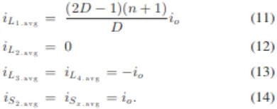
Fig. 5 shows the voltage gain of the proposed inverter when n = 1 and compared with the conventional inverters shown in Fig.2(c). It is found that the proposed inverter has a higher voltage gain than the conventional inverters shown in Figs. 1(a) and 2. According to the charge balance condition on Cx , C1 , and C2 , the inductor currents averaged in one switching period are derived as follows:
Currents of inductors L1 and L2 are different in respective mode unlike inductor currents iL3 and iL4 . In mode 1, where current ripple is ignored, they are derived
In mode 2, they are expressed as follows:
Fig. 6. Gate signal generation of the proposed inverter.
Fig. 7. Circuit topology of the proposed inverter when all inductors are coupled into one
core
Available online: https://edupediapublications.org/journals/index.php/IJR/ P a g e | 57
(18), modulation index (M) of the inverter is derived as follows:
By substituting (18) and (19) into (10), the following duty cycle equation is derived as follows:
When n = 1 and M = 3, the duty cycle range of the proposed inverter is 0.25–1.0. Fig.6 represents the gate signal generation of the proposed inverter. When reference signal (vref) is greater than the carrier signal (vc ), switch S2 is turned on and switch S1 is turned OFF.
4.2 MAGNETIC INTEGRATION OF
INDUCTORS AND COMPARISON
A. Magnetic Integration of Inductors As discussed in Section II, the L1 and L2 are coupled with 1: n ratio to obtain higher voltage gain. In this section, it is revealed that all the four inductors (L1, L2, L3, and L4) in the proposed inverter can be coupled using one magnetic core.
Table: 1 Device stress of the proposed inverter
The previous analysis shows that the voltages across each inductor during mode 1 are as follows:
Similarly, the voltages across each inductor during mode 2 are as follows:
From (21) and (22), it is found that regardless of the operating mode, the four inductors in the proposed inverter have the following voltage relationships:
Therefore, all the inductors can be coupled using one core, which leads to significant reduction in magnetic volume and converter size. It should be noted that n is the turns ratio and it is not the real number of turns. Fig.7 shows the final completed circuit of the proposed inverter with the inductor polarity dots marked. The operation with magnetic integration is the same as that of the previous analysis in Section II.
Available online: https://edupediapublications.org/journals/index.php/IJR/ P a g e | 58
proposed inverter when n = 1 with the boost based TSTS-ZSI shown in. k is maximum of modulation index. Although the buck–boost-based TSTS-ZSI has lower device stresses, it has drawbacks like more complicated gate signal generation, discontinuous input and output current, and requires additional LC filter that builds the circuit structure more complex and large inductor. For these reasons, the boost-based TSTS-ZSI is compared with the proposed inverter. From the result of Table
II, it is evident that the overall voltage and current stresses of the proposed inverter are greater than those of the TSTS-ZSI and the proposed inverter requires one more capacitor. However, current stress of the proposed inverter is lower than that of the boost-based TSTS-ZSI when M is lower than 2.4. Moreover, the proposed inverter can reduce the magnetic volume through the coupling of all separate inductors
Table: 2. Comparison of inverters
Comparison of maximum current ripple, average current, and maximum capacitor voltage is summarized in Table II. According to the Table II, when compared with the boost-based TSTS-ZSI, the inductor current ripples of the proposed inverter are reduced by more than 2 due to
Available online: https://edupediapublications.org/journals/index.php/IJR/ P a g e | 59
assumed that L1 and L2 are equal. Although, the C2 capacitor voltage of the proposed inverter is greater than that of the boost-based TSTS-ZSI, the capacitor voltages of Cx and C1 in the proposed converter are lower than those of the boost-based TSTS-ZSI. Moreover, inductor has more influence on size and weight than capacitor. The average inductor currents of the proposed inverter and boost-based TSTZ-ZSI in one switching period are almost the same. In conclusion, the proposed inverter can reduce overall magnetic volume because lower inductance is required. In addition, the boost-based TSTS-ZSI should have large output capacitor because of discontinuous output current. Moreover, the gate signal generation of the proposed inverter is much simpler than that of the TSTS-ZSI.
TABLE III
ELECTRICAL SPECIFICATIONS OF THE
PROPOSED INVERTER
Output power 280 W
Input voltage 62 Vdc
Output voltage 110 Vrms / 60
Hz
Switching frequency 20 kHz
IGBT (Sx, S1 , S2 ) FGH40N60
Coupled inductor
Core EE7066 Inductance (L 1 , L 2 ) 60 uH
Inductance (L 3 , L 4 ) 240 uH
Capacitance (Cx, C 1 ) 100 uF
Capacitance (Co) 4.4 uF
Table: 3. Electrical specifications of the proposed inverter
IV. SIMULATION RESULTS
Simulation results proposed a New single- Phase Switched- coupled- Inductor DC-AC Inverter for
Photovoltaic Systems. The simulated system is shown in fig.5.1. Simulation studies are carried out in the MATLAB/SIMULINK environment.
Available online: https://edupediapublications.org/journals/index.php/IJR/ P a g e | 60 Fig 8: Block diagram for proposed methodology
SIMULATION RESULT ANALYSIS
A 280-W prototype inverter is built and tested. Detailedelectrical specifications of the proposed inverter are summarized in Table III. As already mentioned in Section II, a relatively small current limiting inductor is required in the path Vin −Dx (Sx) − L2 −Cx −S1 to limit the high surge current. In the proposed circuit, the leakage inductance (about 300 nH) generated by coupling of L1 and L2 is used for this purpose. Followings are the experimental waveforms of the proposed inverter when Vin = 62 V,M= 2.5, and Po = 280 W. Fig.9 shows the experimental wave form of the output voltage and the capacitor C2 voltage. Figs.
9 and 10 show the voltages across all switches (VSx, VS1, and VS2). As expected, there is voltage overshoot in switch S1 caused by the leakage inductance and there are no noticeable overshoots in the switches S2 voltage varying with D, the voltages across C1 and Cx are almost constant and they are fixed to 3Vin and 2Vin, respectively. Figs. 5.5 and 5.6 show current waveforms. Shows the efficiency of the proposed inverter tested with Vin = 62V with output power varies.
(a) Output voltage V0
(b) Output Voltage Vc2
Fig 9: Simulink waveforms of the proposed inverter (Vc2, V0)
Available online: https://edupediapublications.org/journals/index.php/IJR/ P a g e | 61 (b) Output Voltage Vs1
Fig 10 : Simulink waveforms of the proposed inverter (Vs2, Vs1)
(a) Output Voltage Vc1
(b) Output Voltage Vc1
(c) Output Voltage(Vs2)
Fig 11: Simulink waveforms of the proposed inverter (Vc1, Vc1, Vs2)
(a)Output Current Is1
(b) Output Current Isx
Fig 12: Simulink waveforms of the proposed inverter current waveforms (Is1, Isx)
(a) Output Current Isx
(a) Output Current Is2
Available online: https://edupediapublications.org/journals/index.php/IJR/ P a g e | 62 Input DC waveforms
Output Voltage (Vg)
Fig 14: Simulink waveforms of the proposed inverter (Input DC waveform, Output Voltage (Vg))
V. CONCLUSIONS
In this project, the single-phase switched coupled inductor dc– ac inverter was presented. It has an operation principle similar to that of a single-phase qZ-source inverter. With the addition of components Sx, Cx, and the coupled inductor, voltage gain of the proposed inverter can be extended to greater than 2. The magnetic integration of all inductors decreases the converter volume significantly and the proposed inverter has relatively simple gate signal generation. Moreover, similar to the single-phase qz- source inverter and the TSTS-ZSI, the proposed inverter shares common grounds between the dc input and the ac output voltage. A 280-W prototype inverter was built and tested to verify operation of the proposed inverter.
VI. REFERENCES
[1]T. Kawabata, K. Honjo, N. Sashida, K.
Sanada, and M. Koyama, “High- frequency
link dc/ac converter with PWM
cycloconverter,” in Proc. IEEE IAS Conf.,
1990, pp. 1119–1124.
[2]N. R. Zargari, P. D. Ziogas, and G. Joos, “A
two-switch high-performance current
regulated dc/ac converter module,” IEEE
Trans. Ind. Appl., vol. 31, no. 3, pp. 583–589, May./Jun.1995.
[3]M. D. Bellar, T.-S. Wu, A. Tchamdjou, J. Mahdavi, and M. Ehsani, “A review of
soft-switched dc-ac converters,” IEEE Trans.
Ind. Appl., vol. 34, no. 4pp. 847–860, Jul./Aug. 1998.
[4]J. M. A. Myrzik and M. Calais, “String and
module integrated inverters for single-phase grid connected photovoltaic systems: A
review,” in Proc. IEEE Bologna Power Tech
Conf., 2003, vol. 2, pp. 430–437.
[5]O. Lopez et al., “Eliminating ground current
in a transformerless pho- tovoltaic
application,” IEEE Trans. Energy Convers.,
vol. 25, no. 1, pp. 140–147, Mar. 2010. [6]S. Araujo, P. Zacharias, and R. Mallwitz,
“Highly efficient single-phase
transformerless inverters for grid-connected
photovoltaic systems,” IEEE Trans. Ind.
Electron., vol. 57, no. 9, pp. 3118–3128, Sep. 2010.
[7]N. Vazquez, M. Rosas, C. Hernandez, E.
Vazquez, and F. J. Rerez-Rinal, “A new common-mode transformerless photovoltaic in- verter,” IEEE Trans. Ind. Electron., vol. 62, no. 10, pp. 6381–6391, Oct. 2015. [8]Q. Li and P. Wolfs, “A review of the single
phase photovoltaic module in- tegrated converter topologies with three different DC
link configurations,” IEEE Trans. Power
Electron., vol. 23, no. 3, pp. 1320–1333, May 2008.
single-Available online: https://edupediapublications.org/journals/index.php/IJR/ P a g e | 63 phase inverters for small distributed power
generators: An overview,” IEEE Trans.
Power Electron., vol. 19, no. 5, pp. 1305– 1314, Sep. 2004.
[10]F. Z. Peng, “Z-source inverter,” IEEE Trans.
Ind. Appl., vol. 39, no. 2, pp. 504–510, Mar./Apr. 2003.
[11]J. Anderson and F. Z. Peng, “Four
quasi-Z-Source inverters,” in Proc. IEEE Power
Electron. Specialists Conf., 2008, pp. 2743– 2749.
[12]S. Yang, F. Z. Peng, Q. Lei, R. Inoshita, and
Z. Qian, “Current-fed quasi- z-source inverter with voltage buck-boost and
regeneration capability,” IEEE Trans. Ind.
Appl., vol. 47, no. 2, pp. 882–892, Mar./Apr. 2011.
[13]W. Qian, F. Z. Peng, and H. Cha,
“Trans-Z-source inverters,” IEEE Trans. Power
Electron., vol. 26, no. 12, pp. 3453–3463, Dec. 2011.
[14]Y. Tang, S. Xie, and C. Zhang,
“Single-phase Z-Source inverter,” IEEE Trans.
Power Electron., vol. 26, no. 12, pp. 3869– 3873, Dec. 2011.
[15]D. Cao, S. Jiang, X. Yu, and F. Z. Peng, “Low-cost semi-Z-source in- verter for
single-phase photovoltaic systems,” IEEE
Trans. Power Elec- tron., vol. 26, no. 12, pp. 3514–3523, Dec. 2011.
[16]F. Ahmed, H. Cha, S. Kim, and H. Kim,
“Switched-coupled-inductor quasi-Z-source
inverter,” IEEE Trans. Power Electron., vol.
31, no. 2, pp. 1241–1254, Feb. 2016.
[17]L. Huang, M. Zhang, L. Hang, W. Yao, and
Z. Lu, “A Family of three- switch three-state
single-phase Z-source inverters,” IEEE
Trans. Power Electron., vol. 28, no. 5, pp. 2317–2329, May 2013.
[18]F. L. Luo and H. Ye, “Positive output
super-lift converters,” IEEE Trans. Power
Electron., vol. 18, no. 1, pp. 105–113, Jan. 2003.
[19]F. L. Luo and H. Ye, “Positive output
multiple-lift push-pull switched- capacitor
Luo-converters,” IEEE Trans. Ind. Electron.,
vol. 51, no. 3, pp. 594–602, Jun. 2004.
[20]M. Shen, F. Z. Peng, and L. M. Tolbert,
“Multilevel DC-DC power con- version
system with multiple DC sources,” IEEE
Trans. Power Electron., vol. 23, no. 1, pp. 420–426, Jan. 2008.
[21]M. Rico, J. Uceda, J. Sebastian, and F.
Aldana, “Static and dynamics modeling of
tapped-inductor DC-to-DC converters,”
Proc. IEEE Power Electron. Specialists Conf., 1987, pp. 281–288.
[22] A. F. Witulski, “Introduction to
modeling of transformers and coupled
inductors,” IEEE Trans. Power Electron.,