VECTOR 8" FLOPPY DISK CONTROLLER BOARD
Revision 1
TECHNICAL INFORMATION MANUAL REVISION A
January 23, 1981
Copyright 1981 by Vector Graphic Inc. All rights reserved.
Disclaimer
Vector Graphic makes no representations or warranties with respect to the contents of this manual itself, whether or not the product it describes is covered by a warranty or repair agreement. Further, Vector Graphic reserves the right to revise this publication and to make changes from time to time in the content hereof without obligation of Vector Graphic to notify any person of such revision or changes, except when an agreement to the contrary exists.
Revisions
The date and revision of each page herein appears at the bottom of each page. The revision letter such as A or B changes if the MANUAL has been improved but the PRODUCT itself has not been significantly modified. The date and revision on the Title Page corresponds to that of the page most recently revised. When
the product itself is modified significantly, the product will get a new revision number, as shown on the manual's title page, and the manual will revert to revision A, as if it were treating a brand new product. EACH MANUAL SHOULD ONLY BE USED WITH THE PRODUCT IDENTIFIED ON THE TITLE PAGE.
Vector 8" Floppy Disk Controller Manual
REPAIR AGREEMENT
The Vector 8" Floppy Disk COntroller Board or its variations sold hereunder is sold "as is", with all faults and without any warranty, either expressed or implied, including any implied warranty of fitness for intended use or merchantability. However, the above notwithstanding, VECTOR GRAPHIC, INC., will, for a period of ninety (90) days following delivery to customer, repair or replace any Vector 8" Disk Controller Board or its variations that is found
to contain defects in materials or workmanship, provided:
1. Such defect in material or workmanship existed at the time the Vector 8" Disk Controller Board or its variations left the VECTOR GRAPHIC, INC., factory;
2. VECTOR GRAPHIC, INC., is given notice of the precise defect claimed within ten (10) days after its discovery;
_. 3. The Vect;:or 8" Disk Controller Board or its variations is promptly returned to VECTOR GRAPHIC, INC., at customer's expense, for examination by VECTOR GRAPHIC, INC., to confirm the alleged defect, and for subsequent repair or replacement. if found to be in order.
Repair, replacement or correction of any defect~ in material or workmanship which are discovered after expiration of the period set forth above will be ')erformed by VECTOR GRAPHIC, INC., at Buyer's expense, provided the Vector 8" Jisk Controller Board or its variations is returned, also at Buyer's expense, to VECTOR GRAPHIC, INC., for such repair, replacement or correction. In performing any repair, replacement or correction after expiration of the period set forth above, Buyer will be charged in addition to the cost of parts the then-current VECTOR GRAPHIC, INC., repair rate. At the present time the applicable rate is $35.00 for the first hour, and $18.00 per hour for every hour of work required thereafter. Prior to commencing any repair, replacement or correction of defects in material or workmanship discovered after expiration of the period for no-cost-to-Buyer repairs, VECTOR GRAPHIC, INC., will submit to Buyer a written estimate of the expected charges, an4 VECTOR GRAPHIC, INC., will not commence repair until such time as the written estimate of charges has been returned by Buyer to VECTOR GRAPHIC, INC., signed by duly authorized representative authorizing VECTOR GRAPHIC, INC., to commence with the repair work involved. VECTOR GRAPHIC, INC., shall have no obligation to repair, replace or correct any Vector 8" Disk Controller Board or its variations until the written estimate has been returned with approval to proceed, and VECTOR GRAPHIC, INC., may at its option also require prepayment of the estimated repair charges prior to commencing work.
Repair Agreement void if the enclosed card is not returned to VECTOR GRAPHIC, INC. within ten (10) days of end consumer purchase.
Vector 8" Floppy Disk Controller Manual
FOREWORD
Audience
Scope
Organization
Rev. I-A 1/23/81
This manual is intended for dealerst
user's, and service personnel with a moderate knowledge of microcomputers.
It describes what the Vector 8"
Floppy Disk Controller Board does, and how to test and adjust the board. Each section is written at a uniform level of technical depth. "User's Information Sheet" tells the user how the board is addressed and the
Vector 8" Floppy Disk Controller Manual
USER'S INFORMATION SHEET
Port Addresses used by the 8" Floppy Disk Controller Board
The controller board is shipped with the following port addresses preselected for the Signals listed.
Port Input Output
EO Status Command
E1 Track Track
E2 Sector Data
E3 Data Data
E4 DRQ Status Drive, Side, Double density select
ES DRQ Wait
E6 Serial Data Serial Data
E7 Serial Status Serial command
Ports EO thru E5 are located on the 1793 chip. Ports E6 and E7 are located on the 8251 chip (refer to Intel 8080 user's manual). In order to use standard Vector Graphic software, the board must remain addressed as is.
Vector 8" Floppy Disk Controller Manual
Synchronous: Rates - DC-56K
Synch detect - Can be wired for internal or external synch. 8251 SYNDET line is not connected.
Clock - Not now connected to the external world as required for synchronous operation
Parity - Even, odd, or none, programmable Data bits - 5 to 8, programmable
Synch character - single or double synch character can be programmed
vector 8" Floppy Disk Controller Manual
Specifications - Flcppy Disk Controller Data Transf~r Rate - Sirgle Density: 250K bits/sec
Data Transfer Rate - Double Density: 500K bits/sec Diskette Format - Sirgle Density: IDM 3740
Diskette Format - Double density: IBM System 34 Controller Port Addresses - EOH to E5H
Electrical Characteristics - 1793 IC Maximum Ratings:
Vdd with respect to Vss (groond)
=
15 to O. 3VMax. voltage to any input with respect to Vss = 15 to 0.3V Operating Temperature
Storage Temperature
OCto 70 C -55 C to +125 C
Specifications - Serial Port Serial Port - 1, using 8251 controller chip
Port Addresses - E6H and E7H Signal Levels - EIA RS-232C
RS-232 handshakil'X1 -
rum,
TXD, am DSR are currently wired.crs
'=Pes to ground. Asynchronoos:Rates - 110-9600 baud ( switch selectable) Data bits - 5 to 8, progranunable
Stop bits - 1, 1 1/2, or 2, programmable Parity - Even, odd, or none, pro;:rranunable Internal Clock - 1, 16, 64, programmable
Vector 8" Floppy Disk Controller Manual
TABLE OF CONTENTS
Section
Repair Agreement Foreword
User's Information Sheet I. Perspective
1.1 General Description •••••••••••••••••••••••••.•••••••••••••• 1- 1
II. User's Guide 2.1
2.2 2.3
Formatting the Disk •••••••••••••••••••••••••••••••••••••••• 2-1
2.1.1 2.1.2 Board Serial 2.3.1 2.3.2 2.3.3
IBM 3740 Format ••••••••••••••••••.•••••.••••••••••••• 2-2 IBM System 34 Format •••••••••••••••••••••••••••••••• 2-3
Addressing ••••••••••••••••••••••••••••••••••••••••••• 2-3 1/0 Port ••••••..••••.••..•..•••.•••..•.••.•••.•••.•• 2-4
Serial Port Address ••••••••••••••••••••••••••••••••• 2-5 Baud Rate Select Switch ••••••••••••••••••••••••••••• 2-5
Jumper Area A •••••••••••••••••••.••••••••••••••••••• 2-5
III. Theory of Operation 3.1
3.2 3.3 3.4 3.5 3.6 3.7 3.8 3.9
Rev. I-A
Power Supply Section ••••••••••••••••••••••••••••••••••••••• 3-1
Address Decod1ng •••••.••••••••••••••••••••••••••••••••••••• 3-1
RS-232C Drivers •••••••••••••••••••••••••••••••••••••••••••• 3-1
VCO and Data Separator ••••••••••••••••••••••••••••••••••••• 3-1
Clock Generator •••••••••••••••••••••••••••••••••••••••••••• 3-2
Write Precompensation ••••••••••••••••••.••••••••••••••••••• 3-2
Drive Select Decoder ••••••••••••••••••••••••••••••••••••••• 3-2
Programmable Communication Interface - 8251 Chip ••••••••••• 3-2 Disk Formatter and Controller - 1793 Chip •••••••••••••••••• 3-2 3.9.1 Processor Interface ••••••••••••••••••••••••••••••••• 3-6 3.9.2 Floppy Disk Interface ••••••••••••••••••••••••••••••• 3-7 3.9.3 Disk Read Operation ••••••••••••••••••••••••••••••••• 3-9 3.9.4 Disk Write Operation •••••••••••••••••••••••••••••••• 3-9 3.9.5 Command description ••••••••••••••••••••••••••••••••• 3-10 3.9.6 Type I Commands ••••••••••••••••••••••••••••••••••••• 3-10 3.9.7 Type II Commands •••••••••••••••••••••••••••••••••••• 3-12 3.9.8 Type III Commands ••••••••••••••••••••••••••••••••••• 3-14 3.9.9 Type IV Commands •••••••••••••••••••••••••••••••••••• 3-15
Vector 8- Floppy Disk Controller Manual
IV. Tests and Adjustments
4.1 Controller Adjustments ••••••••••••••••••••••••••••••••••••• 4-1 4.1.1 Test Configuration •••••••••••••••••••••••••••••••••• 4-1 4.1.2 Center Frequency Adjust Test procedure •••••••••••••• 4-1 4.1.3 1 us Single-Shot Adjust Test Procedure •••••••••••••• 4-1 4.1.4 0.5 us Single-Shot Adjust Test Procedure •••••••••••• 4-1 4.1.5 Acceptable Limits ••••••••••••••••••••••••••••••••••• 4-2 4.1.6 Adjustment Procedures ••••••••••••••••••••••••••••••• 4-2
V.
SchematicVector 8" Floppy Disk Controller Manual
I. Perspective
1.1 General Description
The Vector Graphic 8" Floppy Disk Controller Board is a versatile single and double density floppy disk controller implemented on a 5-by-lO inch PCBA that plugs into the S-100 bus.
The heart of the board is the 1793 Floppy Disk Formatter/Controller IC. The 1793 is a MOS LSI device that performs the function of a floppy disk formatter/controller in a single chip implement.
The board is IBM 3740 compatible in single density mode (FM) and System 34 compatible in double density mode (MFM).
The board contains all the necessary features' to read/write and format a double density diskette. These features include address .mark detection t FM and MFM encode and decode logic, window extension, and write precompensation. In order to maintain compatibility, the board design was made as close as possible with the computer interface t instruction set and I/O registers being identical. Also, head load control is identical.
The processor interface consists of an 8-bit bi-directional bus for datat status, and control word transfers.
The board also contains one serial RS-232 I/O port that is available to the user.
The heart of the serial I/O port is the 8251 USART integrated circuit. On-board circuitry allows the user to choose a serial transmission speed between 110 baud and 9600 baud controlled by an on-board baud rate generator. Provisions are also available for the spe~d to be controlled by an external clock. Jumper areas have been provided to allow the user to choose whether the serial port will be configured as DCE or DTE.
vector 8- Floppy Disk Controller Manual
II. User' s Guide
2. 1 Fomatting the Disk
Formatting the disk is a relatively simple task when operating programmed I/O or c:perating under DMA control with a large amount of memory. When operating under DMA with limited amount of memory, formatting is a more difficult task. This is because gaps as well as data must be provided at 'the computer interface.
Formatting the disk is aca:mplished by p:>sitioning the R/W head over the desired track number and issuing the Write Track canmand. Upon receipt of the Write Track rorrmand, the 1793 raises the Data Request signal. At this point in time, the user loads the data register with desired data to be written m the disk. For every byte of information to be written on the disk, a data request is generated. This sequence continues from one index mark to the next index mark. Normally, whatever data pattern appears in the, data register is written on the disk with a normal clock pattern. However, if the 1793 detects a data pattern of F5 thru FE in the data register, this is interpreted as data address marks with missing clocks or CRC generation. For instance, in PM an FE pattern will be interpreted as an ID address mark (DATA-FE, CLK-C7) and the CRC will be initialized. An F7 pattern will generate two CRC characters in PM or MFM. As a consequence, the pat terns F5
thru FE must not appear in the gaps, data fields, or ID fields. Also, CRC' s
must be generated by an F7 pattern.
Disks may be formatted in IBM 3740 or System 34 formats with sector lengths of 128, 256, 512, or 1024 bytes.
vector
8- Floppy Disk CDntroller Manual2.1.1 IIM 3740 Format
Disks may be formatted in IBM 3740 single density with sector lengths of 128 bytes. In order to format a diskette, the user must issue the Write Track command and load the data register with the follCMing values. For every byte to be written, there is one data request.
Nunber of Bytes 40
6 1 26*
1
1
1
1
1
1
11
6
1
128 1
7
247**
*Write bracketed field 26 times
Hex Va4ue of Byte Written
FFH
OOH
Fa! (Index Mark) FFH
OOH
FEE (ID Address Mark) Track Number
Side Nunber (00 or 01) Sector Nunber (1 thru lA)
OOH .
F7H (2CRC's written) FFH
OOH
FBH (Data Address Mark) Data (IBM uses ES)
F7H (2 CRC's written)
FFH FFH
**Continue writing until 1793 interrupts out.
Apprax. 247 bytes.
vector 8- Floppy Disk eooqaller; Manual
2.1.2 JBot Syste:n 34 Format
Shown below is the IBM dual-density format with 256 bytes/sector. In order to format a diskette, the user must issue the Write Track rommand and
load the data register with the following values. For every byte to be
written, there is one data request. Number of Bytes
80 12 3 1 50* 12 3 1 1 1 1 1 1 22 12 3 1 256 1 54 598**
*Write bracketed field 26 times
Hex Value of Byte Written
4EB
OOH
F6H
FCH (Imex Mark) 4EH
OOH
FSH
FEB (ID Address Mark) Track Number (0 thru 4C) Side Number (0 thru 1) Sector Number (1 thru lA)
01H
F7H (2 CRC's written)
4EH
OOH
FSH
FBH (data Address Mark) Data
F7H (2 CRC's written)
4EH 4EH
**Continued writing until 1793 interrupts out. Approx. 598 bytes.
2.2 DJal:d Addressing
The board occupies 8 ports beginning at the base address up
to
baseaddress +7. Base address is the lowest address assigned to the ooard. The base address of the board can be determined by soldering the jumpers in area
E as follows:
1lddress
:Rev. 1-A 1/23/81
vector 8" Floppy Disk Controller Manual
2.3 Serial I/O Port
A serial I/O port is included in the 8" Floppy Disk Controller Board
which allows the user to connect a modern to his standard system without having to disturb the serial port en the ZCB board. This RS-232C port is factory configured as Data terminal Equipment (DTE) so a modern may be connected directly without having to change the signal lines.
If you wish to connect a serial printer
or
a tenninal to this port, area C must be rejumpered as Data Communication Equipnent (DCE). Use the DCEcolumn in the following chart. The DTE column slxMs standard jurnpering.
I/O Port Si9J281 Line J~ing
Signal RxD TxD
DTE
5-11 6-18
DCE
5-17 6-17
Four RS-232C ha.nJshaJdng lines are pr61ided for 01 this board. They may
be connected or not as required. The standard jumpering holds DTR (line 20)
and RTS .(line 4) high on the RS-232C line.
crs
(pin 17 on the 8251) is held low. DSR (line 6) is connected through a 1489 buffer to pin 22 of the 8251.Any or all of the signal or data lines may be changed according to the applicatien. Jumper area D determines which direction the signals are going, i.e., will the port be configured as DTE or DCE.
The port COlOOS ccofigured as DTE which allows it to be connected to a
modern. To use this port with a printer, for instance, it must be reconfigured as DCE. To do this, rejumper area C as per the chart below.
Line DTE DCE IJrR 3-15 3-9
DSR 4-10 4-16
Rl'S 1-13 1-7
crs
2-8 2-14RxD 5-11 5-17
TxD 6-18 6-12
Jumper area D detennines whether there will be a cconection between the RS-232C line and the 8251 or not. This is an added option of grounding either side of the connection at jumper area D.
Vector 8· FIOH'Y Disk Controller Manual
NOl'E:A "/" after a signal designation I'I'eans that the signal is low, e.g.,
lJI'R/
is low.Signal
orR/
1ER/
RI'S/ crS/
Junper Area D Standard Configuration Pin
5-15 3-9 6-16 13-17
Effect
Brings Dl'R (20) high on RS-232C side Connects RS-232C to 8251 (22)
Brings RI'S (21) high on RS-232C side Brings
crs
(17) low on 8251 sideTo charge junper area D consult the board schematic to determine what changes will be required.
For a more detailed discussion of RS-232C and serial communications, consult the ZCB board manual which COlreS with your system.
2.3.1 Serial Port Address
The address of the serial p::>rt can be determined by the base address of the Floppy Disk Controller Board +6 and +7. Other than this, there is no connection between the serial p::>rt and the disk controller board.
2.3.2 Baud Rate Select Switch
The rate of serial transmission and reception can be determined by the Baud Rate Select switch located on the Ul;PE!r left-hand side of the board. The switch contains eight rockers labeled "1" to "8" and also labeled "9600," "4800," "2400," "1200," "600," "300," "150," and "110." To select one of the labeled baud rates, press the desired rocker dcMn on the right side labeled "ON" on the em of the chip. Then press all the other rockers toward the "OFF" designation. The result will be that on of the rockers is down toward the right, while the others are down toward the left. Othe~ise
the serial };X)rt will not work. If yoo are not using the serial port, all the switches smuld be in the "OFF" IX=>Sition.
2.3.3 Jumper Area A
You can enable the serial p::>rt to coomunicate in the synchronoos node but modifications to the board will be required to accomplish this. Standard junpering in jumper area A selects the BMJD RATE SELEcr switch. An external clock, as required for synchronoos cperation, can be selected by cutting the standard jumpers between pads 3, 4, and 5, and soldering junpers between pads 4
am
1, and between 5am
2.RS-232C nane Source
Protective Ground Both
Transmi tted Data orE Received Data OCE Request to Send orE Clear to SeM OCE Data Set Ready DCE Signal Ground Both Received Line
Signal Detector OCE (Reserved for Data Set Testing)
(Reserved for Data. Set Testing)
(Unassigned)
Secondary Received Line Signal Det. OCE Secondary Clear to
Send DCE
Secondary
Transmitted Data orE Transmitter Signal
Element Timing
(OI'E Source) 1Jl'E
Secondary Received
Data DCE
Receiver Signal Element Timing
(OCE Source) DCE (Unassigned)
Secondary Request
to Send Dl'E
Data Terminal Ready orE Signal Quality
Detector OCE
Ring Indicator OCE Data Signal rate
Detector Either
Transmitter Signal Element Timing
(DCE Source) DCE (Unassigned)
vector 8" Floppy Disk Controller Manual
RS-232C
roc
pin number pin number 00
(at the 24-pin socket DB-25) J2
1 24
2 23
3 22
4 21
5 20
6 19
7 18
8 17
9 16
10 15
11 14
12 13
13
14 1
15 2
16 3
17 4
18 5
19 6
20 7
21 8
22 9
23 10
24 11
25 12
Conpalent connected
to m the
board QID JC-6 JC-5 JC-1 JC-2 JC-4 QID
•
•
•
•
•
•
•
041-4•
U41-10•
•
JC-3•
•
•
•
•
8251 pin
name,
or other if relevant GID RxD TxD +12DSR/
GID +12 +12RS-232C and Connections on 8" Floppy Disk Controller Board • indicates pad available at 24 pin socket J-2.
vector 8" Floa?Y Disk Controller Manual
III. '!beery of Operation
NOTE: a
n/n
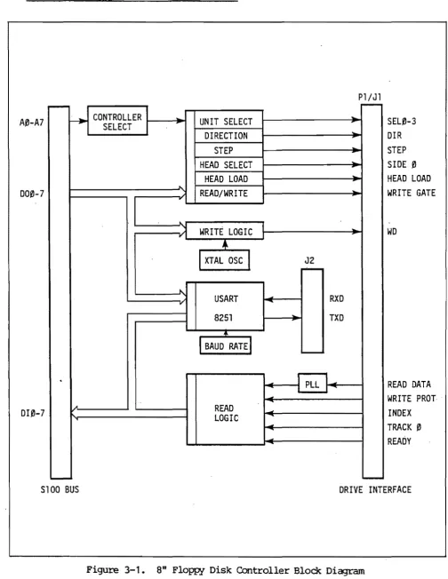
after a signal designation in the text means that signal is inverted (e.g.,"DDEN" is not inverted,"DDEN/" is inverted).As a suwlenent to the theory of operation see schematic drawing and the block diagrams shown in figures 3-1 and 3-2. A description of the various circuits on the Disk Controller board are discussed below.
3.1 Power Supply Section
'Ihe Disk Controller Board requires +5 Volts, +12 Volts, -5 Volts, and -12 Volts. These are provided by on-board voltage regulators driven from unregulated OC voltages of the 5-100 bus. 'Ihese voltages are filtered by a series of 4.7 uF capacitors.
A 7805 regulator provides the +5 Volts, a 7812 the +12 Volts, a 79L05 the -5 Volts, and a 7912 the -12 Volts.
3.2 Address Decoding
U32, U21, and IC U7 make up the Address Decode Circuit. Jumper area E selects 3 high order bits of the address so the board can be junpered for a base address of EOH. E6H - E7H select the 8251 USARI' and EOH - E3H select the 1793 Formatter/Controller.
3.3 BS-232C Drivers
Jumper areas C and D on the schematic can be used to select the board for either DTE (Data Terminal Equi:prent) or DCE (Data Ccmnunication Equipment)
via RS-232C handshaking lines. .
In order to control an RS-232C harrlshaking line fran the 8251, a signal must pass from an 8251 output pin to the input of one of the driver circuits in a 1488 quad-line driver, using the pads in junper area D. It must then pass fran the output of the 1488, where it is inverted, to the RS-232C line, using the pads in jumper area C.
To respond to an incoming RS-232C handshaking line, the signal must pass through the pads in jumper area C to the input of one of the receiver circuits in a 1489 quad-line receiver. It must then pass from the output of the 1489, where it is inverted, through the pads in junper area D, to one of the input pins of the 8251.
3.4
va>
and Data SeparatorThe VCO (Voltage Control Oscillator U27, U28) takes raw data from the disk arrl synchrooizes the Read Clock (Pin 26, 012 00 schematic) to data.
vector 8" Floppy Disk COntroller Manual
3.5 Clock Generator
.
The Clock Generator provides an 8 MHz clock to the Write Precompensation Circuit aOO a 2 MHz clock to the COntroller.
3.6 Write Precatp:nsation
The data written to the diskette is compensated during the write operation. This is called precornpensation. This means that certain data patterns will be shifted slightly reducing the margin for error in the read process. This shift is due to the magnetic recording process. The Shift Register U38 receives a 2 MHz pulse from the clock Generator which is clocked by the sane clock that operates U12. U39 is a multiplexer which selects the appropriate bit time in the shift register according to the output fran the clock generator. The output of U39 is sent to the disk drive where it is recorded on the diskette.
3.7 Drive Select Decoder
The Drive Select Decoder takes data bits from the 5-100 bus and decodes
two of them into the 4 drive select lines. Bits 0 aOO 1 are decoded as the
4 Drive Select lines, bit 2 selects the side of the disk, and bit 3 selects double density enable.
3.8 Progaaauable cammdcation Interface - 8251 Cllip
The 8251 is a Universal Synchronous/Asynchronus Receiver/Transmitter (USARl') chip. The USARl' accepts data characters from the CPU in parallel form and converts them into a continuous serial data stream for transmission. Simultaneously, it can receive serial data streams and convert them into parallel data characters for the CPU. The USARl' will signal the CPU whenever it can accept a
new
character for transmission or whenever it has received a character for the CPU. EIA RS-232C line driversand receivers interface the RxD and TxD output of the 8251 to the outside world. Discrete components are used to interface with 20 rnA teletype signals.
3.9 Disk Formatter and COntroller - 1793 Chip
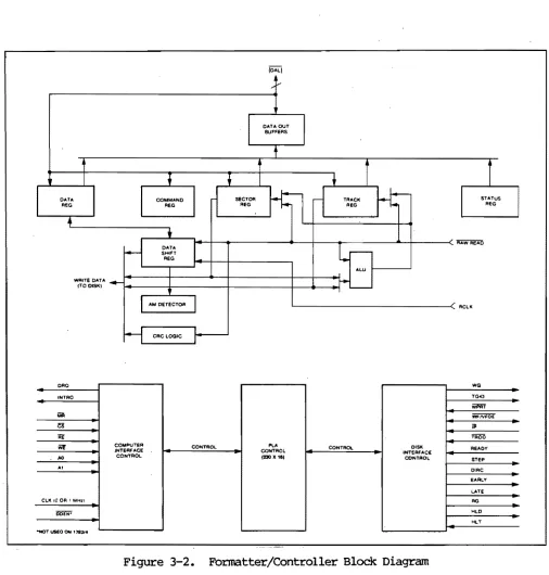
The heart of the Disk Controller Board is the 1793 Floppy Disk Formatter/Cootroller IC. A general description of this device can be found in Section I of this manual. A Block Diagram of the 1793 can be found in Figure 3-2.
RJl'E:
In the following discussion DAL refers to the 8 data access lines. See 3.9.1 for more details.
Data Shift Register
This 8-bit register assembles serial data from the Read Data input (RAW
vector
8" FlOW Disk Controller Manual.~
A0-A7
~CONTROLLER
SELECT
UNIT SELECT
DIRECTION
STEP
HEAD SELECT
HEAD LOAD
.1>.
000-7
rREAD/WRITE
~
/1
WRITE LOGIC
~
I
XTAL OSC
I
""
yUSART
8251..
I
BAUD RATE
I
.
DI0-7
.ALOGIC
READ
-J2
I""---
RXD
..
TXD
" "
-J
I
-
IPLL
I ......
~
"'
~
P1/J1
-""
..
-...
..
-SEL0-3
DIR
STEP
SIDE
0HEAD LOAD
WRITE GATE
WD
READ DATA
WRITE PROT
INDEX
TRACK 0
READY
S100 BUS
DRIVE INTERFACE
Figure 3-1. 8" Floppy Disk Controller Block Diagram
Vector 8- FloR'Y Disk Controller Manual
READ/) durirg read q>erations and transfers serial data to the Write Data output during write q>erations.
Data Register
This 8-bit register is used
as
a holding register during Disk Read and Write operations. In Disk Read operations the assembled data byte is transferred in parallel to the Data Register from the Data Shift Register. In Disk Write operations information is transferred in parallel from the Data Register to the Data Shift register.When executin::; the Seek canmaoo, the Data register holds the address of the desired track position. This register is loaded from the DAL and gated into the DAL under processor control.
Track Register
This 8-bit register holds the track number of the current Read/Wtite head position. It is incremented by one every time the head is stepped in (Towards tra.ck 76) and decremented by one when the head is stepped out (toward track 00) if the verify flag is on. The contents of the register are compared with the recorded track number in the 10 field durirg disk Read, Write, aoo Verify operations. The Track Register can be loaded fran or transferred to the DAL. This register should not be loaded when the device is busy.
sector Register (SR)
This 8-bit register holds the address of the desired sector position. The contents of the register are a:::rrpared with the recorded sector number in the ID field during disk Read or Write operations. The Sector Register contents can be loaded from
or
transferred to the DAL. This register shouldnot be loaded when the device is rosy.
Camrand Register (CR)
This 8-bit register holds the command presently being executed. This register should not be loaded when the device is busy unless the new canmaoo is a forced interrupt. The ccmmand register can be loaded from the DAIs, but the contents cannot be placed onto the DAL.
Status Register (STR)
This 8-bit register holds device status inforIlliation. The rreaning of the status bits is a function of the type of canmaoo previoosly executed. This register can be read onto the DAL but cannot be loaded from the DAL.
CRC Logic
This logic is used to dleck or to generate the 16-bit Cyclic Redundancy Check (CRC). The CRC includes all information starting with the address marl::
•
vector
8- Floppy Disk Controller
Manual
"r.-OATAOUT
I
SUFFERS
1
t
t
I
r
I
t
•
I
~I
DATAI
COMMANO SECTORKl~
TRACK~
STATuSR£G REG REG REG .£G
I
+
•
-1
OATAL-
RAW REAOSHiFT REG
I ALU
W{~~~~~A . . . . -
,
I1
-"JAM OEn.CT~ RelK
--1
CRC LOCiICORO WCi
tNTRO TO"3
iiil'i!T
MIl f'tfNFO£
~ iI'
R£ TAOO
;or COMPUTER INTERFAa. COfrllTAOl PI.A CONTROL DISK REAOY'
CONTROl. INTERFACE
/Ol CONTROL (ZIO.1I1 CONTAOI. STep
AI OlRe
EARLY
.... TE
eLK I~ Of!. I MH11 RG
0'ii'E'N- "LO
"LT
....or US£O ON 17'811"
Figure
3-2.Formatter/Controller Block
Diagramvector
8- FlOW' Disk Controller Manualaoo up to the CRC characters. The CRC register is preset to ones prior to data being shifted through the circuit.
Aritlnnetic/Iogic Unit (AW)
The ALU is a serial comparator, incrementer, and decrementer and is used for register rocdification and comparisms with the disk recorded
m
field.Tindng and Centrol
All computer and Floppy Disk Interface controls are generated through the logiq. The internal device timing is generated from an external crystal clock.
The 1793 has two different rro:'les of operation acoording to the state of DDEN/. When DDEN/
=
0, double density (MFM) is assumed. When DDEN/=
1, single density (FM) is assl..Ulled.AM Detector
The address mark detector detects ID, data and index marks during read
and write q;:>erations.
3.9. 1 Processor Interface
The interface to the processor is accomplished through the eight Data Access Lines (DAL/) aoo associated control signals. The DAL/ are used to transfer data, status, and control words out of,
or
into the 1793. The DAL/ are three state buffers that are enabled as output drivers when Chip Select (CS) and Read Enable (RE/) are active (low logic state) or act as input receivers when CS/ and Write Enable (WE/) are active.When transfer data with the Floppy Disk Controller is required by the host processor, the device address is decoded and Cs/ is made low. The
address bits A1 and AO oombined with signals RE/ during a read operation or WE/ during a write q;:>eration are interpreted as selecting the following registers:
A1-AO
a
0o
11 0
1 1
RFAD (REI)
Status Register Track Register Sector Register Data Register
WRITE (WE/)
Command Register Track Register Sector Register Data Register
During Direct Memory Access (DMA) types of data transfers between the Data Register of the 1793 and the processor, the Data Request (DRQ) output is used in Data transfer control. This signal also appears as status bit 1 during Read and Write operations.
On Disk Read operations the Data Request is activated (set high) when an assembled serial input byte is transferred in parallel to the Data register. This bit is cleared when the Data Register is read by the processor. If the
vector
8n Floppy Disk cattroller ManualData Register if;l read after ooe or nore characters are lost, by having new data transferred into the register prior to processor readout, the lost data bit is set in the Status Register. The Read operation continues until the end of the sector is readled.
On'Disk Write operations the data request is activated when the Data Register transfers its contents to the Data Shift register, and requires a
new data byte. It is reset when the Data Register is loaded with new data by the processor. If new data is not loaded at the time the next serial byte is required by the Floppy Disk, a byte of zeroes is written on the diskette and the lost data bit is set in the Status register.
At the oompletion of every CX>l'lIllaOO an INl'RQ is generated. INl',RJ is reset by either reading the Status register or by loading the Command register with a
new
CX>l'lIllaOO. In addition, INl',RJ is generated if a force interrupt o:mnand condition is met.3.9.2 Floppy Disk Interface
The 1793 has t;wc,) Irodes of operation according to the state of DDEN/ (Pin
37) • When DDEN/
=
1, single density is selected. In ei ther case, the CLK input (Pin 24) is at 2 MHz. However, when interfacing with the mini-floppy, the CLK input is set at 1 MHz for roth single density and double density. When the clock is at 2 MHz, the stepping rates of 3, 6, 10, and 15 IDS areobtainable. When CLK
=
1 MHz, these tiIres are doubled.Bead Positiarlng
Five commands cause positioning of the Read-Write head (see COmmand
Section). The period of each positioning step is specified by the r field in bits 1 and 0 of the command \«)rd. After the last directional step, an additional 15 IDS of head setting tiIre takes place if the verify flag is set
in Type I ccmnands. Note that this time doubles to 30 InS for a 1 MHz clock.
If TESl'/ = 0, there is 0 setting tiIre. There is also a 15 ms head setting time if the E flag is set in any Type II or III command.
The rates (shown in table 1) can be applied to a Step-Direction Motor through the device interface.
Step - A 2 us (MPM) or 4 us (FM) pulse is provided as an output to the drive. For every step pulse issued, the drive llOVes one track location in a direction determined by the direction output.
Direction (DllC) - The direction signal is active high when stepping in and low when stepping out. The direction signal is valid 12 us before the first stepping pulse is generated.
When a Seek, Step, or Restore command is executed, an optional verification of Read~ite head position can be performed by setting bit 2
(V = 1) in the camnand \«)rd to a logic 1. The verification operation begins at the end of the 15 millisecond setting time after the head is loaded against the media. The track number from the first encountered ID field is
vector 8- Plqpt Disk COOtroller Manual
crnpared against the oontents of the track register. I f the track numbers
compare and the ID field Cyclic Redundancy Check (CRC) is correct, the verify operation is conplete an] an ~ is generated with no errors. The
1793 must find an ID field with correct track number and correct CRC within 5 revolutions of the media; othe:t:Wise the seek error is set
am
an INTRQ is generated.elK 2 MHz 2 MHz 1 MHz 1 MHz 2 MHz 1 MHz
DDEN 0 0 x X
A1 RO TEST:1 TEST:l TEST"1 TEST=1 TEST"O TEST=O
STEPPING RATES 0 0 3 ms 3 ms 6 ms 6 ms 200 }loS 4001'8
0 1 8ms 6 ms 12 ms 12 ms 200 }loS 400 }loS
1 0 lOms 10 ms :<Oms 20 ms 2OO}IoS 4OO}IoS
1 1 15 ms 15 ms 30ms 30 ms 200 p.S 4OOp.s
The Head Load (HID) output oontrols the llOvement of the read/write head against the media. HLD is activated at the beginning of a Type I COIIIl1aIrl if the h flag is set (h == 1), at the end of a Type I ccmmand if the verify flag
(V == 1), or upcn the receipt of any Type II or III command. Once HLD is active, it remains active until either a Type I command is received with (h
== 0 and V
=
0li
or if the 1793 is in an idle state (nm-busy) and 1 5 index pulses have occured.Head Load Timing (HLT) is an input to the 1793 which is used for the head engage time. When HLT = 1, the 1793 assumes the head is completely engaged. The head engage time is typically used to fire a one shot. The output of the one shot is then used for HLT and supplied as an input to the 1793.
Hl.off-- _ ...
HEAD LOAD TIMING
I---SOTO l00mS--I
/---1
Ii.
-HI. T (FROM ONE SHOT)
When both HLD and HLT are true, the 1793 will then read from or write to the media. The "and" of HID and HLT appears as a status bit in Type I statU$.
In sumnary for the Type I COOItlaI¥ls: if h
=
0 and V == 0, HLD is reset. If h = 1 and V = 0, HID is set at the beginning of the ccmmand and HLT is not sanpled nor is there an internal 15 IllS delay. If h = 0 and V=
1, HID isset at the beginning of the ccmnand. Near the end of the corm:nand, after all the steps have been issued, an internal 15 IllS delay occurs
am
the 1793 then. waits for HLT to occur.
vector
8- FIOB?Y Disk Controller ManualFor Type II
am
III comnarrls with E flag off, HID is made active and HLT is sampled until true. With E flag on, HLD is made active, an internal 15InS delay occurs
am
then HLT is sampled until true.3.9.3 Disk Read Operations
Sector lengths of 128, 256, 512, or 1024 are obtainable in either FM or MFM formats. For FM, OOEN/ should be placed to logical "1." For MFM
formats, OOEN/ should be placed to a logical "0. It Sector lengths are determined at format time by a special byte in the "IO" field. If this sector length byte in the IO field is 0, then the sector length is 128 bytes. If 01, then 256 bytes. If 02, then 512 bytes. If 03, then 1024 bytes. The number of sectors per track as far as the 1793 is concerned can
be from 1 to 255 sectors. The number of tracks as far as the 1793 is concerned is from 0 to 255 tracks. For IBM 3740 compatibility, sector lengths are 128 bytes with 26 sectors per track. For System 34 compatibility (MFM), sector lengths are 256 bytes/sector with 26 sectors/track~ or lengths of .1024 bytes/sector with 8 sectors/track.
For read operations, the 1793 requires RAW READ/ Data (Pin 27) signal which is a 250 ns pllse per flux transition
am
a read clock (RCLK) signal to indicate flux transition spacings. The RCLK (Pin 26) signal is provided by sare drives but if not it may be derived externally by Phase lock loops, one shots, or counter techniques. In addition, a Read Gate Signal is prO\Tided as an output (Pin 25) which can be used to inform phase lock loops when to acquire synchronization. When reading from the m:!dia in FM,. RG is made true when 2 bytes of zeroes are detected. The 1793 must find an address mark within the next 10 bytes; otherwise RG is reset and the search for 2 bytes of zeroes begins allover again. If an address mark is found within 10 bytes, RG remains true as long as the 1793 is deriving any useful information fran the data stream. Similarly for MFM, RG is made active when four bytes of "00" or tiFF" are detected. The 1793 must find an address mark within the next 16 bytes, otherwise RG is resetam
search resumes.During read operations (w.;
=
0), the VFOE/ (Pin 33) is provided for phase lock loop synchrmization. VFOE/ will go active when:a) Both HLT and HLD
are
true.b) Settling ti.Ire, i f prCXJranured, has expired. c} The 1793 is inspecting data off the disk.
If WF/VFOE/ is not used, leave open or tie to a 10K resistor to +5. 3.9.4 Disk Write Operation
When writing is to take place on the diskette, the Write Gate (w.;) output is activated, allowing current to flow into the Read/Write head. As a precaution to erroneous writing, the first data byte must be loaded into the data l:egister in respcnse to a data request fran the 1793 before the Write Gate signal can be activated.
Writing is inhibited when the Write Protect/ input is a logic low, in which case any write command is immediately terminated, an interrupt is generated
am
the Write Protect status bit is set. The Write Fault input,vector
8- FlOB'X' Disk Controller Manualwhen activated, signifies a writing fault condition detected in disk drive electronics such as failure to detect write current flow when the write gate is activated. On detection of this fault, the 1793 terminates the current command and sets the Write Fault bit (bit 5) in the status word. The Write Fault/ input should be made inactive when the Write Gate output becomes inactive.
For write operations, the 1793 provides Write Gate (Pin 30) and Write Data (Pin 31) outputs. Write data consists of a series of 500 ns pulses in
rM (DDEN/
=
1)am
250 ns pulses in MFM (DDEN/=
0). Write Data provides the unique address marks in both formats.Also during write, two additional signals are provided for write precompensation. These are EARLY (Pin 17) and LATE (Pin 18). EARLY is active true when the WI) pulse appearing on (Pin 30) is to be written early.
LATE is active true when the WD pulse is to be written late. If both EARLY and LATE are low when the WI) pulse is pt:esent, the WI) pulse is to be written
at nominal. Since write precompensation values vary fran disk manufacturer to disk manufacturer, the actt.iaJ. value is determined by several one shots or delay lines which are located external to the 1793. The write p:recompensation signals EARLY and LATE are valid for the durat ion of WD in both PM and MFM formats.
Whenever a Read or write 00IIIt'Ia.J"d (Type II or III) is received, the 1793 samples the Ready input. If this input is logic low, the ccmmand is not executed and an interrupt is generated. All type I camnands are performed regardless of the state of the ready input. Also, whenever a Type II or III
conmand is received, the TG43 signal output is uplated. 3.9.5 Cauaand Description
The 1793 will accept eleven commands. Command words should only be loaded in the Corrmand Register when the Busy status bit (Status bit 0) is off. The one exception is the Force interrupt canmand. Whenever a CX')f['II'I1BIl is being executed, the Busy status bit is set. When a cc:::mna.rrl is conpleted, an interrupt is generated and there Busy status bit is reset. The Status Register indicates whether the completed conmand encountered an error or was faul t free. For ease of discussion, canmands are divided into four types. Corrmands and types are summarized below.
3.9.6 Type I CcIIInands
The Type I Commands include the Restore, Seek, Step, Step-in, and Step-out commands. Each of the Type I Commands contains a rate field
(rOr1), which determines the stepping lOOtor rate.
'lhe type I COftI1la.Irls contain a head load flag (h) which determines if the head is to be loaded at ~e beginning of the canmand. If h
=
1, the head is loaded at the beginning of the C'OIllItla.OO (HID output is made active). If h =0, HLD is deactivated. Once the head is loaded, the head will remain engaged until the 1793 receives a conmand that specifically disengages the head. If the 1793 is idle (busy
=
0) for 15 revolutions of the disk, thevector
8n Floppy Disk Controller Manualhead will be automatically disengaged (HID made inactive).
'lbe Type I Conmands also contain a verification (V) flag whidl determines if a verification q;>eration is to take place en the destination track. If V = 1, a verification is performed, if V = 0, no verification is performed.
During verification, the head is loaded and after an internal 15 rns delay, the HLT input is sampled. When HLT is active (logic true), the first encountered ID field is read off the disk. The track address of the ID field is then compared to the track register; if there is a matdl and a valid ID CRC, the verification is complete, an interrupt is generated and
the busy status bit is reset. If there is not a matdl but there is valid ID
CRC, an interrupt is generated, and Seek Error Status bit (status bit 4) is set and the busy status bit is reset. If there is a matdl but not a valid CRe, the eRe error status bit is set (Status bit 3), and the next encountered ID field is read from the disk for the verification operation. If an ID field with a valid CRC cannot be found after four revolutions of
~ disk, the 1793 terminates the operation_ and sends an interrupt (INTRQ).
The Step, Step-in, and Step-out commands contain an update flag (U). When U
=
1, the track register is updated by one for eadl step. When U=
0,the track register is not updated. " Restore (Seek Track 0)
Upon receipt of this ccmmand, the track 00 (TRX)/) input is sampled. If TRCO/ is active low, indicating the Read-Write head is p:>sitioned over track 0, the Track Register is loaded with zeroes and an interrupt is generated. If TROD/ is not active low, stepping pulses (Pins 15 and 16) at a rate specified by the r1rO field are issued until the
TRX)/
input is activated.At this tine the Track Register is loaded with zeroes and an interrupt is
generated." If the TROD input does not go active low after 255 stepping pulses, the 1793 "terminates operation, interrupts, and sets the Seek error status bit. A verification operation takes place if the V flag is set. The h bit allows the head to be loaded at the start of comnand. Note that the restore command is executed when MR/ goes from an active to an inactive state.
Seek
'lbis camnand assumes that the Track Register contains the track number of the current position of the Read-write head and the Data Register contains the desired track number. The 1793 will update the Track Register and issue stepping pulses in the appropriate direction until the contents of the Track Register are equal to the contents of the Data Register (the desired track location). A verification q;>eration takes place if the V flag is on. The h bit allows the head to be loaded at the start of thew camnand. An interrupt is generated at the cx:::ltl?letion of the corrmand.
Step
Upon receipt of this ccmmand, the 1793 issues one stepping pulse to the
vector
8" Floppy Disk COntroller Manualdisk drive. The stepping rotor direction is the same as in the previous step command. After a delay determined by the r1rO field, a verification takes place if the V flag is
on.
If the U flag is on, the track registeris
updated. The h bit allows the head to be loaded at the start of the
oomnand. An interrupt
is
generated at the oonpletion of the conrnarrl.Step-In
Upon receipt of this canmand, the 1793 issues one stepping pulse in the direction toward track 76. If the U flag is on, the track register is incremented by one. After a delay determined by the r1rO field, a verification takes place if the V flag is on. The h bit allOttls the head to be loaded at the start of the command. An interrupt is generated at the oonpletion of the COIIIIIaI'Xi.
Step-Out
Upon receipt of this canmand, the 1793 issues one stepping pulse in the direction towards track O. If the u flag is on, the Track Register is decremented by one. After a delay determined by the r1rO field, a verification takes place if the V flag is on. The h bit allOttls the head to be loaded at the start of the command. An interrupt is generated at the oonpletion of the cormnand.
3.9.1 Type II Ccmnands
The Type II commands are the Read Sector and write Sector commands.
Prior to loading the Type II COlYIllaI'X'i into the 0::mtla00 Register, the canputer must load the Sector Register with the desired sector number. Upon receipt of the Type II ccmnand, the busy status bit is set. If the E flag = 1 (this is the normal case), HLD is made active and HLT is sanpled after a 15 msec delay.· If the E flag is 0, the head is loaded and HLT sampled with no 15 msec delay.
When an to field is located on the disk, the 1793 compares the track number on the ID field with the Track Register. If there is not a match, the next encountered to field is read and a comparison is again made. If there was a match, the sector number of the ID field is canpared with the Sector Register. If there is not a Sector match, the next encountered ID field is read off the disk and comparisons again made. If the 10 field CRC is correct, the data field is then located and will be either written into or read from depending upon the command. The 1793 must find an ID field with a track number, sector number, side number, and CRC within four revolutions of the disk~ otherwise, the Record not found status bit is set (status bit 3) arrl the oommarrl is terminated with an interrupt.
Each of the Type II Commands contains an (m) flag which determines if multiple records (sectors) are to be read or written, depending on the
command. If m = 0, a single sector is read or written and an interrupt is generated at the ~letion of the corrmarrl. If m = 1, multiple records are read or written with the sector register internally updated so that an address verification can occur 00 the next record. The 1793 will continue
vector 8" Floppy Disk COntroller Manual
to read or write multiple records and update the sector register until the
sector register exceeds the number of sectors on the track or until the
Force Interrupt command is loaded into the command register, which
terminates the command and generates an interrupt.
If the Sector Register exceeds the number of sectors on the track, the
Record-Not-Found status bit will be set.
The Type II coomands also contain side select conpare flags. When C
=
0,no side canparison is made. When C = 1, the LSB of the side number is read
off the ID field of the disk and conpared with the contents of the (S) flag.
If the S flag compares with the side number recorded in the 10 field, the
1793 oontinues with the ID search. If a comparison is not made within 5
index pulses, the interrupt line is made active and the Record-Not-Found
status bit is set.
Read Sector
Upon receipt of the Read Sector command, the head is loaded, the Busy
·Status bit set, and when an 10 field is encountered that has the correct
track number, correct sector number, correct side number, and correct CRC,
the data field is presented to the cx:>mputer. The data Address Mark of the
data field must be found within 30 bytes in single density and 43 bytes in
double density of the last 10 field CRC byte, if not, the Record Not Found
status bit is set and the operation is terminated.
When the first character or byte of the data field has been shifted
through the OSR, it is transferred to the OR, and DR.2 is generated. When
the next byte is accumulated in the OSR, it is transferred to the OR and
another ORQ is generated. If the computer has not read the previous
contents of the OR before a new character is tranferred, that character is
lost and the Lost Data Status bit is set. This sequence continues until the
oonplete data field has been inputted to the computer. If there is a CRC
error at the end of the data field, the CRC error status bit is set and the
CX>llIllalld is terminated (even if it is a multiple record corrmand).
At the end of the Read operation, the type of oata Address Mark
encountered in the data field is recorded in the Status Register (bit 5) as
shown below.
srA'.lUS
BIT 5
1
o
Deleted Oata Mark Data MarkWrite Sector
Upon receipt of the write Sector ccmnand, the head is loaded (HLD active)
and the Busy status bit is set. When an 10 field is encountered that has
the correct track number, correct sector number, correct side number, and
Vector 8n
Floppy Disk Controller Manual
ccrrect CRC, a DR;;} is generated. The 1793 counts off 11 bytes in single density and 22 bytes in double density from the CRC field and the Write Gate
(W3) output is made active if the DRQ is serviced (i.e., the DR has been
loaded into the computer). If DRQ has not been serviced, the canmand is terminated and the Lost Data status bit is set. If the DRO has been serviced, the WG is made active and six bytes of zeroes in single density ani 12 bytes in double density are then written a l the disk. At this time
the Data Address Mark is then written on the disk as determined by the ao
field as shown below. ao
1
o
DATA ADDRESS MARK (Bit 0)
Deleted Data Mark data Mark
The 1793 then writes the data field ani generates DRQ's to the computer. If the DR;;} is not serviced in time for continuous writing, the Lost Data Status bit is set and a byte of zeroes is written on the disk. The canmand is not terminated. After the last data byte has been written on the disk, the two-byte CRC is COl'lplted internally and Written on the disk followed by me byte of logic mes in PM and MFM. The W3 output is then deactivated. 3.9.8 Type III Canoands
Read Mdress
Upon receipt of the Read Mdress camnand, the head is loaded and the Busy
Status bit is set. The next encountered ID field is then read in from the disk, and the six data bytes of the ID field are assembled and transferred to the DR, and a DR;;} is generated for each byte.
Although the CRe characters are transferred to the computer, the 1793 checks for validity
am
theCRe
error status bit is set if .there is a eRe error. The Track Address of the ID field is written into the sector register. At the em of the operation, an interrupt is generated and the Busy Status is reset. .Read Track
Upon rece ipt of the Read Track ccmnand, the head is loaded and the busy status bit is set. Reading starts with the leading edge of the first encountered index pulse and continues until the next index pulse. As each byte is assembled, it is tranferred to the Data Register and the Data Request is generated for each byte. No CRC checking is performed. Gaps are included in the input data stream. The accumulation of bytes is syncpronized to each Address Mark encountered. Upon completion of the
oomnand, the interrupt is activated. RG is not activated during the Read Track camnand.
Write Track
Upon receipt of the Write Track canmand, the head is loaded and the busy status bit is set. Writing starts with the leadlng edge of the first
vector 8" FlOI!'Y Disk Controller Manual
encountered index pllse and continues until the next index pulse, at which
time the interrupt is activated. The data request is activated imnediately
up:::n receiving the c:omma.rrl, but writing will not start until after the first
byte has been loaded into the Data register. If the DR has not been loaded by the time the index pulse is encountered, the operation is terminated making the device not busy, the Lost Data Status Bit is set, and the
interrupt is activated. If a byte is not present in the DR when needed, a
byte of zeroes is substituted. Mdress Marks and CRC dlaracters are written
on the disk by detecting certain data byte patterns in the outgoing data
stream. The CRC generator is initialized when any data byte from F8 to FE
is atout to be transferred fran the DR to the DSR in PM or by receipt of FS
in MFM.
3.9.9 ~ IV
c.armaoo
Force Interrupt
This command can be loaded into the camnand register at any time. If
there is a current command under execution (Busy Status Bit set), the
command will be terminated and an interrupt will be generated when the
oondition is specified in the 10 and 13 field is detected. The interrupt
conditions are shown below:
10 = Not Ready-To-Ready Transition
Ii = Ready-To-Not-Ready Transition
12 = Every Index Pulse
13 = Immediate Interrupt (requires reset, see note)
NOTE: If 10 - 13
=
0, there is no interrupt generated but the currentccmnand is terminated and busy is reset. '!his is the only camnand that will enable the immediate interrupt to clear on a subsequent Load Command
Register or
Read
Status Register.Status Description
Up:::n receipt of any ccmnand, except the force interrupt ccmnand, the Busy
Status bit is set and the rest of the status bits are updated or cleared for
the new cc:m:nand. If the Force Interrupt ccmnand is received when there is a
c..-urrent conmand under execution, the Busy status bit is reset, arrl the rest
of the Status bits are unchanged. If the Force interrupt command is
received when there is not a current command under execution, the Busy Status bit is reset and the rest of the status bits are updated or cleared.
In this case, status reflects the Type I cooma.rrls.
Rev. 1-A 1/23/81
WRITE
J
GATE~
TWOr-
TBC---jiWPl-WRITE DATA
EARLY
OR
LATE
IF ON
WRITE DATA TIMING
.... __ - - - -~ .6" OR 32"
US---""I1
VOH
ORQ
INf~O
--I
VOLVil
~ VIH
115ACT
'---+---1~~~..t---AAWA60 RCLK DISKETTE 8" 8" 5" 5"
NOTE 1 a 1iM1 IE PERMANINfL't TIED LOW I' OE$IAID
"nMf, OOU8US WHEN CLOCK' UM·il
t SERvICE (WOAST CASEl
"FM 21S uS "MfM ~ 13.5 uS
READ ENABLE TIMING
I
I tbe
rpw
---1
I--1
TXI
I==T.,-I
-I
I
,
~T'
. I ·
r.- i
I To I
NOMINAL
MODE DDEN eLK T. T~ T,
MFM 0 2 MHz 1 ",s 1 ",s 2 ",s
FM 1 2 MHz 2 ",s 2",s 4",s
MFM 0 1 MHz 2",s 2",s 4J.iS
FM 1 1 MHz 4 ",s 4 "'s 8 "'s
INPUT DATA TIMING
3-16
vector 8· Floppy Disk Controller Manual
ORQ
lNTAO
We
OiL
t." OR 32" uS.---~-i
1---1 'seRVICE VOl
JI
TSlfVOl
VI"
Non 1 CS MA't 8E PeRMANENTLY TIEO lOW IF DESIRED
2 WHEN wAITING DATA INTO SECTOR, TRACK OR OAT A REGISTER USEA CANNOT A£AO THIS FlEGiSTER UNTIl AT LEAST" ~EC tNM'M,vTERTHfiFUSINGEOGEOFWE
t SEAVICE {WORST CASE} WHEfrrt WfUTINQ iNTO "tHE: COtMrr.tAHO REGISTER STATUS ·FM '" 235 uS IS NOT VALID UNTIL SOME It ~EC tN N 6 ~c IN MFM
~MFM ;\ J t 51,t$ LATEA Tt1£SE TIMES ARE DOUBLED WHEN Clk • 1 MHI
'TIME': OOu8LES WHEN CLOCK ;\ 'MHz
WRITE ENABLE TIMING
iP j
J
I/Ijotr--
TIP--1Wi j
I
I
; VItt!--TWF
--1
MAI
I
~ Vijolf-
T " A - l !-TCYC-!ClK
LrL
--1:t
!-_TCO'alAe vOI+
.-J
STEP'"
J~
VOL
1-
TOIA~TST'I----1TSTP
f--
t--
TOIA --jrSTPf--STEP
~~
.Ol
MISCELLANEOUS TIMING
vector
8" Floppy Disk COntroller ManualIV. Tests and Mjustments
4.1 Controller Mjust:D.l':mts
Controller adjustments consist of: a. Center frequency adjust.
b. 1 us single-shot adjust. c. 0.5 us single-shot adjust. 4.1.1 Test COnfiguratial
a. Insert the controller in an 5-100 bus 8080/Z80 based computer using an exterrler card.
b. Connect controller to any Data·-Trak 8 storage IOOdule.
4.1.2 Center Fr~<.y Mjust Test Procedure a. Ensure that the drive is not on.
b. Connect oscilloscope to oscillator at Al5-7. Set oscilloscope time base to 200 ns/cm.
c. Measure frequency of oscillator. 4.1.3 1 us S!!tsle-Shot Mjust Test Procedure
a. Insert a diskette in drive.
b. Position the head to track 0
am
write a full track of I ones I data (16 sectors).c. Perform a continuoos read operation 00 track zero.
d. Alternately select program X14 to achieve steps b and c.
e. Connect oscilloscope to A14-S. Set time base of oscilloscope to 200
ns/cm and observe one-shot output.
4.1.4 0.5 us Single-Shot Mjust Test Procedure
a. Proceed with steps a thru d, paragraph 2.1.3.
b. Connect oscilloscope to A14-3. Set time base of oscilloscope tp 200
ns/cm and observe one-shot output.
vector 8" Floppy Disk Controller Manual
4.1.5 l\cceptable Limits
a. Center Frequency: 970 KHz minimum - 1033 KHz maximum.
b. 1 us single-soot: 1.94 us minimum - 2.06 us maximum. c. 0 .5 us single-shot: 0.97 us minimum - 1.03 us maximum.
4. 1 .6 Mjust:nent Procedure
a. Center frequency: Adjust R40 until output frequency is 0.5 MHz. b. 1 us single-smt: Adj ust R27 for a period of 1 us.
c. 0.5 us single-shot: Adjust R46 for a period of 0.5 us.
: ~ t : :J(~ ~11 "j (" ~ ~ ~~ 1(:
:1=
~
~ ~..
~~ ..
•
.
.
-
=.
~.
.
= z ~5
.
z ; "~l'
"
; •-
: : : ;;-.
\.; ~
. .
.
;;.
.
uf"
" e
.
-
" ;!--
!--~'7
.
"lV•
I !I 5;;: ~=. i :pd
.
.
:
i..
..
.
: e :. .
II i =+
.
;<
:: ftl
a
I .M
5) d
i
II- =;:-
:
.
t~
i