Optical Wavelet Signals Processing and Multiplexing
Gabriella Cincotti
Department of Applied Electronics, University Rome Tre, Via della Vasca Navale 84, 00146 Roma, Italy Email:[email protected]
Michela Svaluto Moreolo
Department of Applied Electronics, University Rome Tre, Via della Vasca Navale 84, 00146 Roma, Italy Email:[email protected]
Alessandro Neri
Department of Applied Electronics, University Rome Tre, Via della Vasca Navale 84, 00146 Roma, Italy Email:[email protected]
Received 31 March 2004; Revised 1 February 2005
We present compact integrable architectures to perform the discrete wavelet transform (DWT) and the wavelet packet (WP) de-composition of an optical digital signal, and we show that the combined use of planar lightwave circuits (PLC) technology and multiresolution analysis (MRA) can add flexibility to current multiple access optical networks. We furnish the design guidelines to synthesize wavelet filters as two-port lattice-form planar devices, and we give some examples of optical signal denoising and compression/decompression techniques in the wavelet domain. Finally, we present a fully optical wavelet packet division multi-plexing (WPDM) scheme where data signals are waveform-coded onto wavelet atom functions for transmission, and numerically evaluate its performances.
Keywords and phrases:optical communication system, wavelet transforms, wavelet packet division multiplexing, planar lightwave circuits, optical signal processing.
1. INTRODUCTION
Global communication networks infrastructure has been ex-panded thanks to recent advances in optical technology, such as transparent photonic switches and ultra-long-haul trans-mission systems, and the increase of multimedia data traf-fic is strengthening the demand for ultra-high-capacity pho-tonic networks. The key feature of ultrafast optical networks is that the electrical conversion is avoided until data signals reach the most external edge node. Optical signal processing is not only faster than the electrical one, but it can also sup-port a larger throughput, and current optical networks are evolving toward solutions where photonic routers are replac-ing electronic routers in the intermediate nodes [1].
In the present paper, we show that the use of wavelet functions in optical communications can provide an overall capacity improvement thanks to the two-dimensional pro-cessing capability of multiresolution analysis (MRA), and we present different architectures in standard planar lightwave circuits (PLC) technology that perform the wavelet analysis and multiplexing of data signals directly in the optical do-main.
The wavelet transform involves joint time-frequency rep-resentation of nonstationary signals using compactly sup-ported basis functions, and MRA has been extensively used to solve a large variety of problems in different research ar-eas. The enormous flexibility in the choice of the wavelet al-lows the use of optimal wavelets for specifical applications, such as image compression, signal denoising, human vision, radar, earthquake prediction, and computer vision problems, such as range detection or motion estimation [2,3,4]. In optics communications, wavelets have been used for time-frequency multiplexing [5,6] and ultrafast image transmis-sion [7]. In general, wavelet signal analysis is associated with an effective computational algorithm, even faster and simpler than the fast Fourier transform (FFT) algorithm [8].
describe some optical implementations for the DWT and WP decomposition. Some numerical examples for optical signal denoising and compression are given inSection 4; in partic-ular, we show that the SNR of an optical signal can be en-hanced by performing the DWT of the optical signal and thresholding the detail coefficients. In addition, we evidence the correspondence of the wavelet analysis and the optical packets compression/decompression method using delay line lattice structures [9]. Finally, inSection 5we present an in-novative full optical wavelet packets division multiplexing (WPDM) scheme and numerically test its performance.
The huge bandwidth provided by optical fibers and the capability of signal processing directly in the optical layer make an attractive combination for future multiple access networks. The feasibility of optical code division multiple ac-cess (O-CDMA) systems has been demonstrated where the spectral [10] or the temporal [11] encoding results in spread-ing the optical pulse in the frequency or the time domain. However, a more efficient use of the time-frequency plane has the potential of proving flexible access to a larger num-ber of multiple end users. WPDM is an emerging technique, used in wireless communications, that transmits message sig-nals overlapped in time and frequency domains, and recovers them with very low multiple access interference (MAI) noise, thanks to the orthogonal properties of the wavelet packet functions [12,13,14,15]. Data signals from different users are waveform-coded onto wavelet atom functions and trans-mitted in a multiple access network. Wavelet atom functions are self-orthogonal against integer translations and mutual-orthogonal due to different subbands occupancy; these prop-erties ensure a better use of time-frequency plane, with re-spect to standard time division multiplexing (TDM), wave-length division multiplexing (WDM), and CDMA systems [12]. In its standard form, WPDM requires N waveform shapers to code each user bit sequence with a different wave-form, and its optical implementation is impracticable [5]. We present a compact, full optical WPDM scheme, where the transmitter is a single encoder that multipliesNoptical data signals fromN simultaneous users. The encoder gives the equivalent sequence at the root of the WP decomposi-tion tree, and it is followed by a single modulator that com-pletes the waveform coding, shaping the optical pulses of the composite signal with the scaling function profile. The re-ceiver is a reversal version of the transmitter, and the same optical devices are used for both encoding and decoding the binary sequences. In addition, we show that both the WP encoder/decoder and the waveform modulator can be fabri-cated using PLC technology and integrated on a single de-vice: the WP encoder/decoder can be realized as a tree of lattice-form optical delay line filters [16], whereas the modu-lator as a weight/phase-programmable tapped delay line filter [17].
2. MULTIRESOLUTION ANALYSIS
The analysis of nonstationary signals involves a compromise between how well transitions or discontinuities are located,
and how finely long-term behavior can be identified. For in-stance, standard Fourier transform decomposes a continu-ous time-signals(t) into individual frequency components, using complex sinusoidal basis functions exp(iωt), that are infinite in extent. As these basis functions are periodic, any short duration signal spreads over the whole basis. In con-trast, the MRA decomposes a signal at different scales or res-olutions, using a basis whose elements are localized in both time and frequency domains, and the representation of short duration and nonstationary signals focuses on a few compo-nents, that immediately enlighten the predominant frequen-cies and the time occurrence of abrupt changes.
Specifically, the continuous wavelet transform (CWT) performs correlations between the signals(t) and scaled ver-sions of themother waveletψ(t):
CWTs(a,τ)= 1
|a|
s(t)ψ∗
t−τ a
dt, (1)
whereais a real nonzero scale parameter, andτthe transla-tion factor. Ifψ(t) satisfies theadmissibility condition
cψ= ψ(f)
2
|f| df <∞, (2)
whereψ(f) is the Fourier transform of the mother wavelet
ψ(t), the signals(t) can be reconstructed by means of the in-verse wavelet transform
s(t)= 1
cψ
CWTs(a,τ)1
|a|ψ
t−τ a
da dτ a2 . (3)
Usuallyψ(t) is localized both in time and frequency domains, and the CWT displays the time evolution of the frequency components of a signal. In fact, by applying the Fourier Par-seval formula [18], (1) can be rewritten as
CWTs(a,τ)=
|a|
˜
s(f)ψ∗(−a f)e−j2π f τdf, (4)
where ˜s(f) is the Fourier transform of the signal. There-fore, the CWT can be seen as the output from a bank of fil-ters which are constructed by dilatations/compressions of the mother wavelet. Filters obtained by dilatations ofψ(t) pro-cess the low-frequency information of the signals(t), whereas the filters related to the compressed version ofψ(t) analyze the high-frequency content.
More useful in digital signal processing and multiplex-ing are the orthogonal wavelet series expansions, derived from the CWT when scale and translation factors are con-strained to discrete values. Let φ(t) be a (smooth) scaling function such that the discrete set of functions{2−/2φ(2−t− k∆τ) (,k∈Z)}forms an orthonormal basis for a subspace
V ∈ L2(R); here∆τ is a time interval that will coincide
of functions{2−/2ψ(2−t−k∆τ) (,k ∈ Z)}forms an
or-thonormal basis for a subspace W ∈ L2(R); (b) the
sub-spacesV andWare mutually orthogonal, that is,W⊥V;
(c) the subspaceV−1can be expressed as direct sum ofV
andW, namely
V−1=V⊕W. (5)
Then, a signals(t) ∈ V0 is represented by a smoothed
ap-proximation at resolution 2M, obtained by combining
trans-lated versions of the basic scaling functionφ(t), andMdetails at the dyadic scalesa=2(=1, 2,. . .,M−1) obtained by
combining shifted and dilated versions of the mother wavelet
ψ(t):
s(t)=
k
2−M/2cM[k]φ 2−Mt−k∆τ
+
M
=1
k
2−/2d[k]ψ 2−t−k∆τ.
(6)
The wavelet and the scaling function satisfy thedilation equa-tions
φ(t)=√2
k
h[k]φ(2t−k∆τ),
ψ(t)=√2
k
g[k]φ(2t−k∆τ),
(7)
whereg[k] andh[k] are the coefficients of two quadrature mirror filters (QMFs)
H(ω)=√1 2
k
h[k]e−jωk∆τ,
G(ω)=√1 2
k
g[k]e−jωk∆τ,
(8)
and∆τis the inverse of their FSR [19,20].
The DWT is computed by using Mallat’s pyramidal algo-rithm [8]. Letc0[n] be the expansion coefficients of the signal
s(t)∈V0, with respect to the orthonormal basisφ(t−∆nτ):
c0[n]=
s(t),φ(t−n∆τ)=
s(t)φ∗(t−n∆τ)dt, (9)
where angular brackets indicate inner product. Then the co-efficientsc0[n] can be decomposed into the scaling coeffi
-cientsc1[n] and detail coefficientsd1[n], via recursive
dis-crete convolutions with the lowpassh[n] and highpassg[n] filters, respectively, followed by subsampling of factor 2:
c1[n]=
k
c0[k]h[2n−k],
d1[n]=
k
c0[k]g[2n−k].
(10)
c0[n]
h[n] c1[n] h[n]
c2[n] h[n] g[n]
23 23 c3[n] d3[n]
g[n] 22 d2[n]
g[n] 2 d1[n]
Figure1: Pyramidal decomposition scheme for the DWT: an opti-cal signal is driven into the device input and the optiopti-cal wavelet de-tail and scaling coefficients are obtained at the device outputs. The output signals have to be subsampled according to their decompo-sition level.
The DWT decomposition halves the time resolution and doubles the frequency resolution, because the frequency band of the output signals spans only half of the frequency band of the original signal; therefore, half of the samples can be discarded by subsampling, without any information loss. On the other hand, the reconstruction process yields the in-put sequence by the inverse filtering and upsampling:
c0[n]=
k
c1[k]h[2k−n] +d1[k]g[2k−n]. (11)
The decomposition procedure can be further repeated, and, at each decomposition level, the filtering and subsampling halves both the number of the samples and the frequency band:
c[n]=
k
c−1[k]h[2n−k],
d[n]=
k
c−1[k]g[2n−k].
(12)
Here,c[k] andd[k] are the scaling and the details coeffi -cients, respectively, at resolution 2. This approach reduces
w0,0[n]
h[n] w1,0[n] h[n] w2,0[n]
h[n] g[n] 23
w3,0[n]
23 w3,1[n]
g[n] w2,1[n]
h[n] g[n] 23
w3,2[n]
23 w3,3[n]
g[n] w1,1[n] h[n] w2,2[n]
h[n] g[n] 23
w3,4[n]
23 w3,5[n]
g[n] w2,3[n]
h[n] g[n] 23
w3,6[n]
23 w3,7[n]
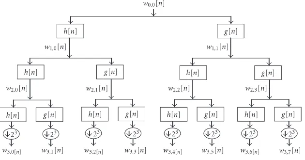
Figure2: Pyramidal scheme for the WP decomposition: an optical signal is driven into the device input and the optical wavelet packet coefficients are obtained at the device input. The decomposition level is=3, and all the output signals have to be subsampled at 2=8.
The WP decomposition offers a richer signal analysis, with respect to DWT, as both the scalingc[n] and the detail coefficientsd[n] are recursively decomposed, following the same filtering and subsampling scheme [3]. The decomposi-tion tree corresponding to a full WP analysis is illustrated in
Figure 2: in this case, all the outputs have the same number of samples and span over the same frequency bandwidth, be-cause they correspond to the same decomposition level. The WP decomposition is performed by computing the convolu-tion of the input signalc0[n] with the wavelet atom functions
that are a set of functions defined in the following recursive manner:
w+1,2m(t)=
k
h[k]w,m t−2k∆τ
,
w+1,2m+1(t)=
k
g[k]w,m t−2k∆τ
.
(13)
Hereis the decomposition level,m(0≤m≤2−1) the
wavelet atom position in the tree [4]; in addition, the func-tionw0,0(t) coincides with the scaling functionφ(t). By
ex-ploiting the recursive structure of (13), a wavelet atom func-tion can be expressed as
w,m(t)=
k
f,m[k]φ(t−k∆τ), (14)
with f,m[n] being the equivalent filter from the root to
the (,m)th terminal, that can be recursively evaluated us-ing (13). The WP atoms are self- and mutual-orthogonal functions at integer multiples of dyadic intervals [21]:
w,m t−2nτ
wλ,µ t−2λkτ
=δ[−λ]δ[m−µ]δ[n−k],
,λ∈Z, 0≤m≤2−1, 0≤µ≤2λ−1, n,k∈Z.
(15)
This property, that is, the waveform orthogonality is used in the WPDM to transmit multiple message signals over-lapped in time and frequency domains.
3. SYNTHESIS OF OPTICAL WAVELET FILTERS
To implement the DWT or the WP decomposition of an op-tical signal, we consider the tree structures of Figures1and2, where each pairH(ω) andG(ω) of QMFs is synthesized as a two-port lattice-form planar filter. If an optical digital signal, with bit rateBis driven into the device input, at the device outputs we obtain the DWT or the WP decomposition, up to theth level. In the standard MRA, the outputs have to be subsampled at a factor 2, so that the total number of the bits
in the input signal coincides with the total number of bits in all the wavelet coefficient signals.
In [22], we presented the design guidelines to synthesize optical wavelet filters, following the algorithm proposed by Jinguji and Oguma [23] and using the powerhalf-band(HB) property of wavelet filters:
H(ω)2
+G(ω)2=1,
G(ω)=e−jω∆τH∗
ω+ π
∆τ
.
(16)
Jinguji and Oguma showed that an optical HB filter of length
M can be fabricated using a Mach-Zehnder interferometer (MZI) with a path delay difference ∆τ, andM/2−1 MZIs with a path delay difference of 2∆τ [23]. The first MZI has an input 3 dB coupler and no phase shifter inserted in its arms; the remaining circuit parameters can be calculated by applying a recursive algorithm. The synthesis procedure of QMFs is quite immediate, as the circuit parameters are di-rectly related to the filter coefficients [22]. For instance, the Daubechies wavelet filters of lengthM=2, also known as the Haar wavelet, are
HdB1
GdB1
=√1
2
1 1 1 −1
. (17)
d1[n]
∆τ
π/4 π/4 c1[n]
d2[n]
2∆τ π/4 π/4
c2[n]
d3[n]
4∆τ π/4 π/4c
3[n]
Figure 3: Optical architecture for the DWT with Daubechies wavelet of lengthM=2. Each optical wavelet filter is an MZI with input/output 3 dB couplers, and FSR that decreases from the root to the leaves in a logarithmic way.
with input/output 3 dB couplers; furthermore, the FSRs in the decomposition tree decrease from the root to the leaves in a logarithmic way, since at each decomposition level, the subsampling halves the signal frequency band.
The QMFs of Daubechies wavelet of lengthM=4 are
HdB2
GdB2
= 1
4√2
1−√3 3−√3 3 +√3 1 +√3 1+√3 − 3+√3 3−√3 − 1−√3
,
(18)
and the WP decomposition corresponds to the circuital scheme ofFigure 4.
4. OPTICAL WAVELET SIGNAL PROCESSING
Wavelets are a powerful tool to denoise signal corrupted by white Gaussian noise [24,25,26]. The denoising scheme is based on the principle of selective wavelet reconstruction: in fact an inhomogeneous signal compacts into just a few wavelet coefficients, whereas white noise is distributed over a large number of coefficients, and, therefore, it can be reduced by thresholding the detail wavelet coefficients. The denoised signal is then obtained by inverse wavelet transforming the thresholded coefficients.
The time and frequency localization properties of the wavelet transform can also take the chromatic dispersion into account, since dispersion affects only the detail coefficients that represent highpass-filtered versions of the original sig-nal. In this case it is necessary to perform a selective recon-struction of the wavelet coefficients that will be the subject of a next paper.
To give a numerical example of the proposed denois-ing method, we consider a 128-bit-long pseudorandom bit sequence (PSRS) atB =10 Gbps modulated by an external Mach-Zehnder modulator with 30 dB extinction ratio; the signal SNR ratio is 24 dB. The device of Figure 3performs the DWT of the optical signal atλ=1550 nm, composed of Gaussian pulses ofδt=20 ps width; the FSR is chosen equal to 16/δt. At the device outputs we obtain the scaling coeffi -cientsc3[n] at the third level of decomposition (=3), and
all the detail coefficientsd[n]( = 1, 2, 3), that are plotted inFigure 5. It is evident that all the detail coefficients are the highpass-filtered version of the signal, and they can be sup-pressed to eliminate the noise; therefore, the denoised signal is reconstructed using only the scaling coefficientsc3[n]. The
eye diagram of the original and the denoised signals are re-ported in Figure 6and we observe a significative
improve-ment in the eye opening. We also remark that the efficiency of the denoising method depends on the wavelet choice, and the threshold selection rules. In the previous example, we consider a very simple case, where all the detail coefficients have been completely eliminated, but better performances can be achieved with optimal thresholding methods.
To quantify the SNR improvement, inFigure 7we plot both the SNR and the BER of the denoised signal, as func-tions of the SNR of the input signal, and we observe that the SNR is increased by more than 10 dB.
The device of Figure 3 can be also used to com-press/decompress optical data in ultrafast packet-switched networks. In fact the delay lattice scheme proposed by To-liver et al. in [9] is an incomplete DWT scheme that evalu-ates only the scaling coefficientsc[n]. In this case, the unit delay∆τequates the difference between the pulse periods in the uncompressed and compressed signals. It is evident that a standard DWT or a full WP decomposition allows a larger variety of compression/decompression methods.
5. OPTICAL WAVELET PACKET DIVISION MULTIPLEXING
The success and widespread use of code division multiple access (CDMA) in the wireless domain has renewed inter-est in exploring its use in the optical domain, which, how-ever, presents a different set of challenges [27]. In an optical CDMA (O-CDMA) network, the information sequences are codified in time, using temporal codes, or in frequency do-main with standard diffraction-based spread-spectrum tech-niques. Recently, hybrid techniques have been proposed to manage burst changes of data traffic or increasing requests of new data services [28]. O-CDMA can support high-capacity services, broadband signals processing, and multiplexing of a large number of users; in addition, many approaches have been proposed to avoid the optical-electrical-optical con-version, that severely limits the transmission system perfor-mances.
We present an all-optical WPDM system that makes a very efficient use of time-frequency plane. The digital se-quences from each user are encoded by a set of orthogo-nal waveforms [12]: the orthogonal properties of the wavelet atoms and their overlapping nature in time and frequency yield an overall system capacity improvement [5].
The TDM sequenceσ,m[n] from themth user at bit rate B = 1/T is waveform-coded by the wavelet atom function
w,m(t):
s,m(t)=
n
σ,m[n]w,m t−2n∆τ
, (19)
and summed together with the waveform-coded signals from the other 2−1 users:
sc(t)=
2−1
m=0
n
σ,m[n]w,m t−2n∆τ
∆τ 2∆τ π/4 5π/3 π/12
w1,1[n]
2∆τ 4∆τ π/4 5π/3 π/12
w1,0[n]
2∆τ 4∆τ π/4 5π/3 π/12
w2,3[n] 4∆ τ 8∆τ π/4 5π/3 π/12
w2,2[n] 4∆τ 8∆τ π/4 5π/3 π/12
w2,1[n] 4∆τ 8∆τ π/4 5π/3 π/12
w2,0[n] 4∆τ 8∆τ π/4 5π/3 π/12
w3,7[n] w3,6[n] w3,5[n] w3,4[n]
w3,3[n] w3,2[n] w3,1[n] w3,0[n]
Figure4: Optical architecture for the WP decomposition with Daubechies wavelet filter of lengthM=4. Each optical wavelet filter is a chain of two MZIs, with FSR that decreases from the root to the leaves in a logarithmic way.
Theprocessing gainof the WPDM system is equivalent to the O-CDMA parameter and is expressed as the ratio of the time duration of the waveform and the input signal widthδt
[29]:
F=2∆τ
δt . (21)
For a correct waveform shaping, it is necessary that the input bit durationδtequates the inverse of the FSR, that is,
δt =∆τ: in this way, each optical pulse is transformed into the corresponding wavelet atom function at the device out-put. Therefore, the processing gainF=2equates the
num-ber of simultaneous users.
A standard WPDM transmission system consists of a bank of waveform modulators, one for each user, and its op-tical implementation is really complex [5]. A more compact WPDM architecture, with a single WP encoder and only one waveform modulator, can be designed by “reversing” the ex-pression of (20) for the composite signalsc(t). In fact, if we substitute (14) into (20), we obtain
sc(t)=
2−1
m=0
n σ,m[n]
k
f,m[k]φ
t− 2n+k∆τ
=
i
σ[i]φ(t−i∆τ),
(22)
where
σ[i]=
2−1
m=0
n f,m
i−2nσ
,m[n] (23)
is the equivalent sequence from all the users obtained at the root of the WP tree [12]. From an inspection of this equation,
it is evident that the composite signal sc(t) can be gener-ated by first encoding all the input sequence σ,m[n] from
each user with a WP encoder, thus obtainingσ[i], and then waveform shaping all the composite bits by the scaling func-tion φ(t) [6]. This WPDM architecture is schematically il-lustrated inFigure 8: the WPDM transmission system is im-plemented by the WP encoder of Figure 2, followed by a single modulator that shapes the multiplexed optical pulses
σ[i] with the scaling function profile φ(t). The receiver is a time reversal version of the transmitter, and the WP de-coder follows the pulse shaper; therefore, the same device can be used for both encoding and decoding the binary se-quences.
The time gating opens a time window to extract the au-tocorrelation peak and it is somewhat equivalent to narrow-bandpass filtering in the wireless CDMA. The use of a time gating before detection significantly relaxes the requirements for the detector bandwidth to the bit rate of 2∆t. The
syn-chronization from the time gating can be derived from the recovered clock.
The optical architecture for a WP encoder/decoder is identical to an optical WP decomposition scheme, so that the scheme ofFigure 4can be thought of as optical E/D for the Daubechies wavelets of lengthM=4.
In a WPDM system, each bit from each user is waveform-coded by wavelet atom functions, and all the data streams from the users are transmitted simultaneously. On the other hand, in a code-based O-CDMA system, a different code is assigned to each user; therefore, if we remove the pulse shapers in the transmission scheme of Figure 8, we obtain a standard O-CDMA system, where the input data signals are coded by optical orthogonal codes (OOCs) sequences [30]. In fact, the device of Figure 4 is a full optical E/D that codes/decodes binary sequences from 2 users
simul-taneously [31,32]; of course, for an O-CDMA system, it is
1 0.5 0
Si
gn
al
0 0.2 0.4 0.6 0.8 1 1.2 1.4 1.6 t(ns)
1 0.5 0
c3
0 0.2 0.4 0.6 0.8 1 1.2 1.4 1.6 t(ns)
0.1 0.05 0
d3
0 0.2 0.4 0.6 0.8 1 1.2 1.4 1.6 t(ns)
0.1 0.05 0
d2
0 0.2 0.4 0.6 0.8 1 1.2 1.4 1.6 t(ns)
0.1 0.05 0
d1
0 0.2 0.4 0.6 0.8 1 1.2 1.4 1.6 t(ns)
Figure5: Input optical signal atB=10 Gbps,λ=1550 nm, and SNR=24 dB; the Gaussian optical pulses have 20 ps width. Scaling coefficientsc3 that coincide with the denoised signal and
thresh-olded detail coefficients at levels 1, 2, 3 are obtained. The DWT is performed with the device ofFigure 3, with no subsampling.
To complete the waveform coding in a WPDM system, an optical pulse shaper is necessary. We consider two different devices; the first one is a diffractive pulse shaper, identical to an O-CDMA spread-spectrum encoder, composed of two diffraction gratings and an amplitude/phase filter [33]. The incoming pulses are spatially decomposed in their spectral components by the first grating, and an amplitude/phase mask gives the scaling function spectral profile to the radi-ation; the second grating reassembles the waveform-coded pulses. Otherwise, an optical pulse shaper can be fabri-cated as a weight/phase-programmable optical-tapped de-lay line filter [17]. In this case, both the WP E/D and the waveform shaper can be integrated on a single silica sub-strate.
To evaluate the detection capabilities of a full optical WPDM system, we generateN independent data signals at
B=10 Gbps modulated by 27−1 word length PRBSs, using
1 0.9 0.8 0.7 0.6 0.5 0.4 0.3 0.2 0.1
Le
ve
l
1 2 3 4 5 6 7 8 9 10
Normalized symbol number (a)
1 0.9 0.8 0.7 0.6 0.5 0.4 0.3 0.2 0.1
Le
ve
l
1 2 3 4 5 6 7 8 9 10
Normalized symbol number (b)
Figure6: Eye pattern diagrams of the input signal and the denoised signal ofFigure 5.
external Mach-Zehnder modulators with 30 dB extinction ratio. Each user bit sequence is forwarded to theNinputs of the encoder ofFigure 4and the encoder output is waveform-modulated by the pulse shaper corresponding to the scal-ing wavelet of the Daubechies filters of length M = 4, as illustrated inFigure 8.Figure 9shows the signal-to-MAI ra-tio as a funcra-tion of the number of the simultaneous users
N, that is evaluated as the ratio between the signal cor-responding to a “1” from the ith user and the signal de-tected at the same output when the ith user is transmit-ting a “0” and all the other N −1 users are transmitting a “1.”
40 35 30 25 20 15 10
SNR
out
10 12 14 16 18 20 22 24
SNRin
(a)
10 10−2 10−4 10−6 10−8 10−10 10−12
BER
8 10 12 14 16 18 20 22 24
SNRin
BERout
BERin
(b)
Figure7: (a) SNR of the denoised signal (that coincides with the scaling coefficientsc3from the device ofFigure 3) versus the SNR of the
input optical signal. (b) Bit error rate of the input signal (solid line) and the denoised signal (dotted line) versus the SNR of the input signal.
WP E/D
Waveform modulator
Waveform modulator
WP E/D
Time gating
σIm[n] σ[i] sc(t)
δt 1/B Input bit
∆t
WP-coded
2∆t 1/B WP waveform-modulated
Matched
Unmatched
1/B 1/B
1/B 1/B
Figure 8: Schematic of an optical WPDM system: the data se-quences fromN users are WP-encoded by a single optical device; the composite signal is then waveform-modulated by a pulse shaper. The receiver is a reverse version of the transmitter.
6. CONCLUSION
We present a complete overview of the wavelet signal pro-cessing and multiplexing in the optical domain, using passive PLC devices.
We describe the PLC architectures to perform the DWT and the WP decomposition of an optical digital signal, and furnish the design guidelines to synthesize a wavelet filter as a two-port lattice-form planar device. We demonstrate that within the MRA it is possible to both denoise and
29.2 29.1 29 28.9 28.8 28.7 28.6 28.5 28.4 28.3
Si
gn
al-t
o-MAI
ratio
(dB)
0 20 40 60 80 100 120 140 160 180 200 N
Figure9: Signal-to-multiple-access-interference ratio (dB) versus the numberNof simultaneous users.
compress/decompress data streams directly in the optical do-main; in addition we evidence the large flexibility of the pro-posed approaches, thanks to the possibility to choose the op-timal wavelet.
The WP encoder/decoder and the pulse shaper are low-loss compact devices that can be fabricated using standard PLC technology and integrated together on a single common mechanically rigid substrate, avoiding undesirable variations of optical path lengths over time, temperature, and exposure to mechanical vibrations. The possibility of growing or prun-ing the wavelet decomposition tree allows to adapt the multi-ple access system to different traffic requirements, adding or dropping data streams.
The optical signal processing fully exploits the fibre band-width, and it is suitable for broadband multiple access net-works. The proposed devices can be employed in ultrafast and highly-robust multiple access networks and their low cost, compactness, and fabrication simplicity, make them at-tractive for an ever-increasing number of different applica-tions.
REFERENCES
[1] K.-I. Kitayama and N. Wada, “Photonic IP routing,” IEEE Photon. Technol. Lett., vol. 11, no. 12, pp. 1689–1691, 1999.
[2] E. A. Rosenfeld,Multiresolution Techniques in Computer Vi-sion, Springer-Verlag, New York, NY, USA, 1984.
[3] J. J. Benedetto and M. W. Frazier,Wavelets: Mathematics and Applications, CRC Press, Boca Raton, Fla, USA, 1994. [4] A. K. Louis and P. Maaß,Wavelets: Theory and Applications,
John Wiley & Sons, New York, NY, USA, 1997.
[5] T. Olson, D. Healy, and U. ¨Osterberg, “Wavelets in optical communications,”IEEE Computing in Science & Engineering, vol. 1, no. 1, pp. 51–57, 1999.
[6] G. Cincotti, M. S. Moreolo, and A. Neri, “All optical multi-plexing scheme for multiple access networks based on wavelet packets filter banks,” inProc. SPIE International Symposium Integrated Photonics Europe, Strasbourg, France, 2004. [7] T. Konishi and Y. Ichioka, “Ultrafast image transmission
by optical time-to-two-dimensional-space-to-time-to-two-dimensional-space conversion,”Journal of the Optical Society of America{A}, vol. 16, no. 5, pp. 1076–1088, 1999.
[8] S. G. Mallat, “A theory for multiresolution signal decompo-sition: the wavelet representation,”IEEE Trans. Pattern Anal. Machine Intell., vol. 11, no. 7, pp. 674–693, 1989.
[9] P. Toliver, K.-L. Deng, I. Glesk, and P. R. Prucnal, “Simulta-neous optical compression and decompression of 100-Gb/s OTDM packets using a single bidirectional optical delay line lattice,”IEEE Photon. Technol. Lett., vol. 11, no. 9, pp. 1183– 1185, 1999.
[10] R. P. Scott, et al., “Demonstration of an error-free 4 X 10-Gb/s multi-user SPEC O-CDMA network test bed,”IEEE Photon. Technol. Lett., vol. 16, pp. 2186–2188, 2004.
[11] K.-I. Kitayama, “Code division multiplexing lightwave net-works based upon optical code conversion,”IEEE J. Select. Ar-eas Commun., vol. 16, no. 7, pp. 1309–1319, 1998.
[12] K. M. Wong, J. Wu, T. N. Davidson, and Q. Jin, “Wavelet packet division multiplexing and wavelet packet design un-der timing error effects,”IEEE Trans. Signal Processing, vol. 45, no. 12, pp. 2877–2890, 1997.
[13] A. R. Lindsey, “Wavelet packet modulation for orthogonally multiplexed communication,”IEEE Trans. Signal Processing, vol. 45, no. 5, pp. 1336–1339, 1997.
[14] K. M. Wong, J. Wu, T. N. Davidson, Q. Jin, and P.-C. Ching, “Performance of wavelet packet-division multiplexing in im-pulsive and Gaussian noise,”IEEE Trans. Commun., vol. 48, no. 7, pp. 1083–1086, 2000.
[15] R. E. Learned, H. Krim, B. Claus, A. S. Willsky, and W. C. Karl, “Wavelet-packet-based multiple access communica-tion,” inWavelet Applications in Signal and Image Processing II, vol. 2303 ofProceedings of SPIE, pp. 246–259, San Diego, Calif, USA, October 1994.
[16] G. Cincotti, “Fiber wavelet filters,”IEEE J. Quantum Electron., vol. 38, no. 10, pp. 1420–1427, 2002.
[17] K.-I. Kitayama, S. Osawa, N. Wada, and W. Chujo, “Op-tical pulse train synthesis of arbitrary waveform using weight/phase-programmable 32-tapped delay line waveguide filter,” inOptical Fiber Communication Conference and Exhibit (OFC ’01), vol. 3, pp. WY3/1–WY3/3, Anaheim, Calif, USA, March 2001.
[18] R. N. Bracewell,The Fourier Transform and Its Applications, McGraw-Hill, New York, NY, USA, 1986.
[19] M. Vetterli and C. Herley, “Wavelets and filter banks: the-ory and design,”IEEE Trans. Signal Processing, vol. 40, no. 9, pp. 2207–2232, 1992.
[20] C. Herley and M. Vetterli, “Orthogonal time-varying filter banks and wavelet packets,” IEEE Trans. Signal Processing, vol. 42, no. 10, pp. 2650–2663, 1994.
[21] B. S. Krongold, K. Ramchandran, and D. L. Jones, “Frequency-shift-invariant orthonormal wavelet packet rep-resentations,”IEEE Trans. Signal Processing, vol. 47, no. 9, pp. 2579–2582, 1999.
[22] G. Cincotti, M. S. Moreolo, and A. Neri, “Synthesis of opti-cal wavelet filters,”IEEE Photon. Technol. Lett., vol. 16, no. 7, pp. 1679–1681, 2004.
[23] K. Jinguji and M. Oguma, “Optical half-band filters,”J. Light-wave Technol., vol. 18, no. 2, pp. 252–259, 2000.
[24] D. L. Donoho and I. M. Johnstone, “Ideal spatial adaptation by wavelet shrinkage,”Biometrika, vol. 81, no. 3, pp. 425–455, 1994.
[25] L. M. Johnstone and B. W. Silverman, “Wavelet threshold es-timators for data with correlated noise,”Journal of the Royal Statistical Society: Series B, vol. 59, pp. 319–351, 1997. [26] M. Lang, H. Guo, J. E. Odegard, C. S. Burrus, and R. O. Wells
Jr., “Noise reduction using undecimated discrete wavelet transform,”IEEE Signal Processing Lett., vol. 3, no. 1, pp. 10– 12, 1996.
[27] J. A. Salehi, “Code division multiple-access techniques in op-tical fiber networks. I. Fundamental principles,”IEEE Trans. Commun., vol. 37, no. 8, pp. 824–833, 1989.
[28] T. Pfeiffer, J. Kissing, J.-P. Elbers, et al., “Coarse WDM/CDM/TDM concept for optical packet transmis-sion in metropolitan and access networks supporting 400 channels at 2.5 Gb/s peak rate,”J. Lightwave Technol., vol. 18, no. 12, pp. 1928–1938, 2000.
[29] K.-I. Kitayama, N. Wada, and H. Sotobayashi, “Architectural considerations for photonic IP router based upon optical code correlation,”J. Lightwave Technol., vol. 18, no. 12, pp. 1834– 1844, 2000.
[30] T. Dennis and J. F. Young, “Optical implementation of bipolar codes,”IEEE J. Quantum Electron., vol. 35, no. 3, pp. 287–291, 1999.
[31] G. Cincotti, “Full optical encoders/decoders for photonic IP routers,”J. Lightwave Technol., vol. 22, no. 2, pp. 337–342, 2004.
[32] PCT patent Application No. PCT/IT03/000879 filed on December 30th 2003 by University Roma TRE, inventor Gabriella Cincotti.
Gabriella Cincottiwas born in Naples, Italy, in 1966. She received the Laurea (M.S.) degree (cum laude) in electronic engineering from University of Rome “La Sapienza” in April 1992. She was a project engineer at the Microwave Laboratory, Alenia, Aeritalia & Selenia S.p.A., Rome, from 1992 to 1994, and joined the Depart-ment of Applied Electronics, University Rome Tre, as an Assistant Professor, in October 1994. Her ongoing research areas include passive optical devices, as optical filters, wavelength demultiplex-ing, encoders/decoders, and polarizing devices. Her research results have been recorded in over 50 refereed papers and summarized in nearly 20 conference and symposium presentations. She is a Member of the IEEE Lasers and Electro-Optics Society (LEOS), the Consorzio Nazionale Interuniversitario per le Telecomunicazioni (CNIT), and the National Institute for the Physics of the Matter (INFM), University Rome Tre, Rome, Italy.
Michela Svaluto Moreolowas born in Rome, Italy, in 1977. She re-ceived the Laurea (M.S.) degree (cum laude) in electronic engineer-ing from University Rome Tre in May 2003. She is currently a Ph.D. student in telecommunication engineering at the University Rome Tre, Rome, Italy, since November 2003. Her research interests are in the field of passive optical devices, such as planar lightwave circuits and photonic bandgap structures. Her studies are directed towards all-optical signal processing in WDM systems and all-optical beam-forming in radio-over-fiber systems. Her research in nanophoton-ics involves also quantum dot lasers/LEDs. She is a Student Member of the IEEE Lasers and Electro-Optics Society (LEOS).