High Resolution Wide Dynamic Range for
Programmable Delay Generator for
Applications in Timing Spectroscopy
Shivali Dube1, Kanchan Chavan2, Dr.P.P.Vaidya3
PG Student [VESIT], Dept. of Instrumentation Engineering, VESIT, Chembur, Mumbai, India1 Assistant Professor, Dept. of Instrumentation Engineering, VESIT, Chembur, Mumbai, India2
HOD, Dept. of Instrumentation Engineering, VESIT, Chembur, Mumbai, India3
ABSTRACT: Timing spectroscopy requires the measurement of the time interval between two physical events. Timing spectroscopy used in various applications in the field of nuclear instrumentation, time correlated single photon counting, time of flight, positron annihilation spectroscopy, coincidence detection and discrimination of neutron gamma discrimination. Such timing spectroscopy systems require calibration units for their testing. These calibration units can measure the timing error existing in the timing spectroscopy system.High Resolution Wide Dynamic Range Programmable Delay Generator of 1ns to 1us with resolution 1ns is used to calibrate timing spectroscopy systems. This paper introduces study, Design and implementation of High Resolution Wide Dynamic Range system which gives variable delay logic pulse to calibrate timing spectroscopy systems. Aim is to develop system which produced variable delay logic pulse from 1nanosecond to 1microsecond with 1 nanosecond resolution & 1 nanosecond accuracy.
KEYWORDS:Timing Spectroscopy, Programmable delay generator, time-to-amplitude converter
I .INTRODUCTION
Timing spectroscopy involves the measurement of the time relationship between two events. a time-pickoff circuit is employed to produce a logic output pulse that is consistently related in time to the beginning of each input signal. Ideally the time of occurrence of the logic pulse from the time-pickoff element is insensitive to the shape and amplitude of the input signals.a time-to-amplitude converter (TAC) can be used to measure the time relationship between correlated or coincident events seen by two different detectors that are irradiated by the same source. Figure.1is a simplified block diagram of a typical time spectrometer used for making this type of timing measurement.
Fig.1 Block diagram of timing spectroscopy
I
nternational
J
ournal of
A
dvanced
R
esearch in
E
lectrical,
E
lectronics and
I
nstrumentation
E
ngineering
(An ISO 3297: 2007 Certified Organization) Website: www.ijareeie.com Vol. 6, Issue 1, January 2017
the time difference between the two signals. .Most important characteristic of TAC is its linearity over entire the conversion ranges. Walk, jitter this types of error introduced non-linearity in the measurement. The amplitude information from the TAC is often applied to an MCA for accumulation of the data and display of the probability density of start-to-stop time intervals, commonly called a timing spectrum. Timing spectroscopy systems accuracy needs to be measured and hence calibration units are required.
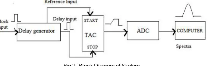
Fig 2. Block Diagram of System
Fig .2 shows design of calibration system of timing spectroscopy Systems.
In this Paper Introduced Programmable delay generator which produced variable delay logic pulse. The precise delay pulse applied to TAC.TAC was used to measure the delay time. The TAC was started by the Reference delay pulse signal of delay generator IC and stopped by its delayed pulse signal, the TAC result was digitized by an analog-to-digital (ADC) and after then a spectrum was created in a computer. Programmable delay generator system is used to calibrate timing spectroscopy system.
II. LITEARTURE SURVEY
A digitally-programmable method for linearly controlling signal delay over a wide frequency and delay range has been developed.Emitter degeneration or pre- or post-distortion techniques usually are needed to linearizethe relationship between voltage and delay. [1]
High Speed Multiple Pre-set Counter & Pulsed Crystal Oscillator Which Synchronized in constant phase with respect to random time Reference pulse, comprised a new precision Delay Generator.[7]
It described the system's composition in hardware and software view.This system is composed ofProgrammable gate arrays deserializer MAX3885, high-speed clock generator AD9517-1, DDR2 SDRAM, serializer and USB2.0 Controller.[9]
High timing-fidelity delay circuit because of engineering requirement and practical necessity. This high resolution delay circuit can also be used in other coincidence electronics designs that use the “timing-AND-logic” concept employed by some commercial PET systems because such systems also require a long delay to synchronize the timing trigger and the energy/position signals.[10]
The developed system is required to generate high-side (HS) and low-side (LS) signal in frequency range from 1 MHz to 15 MHz and duty cycle values from 5% to 50%. The most notable characteristic of the developed generator is the ability to adjust dead-times between the generated signals as precise as possible in order to use the signal generator for testing the semiconductor devices for synchronous DC-DC converter applications.[11]
II. PROGRAMMABLE DELAY GENERATOR STRUCTURE & DESIGN
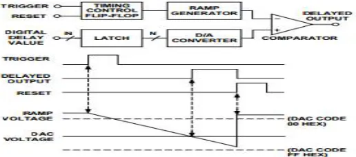
The operating principle of Programmable delay generator is as follows: A programmable delay generator delays pulse by a programmed amount of time. The delay through the device is controlled by an n-bit digital word. This is the programmed delay. Programmable delay generator internally makes use of ramp/comparator/DAC architecture as shown in figure 3. One input of a high-speed comparator is driven by a digital to-analog converter (DAC). The DAC is used to set a reference voltage at this comparator input. The other input is connected to a ramp generator. The ramp generator is started by applying a pulse to the trigger input of the delay generator. When the ramp voltage crosses the comparator, threshold set by the DAC, the output of the comparator switches. This output is delayed from the trigger pulse by an amount of time that is proportional to the DAC digital input code and the slope of the ramp. Altering the digital delay value changes the DAC output voltage, which alters the delay through the circuit.
Fig 3. Working principle of programmable delay generator IC
a) Block Diagram
Fig 4 show programmable delay generator system. Design included two delay generator ICs & DIP Switches. Programmable delay generator generates delay logic pulse which varies from nanosecond to microsecond with 1ns step size. The entire range is not covered by using a single programmable delay generator IC. Thereby, two programmable delay generator ICs are used to generate variable delay from nanosecond to microsecond. DS1023-100 which delay pulse from 16ns to 255ns with 1ns step size and DS1023-500 which delay pulse from 16ns to 1275microsecond with 5ns step size. Input signal is TTL pulse. Output pulse is delayed by an amount of time that is proportional to the digital input code, Digital inputs are produced by DIP switch’s, pulse then delay up to nanosecond to microsecond. To get 1 nanosecond resolution and 1 nanosecond accuracy cascade both the IC.as shown in figure 4.
Fig 4. Structure of programmable delay generator system
b) Operating Principle
I
nternational
J
ournal of
A
dvanced
R
esearch in
E
lectrical,
E
lectronics and
I
nstrumentation
E
ngineering
(An ISO 3297: 2007 Certified Organization) Website: www.ijareeie.com Vol. 6, Issue 1, January 2017
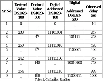
00000000 Addressed. because of DS1023-100 having limited delay range input TTL pulse delay by 250 ns with DS1023-500 at that time DS1023 -100 is With 00000000 Addressed. Now the output pulse is delay by 250 ns, after this step required delay is 251ns to 499ns that is done with DS1023-100, DS1023-500 is with 00000000 Addressed. When it reaches to 499ns the DS1023-500 is set to 500 ns. Again repeat the procedure increase delay with 1ns step size up to 749 ns with the DS1023-100. 750ns set with DS1023-500.This procedure is followed tocover the range up to 1000ns with 1ns accuracy and 1ns resolution. Fig.5.Describe the Operation Of Programmable Delay Generator System.
Fig.5.Operation of Programmable Delay Generator System
Table 1. Illustrate the processing of calibrate DS1023-500 IC with DS1023-100. Output of Programmable delay Generator system is 32ns for 00000000 Addressed.Reading was taken with respect to Reference Delay of DS1023-100.
Sr.No
Decimal
Value
DS1023-100
Decimal
Value
DS1023-500
Digital
Addressed
DS1023-100
Digital
Addressed
DS1023-500
Observed
delay
(ns)
1
0
_
0
_
16
_
_
_
_
_
_
2
233
_
11101001
_
247
3
_
47
_
101111
248
_
_
_
_
_
_
4
250
_
11111010
495
5
_
97
_
1100001
496
_
_
_
_
_
_
6
242
_
11111100
_
747
7
_
148
_
10010100
748
_
_
_
_
_
_
8
254
_
11111110
_
999
9
_
199
_
11000111
1000
Table.1. Calibration Reading
c) Reference Delay
a reference delay has been included on chip which may be used to compensate for the step zero delay. In practice this means that if the device is supplied with a clock, for example, the minimum programmed output delay is effectively zero with respect to the reference delay.
d) Timing Diagram of the System
The timing diagram of overall system is shown in Fig 6
OUT is a copy of the input waveform that is delayed by an amount set by the programmed values. A programmed value of zero will still result in a non-zero delay. The signal on OUT is the same polarity as the input. REF is a fixed reference delay. It also is a copy of the input waveform but the delay interval is fixed to a value approximately equal to the Step Zero Value of the device.
III. RESULT AND DISCUSSION
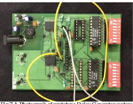
We have designed and implemented a high resolution programmable delay generator. Programmable Delay Generator System Generate Variable Delay From 1ns to 1us with 1ns Accuracy & 1ns Resolution. All the performance tests have been done on an independent prototype circuit see figure 7.Two Programmable Delay Generator ICs are Used. Both ICs Have its Limited Range. To Cover Entire Range Cascade Both ICs. An Input to Programmable Delay Generator System is TTL pulse Which Delay by the Output of System with 32 ns with input Addressed Code is oooooooo.To Get Minimum Delay Output Is Taken with Respect to Ds1023-100 Reference Delay.
Fig.7.A Photograph of prototype Delay Generator system
I
nternational
J
ournal of
A
dvanced
R
esearch in
E
lectrical,
E
lectronics and
I
nstrumentation
E
ngineering
(An ISO 3297: 2007 Certified Organization) Website: www.ijareeie.com Vol. 6, Issue 1, January 2017
jitter (resolution) of the rising-edge was measured. Programmable delay generator systems output from 16ns to 1000ns with 1ns step size & 1ns Resolution.
Fig.8.Input Pulse Delay by 16ns
In the Figure 8 Input Pulse Delay by 16ns When Input Digital Code is 00000000.This is Minimum Delay Taken With
respect To DS1023-100 Reference Delay.
Fig.9Input Pulse Delay by 1000ns
In the Figure 9Input Pulse Delay by 1000ns When Input Digital Code is Maximum. This is Maximum Delay Taken
With respect To DS1023-100 Reference Delay.
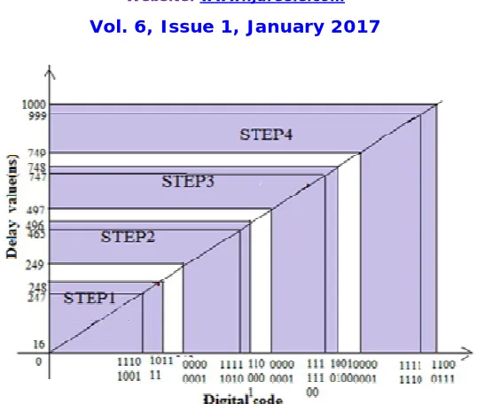
Fig.10 Observed Reading
Table 2shows the Observed Reading of Programmable Delay Generator System. The Entire Range Is Cover with Distributed Steps Which is The Combination of Both Delay Generator ICs.Programmable Delay Generator System Generate Delay from 16ns to 1us with 1ns Resolution & 1ns Accuracy.
STEP1
STEP2
STEP3
STEP4
DS1023-100
Generate
Delay
Value(ns)
DS1023-500
Generate
Delay
Value(ns)
DS1023-100
Generate
Delay
Value(ns)
DS1023-500
Generate
Delay
Value(ns)
DS1023-100
Generate
Delay
Value(ns)
DS1023-500
Generate
Delay
Value(ns)
DS1023-100
Generate
Delay
Value(ns)
DS1023-500
Generate
Delay
Value(ns)
16-247
248
249-495
496
497-747
748
749-999
1000
Table 2.the Observed Reading of Programmable Delay Generator System.
IV.CONCLUSION
A programmable high-resolution delay generator has been designed and constructed. Our test results showed: (1) the delay generator had a less than ±290ps timing jitter that was essential for timing and coincidence measurement (2) the total delay range of the delay generator could be 16 ns to 1us with no performance degraded; (3) the delay time can be programmed at a coarse step of 16.7ns and a fine step of 1ns. This high-resolution delay generator is use in calibration of timing spectroscopy. This delay generator can also be used as a general device in other applications such as automatic test equipment and communications.
REFERENCES
[1] S. L. Morton, K. Elliott and M. Rodwell, "High resolution 20 GHz wideband delay generator," in Electronics Letters, vol. 40, no. 20, pp. 1248-1249,30Sept.2004.doi: 10.1049/el:20046038
[2] Ray Marston, “Analog Delay Line”, Radio Electronics, October 1986
[3] G. F Knoll, Radiation Detection and Measurement, John Wiley and Sons, New York,NY (1979). [4] Allen Hill, IE “Digitally Programmable Delay Generators”, Analog devices.
I
nternational
J
ournal of
A
dvanced
R
esearch in
E
lectrical,
E
lectronics and
I
nstrumentation
E
ngineering
(An ISO 3297: 2007 Certified Organization) Website: www.ijareeie.com Vol. 6, Issue 1, January 2017
[6] S. Saha, F. Lesage and M. Sawan,“High-voltage pulse generator with variable delay forultrafast gating of single photon detector,” 2016 IEEE 7th Latin American Symposium
on Circuits Systems (LASCAS), Florianopolis, 2016, pp. 131-134.
[7] D. Hartke, M. Willrodt and D. Broderick, “A Precision Delayed Pulse Generator asa Variable Time Interval Standard,”12th Annual Symposium on Frequency Control,Asbury Park, NJ, USA, 1958, pp. 406-419
[8]Yaqiang Liu et al., "A programmable high-resolution ultra-fast delay generator," in IEEE Transactions on Nuclear Science, vol. 50, no. 5, pp. 1487-1490, Oct. 2003. doi: 10.1109/TNS.2003.817412
[9]S. Zhaolinet al., "High Resolution Programmable Digital Delay Generator Design and Realization," 2010 International Conference on Intelligent System Design and Engineering Application, Changsha, 2010, pp. 813-816.doi: 10.1109/ISDEA.2010.137
[10]Yaqiang Liu et al., "A programmable high-resolution ultra fast delay generator," 2002 IEEE Nuclear Science Symposium Conference Record, 2002, pp. 1153-1157 vol.2.doi: 10.1109/NSSMIC.2002.1239526
[11]F. Hormot, J. Bačmaga and A. Barić, "Dual-channel programmable precise time-delay pulse signal generator for synchronous DC-DC converter applications," 2015 38th International Convention on Information and Communication Technology, Electronics and Microelectronics (MIPRO), Opatija,2015,pp.98-102.doi: 10.1109/MIPRO.2015.7160246