High Field Electrical Conduction and
Breakdown in Solid Dielectrics
R.S.Pote1, V.N.Gohokar2, D.G.Wakde3, R.S.Kankale4
Associate Professor, Department of Electrical Engineering, SSGMCOE, Shegaon, India1,
Professor, Department of Electrical Engineering, All India Shri Shivaji Memorial College of Engineering, Pune, India2, Director, P.R.Pote Patil College of Engineering, Amravati, India3
Assistant Professor, Department of Electrical Engineering, SSGMCOE, Shegaon, India4
ABSTRACT: Insulator is an important part of the high voltage equipments. Various types of insulating materials are
used in high voltage electrical power system to protect all power system equipments. For the safety, reliability and efficiency, the insulating materials must be in a healthy condition during its operation. Most of the insulating materials are in impure form due to presence of air bubbles (cavity) or other impurities present inside the solid insulating materials. The local electrical breakdown occurring in solid dielectric is called as partial discharge (PD) which takes place due to the high voltage field stress. Due to the occurrence of PD the dielectric property of insulating materials deteriorates. Because of this reason detection of PD becomes one of the important tasks for high voltage engineers in order to keep the high voltage equipment in healthy condition. In this experimental model is used to study partial discharge and breakdown phenomena. For experimentation purpose sample of Acrylic material with cylindrical cavity is taken as a solid insulating material for creating partial discharge inside the solid dielectric by applying high voltage. In this study, partial discharge signal is captured with experimental setup at different high voltages which are further used for study and PD analysis.
KEYWORDS: Insulators, Partial Discharge, High Voltage, Cavity.
I. INTRODUCTION
II. PARTIAL DISCHARGE MECHANISM
As per IEC Standard 60270, Partial discharge is defined as a localized electrical discharge that partially bridges the insulation gap between the two conductors and which may or may not occur adjacent to a conductor. Concentration of local electrical stress in an insulation system or on the surface of insulation system results in occurrence of partial discharge. Such electrical discharges appear in the form of sharp impulses of various forms of voltage magnitude and current magnitude having short duration less than a sec. Generally PD occurs in high voltage equipments like transformer, insulators, cable etc. PD mainly occurs within cavities or voids inside a solid dielectric. It also occurs at interface between solid and liquid dielectric mediums, or in bubbles or air pockets inside liquid dielectrics. This discharge is limited to only over a portion of the insulation; the discharge partially bridges the gap between the two electrodes. PD can also take place along the insulation boundary between two insulating materials.
A. CLASSIFICATION OF PARTIAL DISCHARGE
Partial discharge phenomenon is divided into following two categories: (a) External partial discharge
The partial discharge which takes place outside the high voltage equipment is called as external partial discharge. Such type of discharge generally occurs in overhead transmission lines or on armature of machines.
(b) Internal partial discharge
The partial discharge which mainly occurs inside a system is called as internal partial discharge. The discharge occurring inside cavity is belonging to such type of partial discharge. Partial discharge includes several types of discharges like corona discharge, surface discharge, cavity discharge, Treeing and tracing phenomenon.
(i) Surface discharge: It takes place on interfaces of two different dielectric materials such as gas and solid interface due to high electric stressed in gas than solid material. This type of discharge may takes place in high voltage bushing, high voltage cable end, on insulator surface between electrodes.
(ii) Cavity discharge: Generally cavities are formed in solid or bubbles in liquid insulating materials. The cavity is filled with gas or air medium. Such discharge takes place when the gas within the cavity gets over stressed.
(iii) Corona discharge: It takes place due to non-uniform electric field distribution on the edges of conductor supplied with high voltage. Gas or air or liquid insulation is supplied for such type of discharge.
(iv) Treeing and tracing: High intensity electric fields are produced in an insulating material at its surfaces or edges which deteriorates the insulating material. This is responsible for the production of continuous discharge called as Treeing and tracking phenomenon.
B. EFFECT OF A PARTIAL DISCHARGE IN INSULATING SYSTEM
Occurrence of PD is the main cause for degradation of insulating material and responsible for electrical breakdown. Repetition of partial discharge phenomenon is the main reason for mechanical and chemical degradation or deterioration of the insulating material. The effect of this discharge is severe on insulation of high voltage power equipment. Insulation damage occurs due to formation of partial discharge. The conductivity of the insulating material is zero under normal operating condition but it rises due to chemical changes in the dielectric.
Dielectrics are classified into two types:
Inorganic dielectric and
Organic dielectric.
Generally immunity of organic dielectrics is less. Porcelain, glass, mica are belonging to inorganic type of dielectric. Polymer dielectrics are belonging to organic dielectrics category.
C. PD MEASURING CIRCUITS ACCORDING TO IEC 60270
Fig.1 shows the equivalent circuit diagram for the measurement of PD(partial discharge) as per IEC 60270. This setup consists of high voltage source, test object as per a-b-c model and measuring instrument.
Fig: 1: Equivalent circuit diagram used for PD measurement
There are various methods used for the measurement of partial discharge based on both electrical and non-electrical phenomena. Methods which have been popularly used for the measurement of partial discharges are:
• Optical method of detection • Acoustic method of detection • Chemical method of detection • Electrical method of detection
D. FACTORS AFFECTING THE DIELECTRIC STRENGTH OF INSULATING MATERIAL
Several studies are carried out to check whether the dielectric strength of insulating material is affected by some factors or conditions. The dielectric strength of any insulating material depends upon the temperature, impurity; spacing between two electrodes etc. and some other factors which are also responsible for it. In high voltage equipments the strength of liquid dielectric decreases to 70 % because of the presence of impurity content like suspended particles. Impurity includes solid particles of carbon, wax, and fiber. Presence of impurity contents creates imperfections in the insulation system.
III. NECESSITY OF DETECTION OF PARTIAL DISCHARGE
Most of the dielectric materials are in impure form from the origin. Due to the presence of impurity air bubbles are created within the insulating material. It minimizes the insulation property and responsible for the occurrence of partial discharge. The reason behind the formation of PD is the dielectric constant of the gas inside the cavity is less than that of surrounding medium. This results in insulation failure of high voltage equipments. Partial discharge generally occurs in cavities. This type of electric discharge has low magnitude but they are responsible for degradation of insulation. Due to formation of discharge, failure occurs in the insulation medium. Because of all above reason detection and measurement partial discharge is important for predicting life of insulation in high voltage equipments.
IV. MODELING OF CIRCUIT FOR PD MEASUREMENT
The characteristics of internal discharges occurring inside the dielectric medium can be represented using most accepted c model. Fig.2.a represents the physical model of insulator with cavity inside it and fig.2.b represents a-b-c model of insulator with a-b-cavity in the form of a-b-capaa-b-citors. The values of a-b-capaa-b-citors a-b-can be determined by using following formulae.
Assuming that a cylindrical cavity is filled with a gas of relative permittivity c, the capacitance of portion c is given as
=
=
ℎ − ℎ
Similarly, the capacitance for portion a can be determined.
Fig. 2: a) physical representation of insulator with cavity & b) a-b-c model representation of insulator with cavity
V. EXPERIMENTAL SETUP
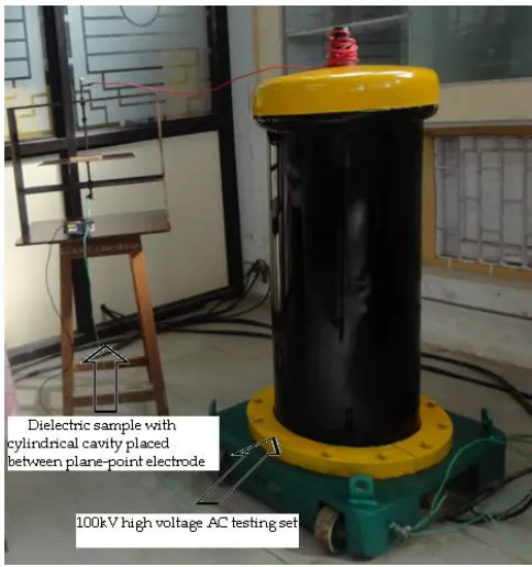
Fig.3 & Fig.4 shows overall experimental setup for detection and measurement of partial discharge. Fig.3 shows 100kV High voltage AC testing set, point-plane electrode arrangement, solid (Acrylic sheet of 100mmx100mmx5mm) dielectric sample with cylindrical cavity of 2mm diameter, discharge current sensor. By using HV control panel we can change the magnitude of high voltage applied to dielectric. With the help of meters mounted on HV panel we can monitor the magnitude of applied high voltage and leakage discharge current.
Fig.4 shows Tektronix make TDS 2014B DSO, PC with Open Choice Desktop and Tekvisa software. Current sensor senses the changes in current which can be monitored on DSO as well as PC. This current signal is used to study the partial discharge occurring at different magnitude of applied voltage.
Fig. 4: Experimental set for measurement and detection of Partial Discharge (PD)
VI. RESULTS & DICUSSION
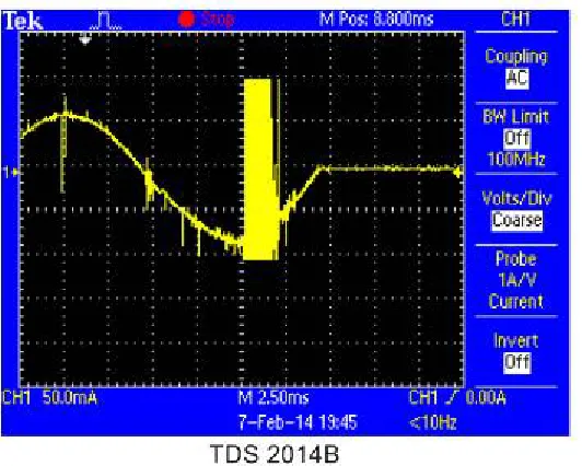
Fig.5 shows the current signal captured with the help of experimental setup on TDS 2014B DSO. The partial discharges occurring due to presence of cavity in dielectric sample are represented in the form of spikes in current waveform. Single cycle of current signal is captured.
Fig. 5: Current Signal with partial discharges captured on TDS 2014B DSO
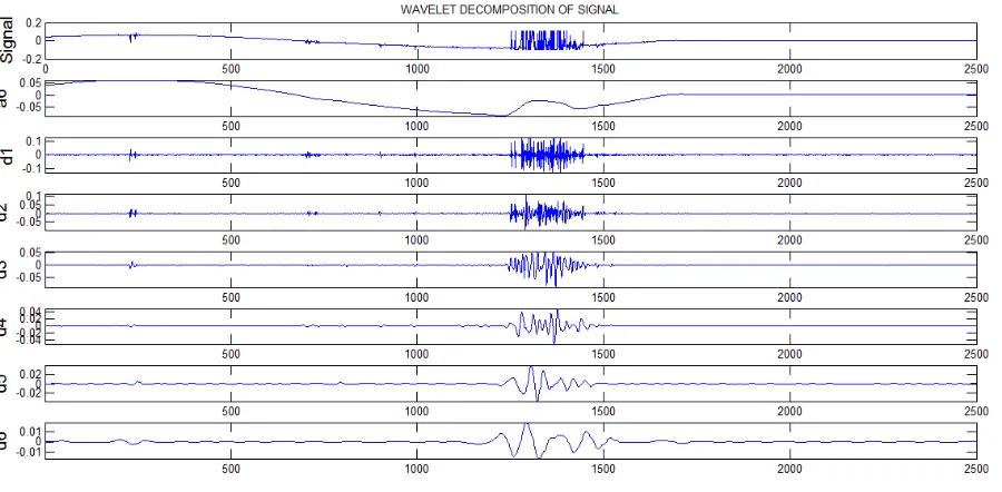
Fig.6: DWT apllied to the breakdown signal upto the level 6
Table 1 shows the statistical parameters by applying the db6 & sym6 wavelet for wavelet decomposition of captured signal at various levels.
Parameters For db6 At Level 6 For sym6 At Level 6 Mean -0.003473 -0.003473 Median 0.0032 0.0032
Mean 0.004883 0.004883 Maximum 0.103 0.103 Minimum -0.1 -0.1
Range 0.203 0.203 Standard Deviation 0.04538 0.04538
Median Abs. Dve. 0.032 0.032 Mean Abs. Dev. 0.0351 0.0351
L1 Norm. 85.44 85.44 L2 Norm. 2.275 2.275 Maximum Norm. 0.103 0.103 Table 1: Statistical Parameters of the captured breakdown waveform .
VII. CONCLUSION
REFERENCES
[1] G. C. Crichton, P. W. Karlsson and A. Pedersen, “Partial Discharges in Ellipsoidal and Spherical Voids”, IEEE Trans. on Dielectric and Electrical Insulation, Vol. 24, No. 2, pp. 335- 342, April 1989.
[2] R. J. Van Brunt, “Physics and Chemistry of partial discharges and corona”, IEEE Trans. on dielectric and Electrical Insulation, Vol. 1, No. 5, pp. 761-784, October 1994.
[3] A. Paithankar, A. D. Mokashi, “Can PD Phenomena be Analyzed by Deterministic Chaos” EIC’97, Chicago, (IEEE) Conference proceedings, pp. 283-290, 1997.
[4] N. Kolev, P. Darjanov, E. Gadjeva and D. Darjanova, “Partial Discharge Phenomena Simulation using General-purpose Analysis Program”, Proc of 6th IEEE International Conference on Conduction and Breakdown in solid Dielectrics-ICSD 98, pp. 149-152, June 22-25, Vasteras, Sweden, 1998.
[5] C. Y. Ren, Y. H. Cheng, P. Yan, Y. H. Sun, T. Shao, “Simulation of Partial Discharges in Single and Double voids Using SIMULINK”, Journal of Xi’an Jiatong University, Vol. 38, No. 10, pp. 120-122, 2004.
[6] N. Kolev, P. Darjanov, E. Gadjeva and D. Darjanova, “An approach to develop a partial discharge investigation”, Proc. of the IEEE Electrical Insulation Conference and Electrical Manufacturing and Coil Windings conference, pp. 507-510, Chicago, 1997.
[7] L. Satish, and W. S. Zaengl, “Artificial Neural Networks for recognition of 3D Partial Discharge patterns”, IEEE Trans. on Dielectrics and Electrical Insulation, Vol. 1, No. 2, pp. 265-275, April 1994.
[8] F. Gutleisch and L. Niemeyer, “Measurement and Simulation of PD in Epoxy Voids”, IEEE Transcation on Dielectrics and Electrical insulation, Vol. 2, No. 5, pp. 729-743, 1995.
[9] R. Bartnikas, “Partial Discharge their mechanism, Detection and Measurement”, IEEE Trans. Electr. Insul. Vol. 9, pp. 763-808, 2002. [10] S. Karmakar, N. K. Roy, P. Kumbhakar, “Partial Discharge Measurement of Transformer with ICT Facilities”, Third International
Conference on Power Systems, Kharagpur, India, December27 -29, 2009.
[11] S. Karmakar, N. K. Roy, P. Kumbhakar “Monitoring of high voltage power transformer Using direct Optical Partial Discharges detection technique”,journalofOptics,Vol.38,No. 4, pp.207-215, 2009.
[12] E. Kuffel, W. S. Zaengl, J. Kuffel, High Voltage Engineering: Fundamentals, Published by Elsevier, ISBN 0-7506-3634-3, second edition, 2005.
[13] M. S. Naidu and V. Kamaraju, High Voltage Engineering, New Delhi, Tata McGraw-Hill, pp. 69-85, 2004.
[14] Mu Kuen Chen and C.Y.Cheng, “Proceedings of 2008 International Symposium on Electrical Insulating Materials”, September 7-11, Yokkaichi, Mie, Japan, 2008.
[15] T. Krüger and R. Patsch, “Active Noise Reduction for Partial Discharge Measurement in the Frequency Domain”, IEEE Bologna Power Tech Conference, Bologna, Italy, June23th- 26th, 2003.
[16] G. Chen and F. Baharudin, “Partial Discharge Modeling Based on a Cylindrical Mode in Solid Dielectrics”, International Conference on Condition Monitoring and Diagnosis, China, April 21-24, 2008.