IJEDR1303054 INTERNATIONAL JOURNAL OF ENGINEERING DEVELOPMENT AND RESEARCH | IJEDR Website: www.ijedr.org | Email ID: [email protected] 264
Compact Modeled SOI MOSFET Circuits
1
Badam Suresh,
2V.S.V Srihari,
3K.Vijay Kumar
1M.Tech, VLSI Design, School of Electronics Engineering, VIT University, Vellore-India
1[email protected] , 2[email protected] , 3[email protected]
Abstract — SOI means Silicon on Insulator. This type of transistors has Silicon-Insulator-Silicon substrate which is different from
conventional MOSFET structure where metal layer is used on the top of Insulator [1, 2]. Now a days, the width of the oxide of a MOSFET is reduced from 300nm to 1.2nm and even less with scaling in technology. If it is further reduced, the leakage problems (majorly Sub-threshold Leakage) come into play [3]. In order to solve this problem and let the technology to scale further, we use a small Silicon strip on the oxide leading to next generation SOI MOSFET’s. It provides an added advantage of reduction of parasitic capacitance which improves the performance and thereby increases the speed of operation by decreasing the delay values.
In this paper, we use the BSIMSOI Model to simulate the analog circuits using EDA tools like Cadence and thereby verify the modeling of SOI MOSFET’s.
Index Terms - BSIM, Sub Threshold Leakage SOIMOSFET, SOS (silicon on sapphire).
I. INTRODUCTION
BSIMSOI stands for Berkeley short channel Insulated gate field effect Model for Silicon on Insulator. Itis a SPICE compact model for SOI (Silicon-On-Insulator) circuit design [4]. This model is formulated on top of the BSIM3 framework. The basic equation for formulating the model is similar to the equations that are used for formulating the earlier versions so that the physical nature and smoothness of older versions of BSIM are retained [5, 13]. Hence this version has compatibility with its older versions. The SOIMOSFET is clearly illustrated using the fig (1) shown below. These will also differ from the conventional MOSFETs by forming the silicon junction above the electrical insulator which are generally Sio2.The selection of the insulator is based upon the
type of application.
Fig 1 Structure of SOI MOSFET. 1. Sapphire insulator is used in place of high radio frequency applications [6]. 2. Sio2 is used in places to reduce the effects of the short channel effects.
The manufacturing process of this MOSFET implements special procedure in creating the silicon layer over the insulator .It is achieved by annealing the Silicon wafer at low temperatures [6, 7]. However, this is compatible to ordinary transistor fabrication procedure. But the only drawback to SOI technology is it contributes 10-15% high manufacturing cost due increase in cost of substrate.
The first implementation was done by the IBM in 1998.Various procedures were implemented to manufacture SOI MOSFETs such as WAFER BONDING, Seeds method. This is applied in various applications in photonics, high frequency radio applications and in microelectronic industry.
II.ENERGYBAND DIAGRAMS AND ELECTRIC FIELD DISTRIBUTION
A. Energy Band Diagrams
IJEDR1303054 INTERNATIONAL JOURNAL OF ENGINEERING DEVELOPMENT AND RESEARCH | IJEDR Website: www.ijedr.org | Email ID: [email protected] 265 Fig 2 Energy Band diagrams of (a) Bulk (b) Partially Depleted SOI MOSFET (c) Fully Depleted SOI MOSFET
B. Electric Field Distribution
The Electric Field and the potential Distribution variations of the SOI MOSFET vary according to the region of operation of the MOSFET. The region of operation of the MOSFET decides whether the back surface is in accumulation, depletion or in inversion. However the front surface is always in Inversion due to the applied input bias voltage.
The variations are shown in the figure given below in fig (3).The plots of A, B, C are shown for the Back end surface with accumulation, depletion, and inversion respectively.
Fig 3 Electric Field and Potential Distribution of SOIMOSFET
III. ADVANCEMENTS THAT LEAD TO THE INVENTION OF SOI[10]:
Now a days, Many circuits are realized using bulk models which are having low manufacturing costs, good performance , good power capability but because of more size and power consumption of other bulk models we are promising to go for SOI models. The ability of SOI models is low supply voltage and also reduction of parasitic capacitance which is very helpful to increase the speed of the digital circuits.
Multi gate-CMG, IMG, Berkeley short channel IGFET model common multi gate, BSIM independent multi gate are surface potential based models .CMGs can be built on SOI or bulks. BSIM CMG allows the user to select SOI mode or bulk mode through the addition of the body node for bulk multi gate FET. CMGs used to describe the electrical characteristics of SOI FINFETs and bulk FINFETs.
From 1990’s to till many BSIM models came into existence like bsim3, 4 conventional 6, with their special features.
There are two types of SOI transistors-partial depleted SOI and fully depleted SOI. In Partially Depleted SOI, due to the presence of high thickness silicon film on box layer the depletion layer formed below the gate oxide has many problems like floating body effects, low threshold variations with temperature. Fully Depleted SOI resolved those problems which affects due using partially depleted SOI. SOI has buried oxide layer which has many advantages mainly improvement in the switching speed and power reduction and also due to substrate bias effect it has very good operating speed.
IV.SOITECHNOLOGIES:
IJEDR1303054 INTERNATIONAL JOURNAL OF ENGINEERING DEVELOPMENT AND RESEARCH | IJEDR Website: www.ijedr.org | Email ID: [email protected] 266
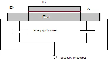
A. SOS Technology [8, 9] (silicon on sapphire)
In this technology, silicon is manufactured on sapphire layer over the substrate. By doing so, low channel electron mobility is observed in SOS MOSFETs (~230-250 /V-Sec).It improves in many areas like reducing some other parasitic capacitances due to short channel effects, lower substrate losses improving the electrical isolation. Its structure is shown in the figure (4) given below
Fig 4 Structure of SOI MOSFET.
B. BESOI (Bonded and Etch Back SOI)
It is also called as SIMOX [14]. (Separation by Implanted Oxygen). SOI is manufactured by using this process in three steps. (i)Thermally oxidizing silicon substrate wafer (A) (ii) Bonding the silicon wafer on the oxide (B) with the help of silicon fusion bonding which strengthens the bonds between Si-O-Si.
(iii) Etch back the top wafer (B) with the specified thickness.
Fig 5 Illustration of SIMOX Process
The process can be illustrated with the help of above figure 5.
C.Smart-cut [11]
It involves following steps.
1. In this process, hydrogen is implanted in the silicon substrate through thermal oxide dose as shown in the figure below. 2. Now, the wafer on the silicon (B) is bonded.
3. When the temperature is raised, the wafer A gets separated. The process can be illustrated with the help of following figure (6).
Fig 6 Illustration of Smart-cut process
D. Eltran [12]
Eltran fabrication process includes many steps like anodizing the seed wafer, installing the epitaxial Si layer on it, oxidization, bonding the silicon on the oxide, splitting the substrate ,etching it and then finally annealing it with H2.
IV. EXPERIMENTATION PROCEDURE:
In order to perform the verification of SOI MOSFET’s, the model file of the BSIM SOI is required. This model file is available in the Berkeley university website which is developed by Prof.Chenming Hu. The downloaded file includes the model files of the PMOS, NMOS, the data related to inverter’s dc and transient analysis and the output responses in Verilog A code. It also includes the construction of some circuits and the benchmark simulation of the constructed circuits. The important files we require in proceeding with our analysis are model files of PMOS and NMOS.
IJEDR1303054 INTERNATIONAL JOURNAL OF ENGINEERING DEVELOPMENT AND RESEARCH | IJEDR Website: www.ijedr.org | Email ID: [email protected] 267 of generic purpose design kit (gpdk45).After the circuit is built, launch the analog design environment for simulation .In the model libraries of the design environment, and add the BSIM SOI model files along with the gpdk45 model library. Now, simulate the circuit, generate the gate level netlist and observe the output waveforms of required interest. Thus the verification of SOIMOSFET is observed using the BSIM Model.
V. RESULTS AND DISCUSSION
The I-V characteristics of the NMOS transistor with the included nmos.mod (SOI Model file) are as follows:
Fig 7 I-V Characteristics of NMOS Transistor
The I-V characteristics of the PMOS transistor with the included pmos.mod model file (SOI Model file) are as follows:
Fig 8 I-V Characteristics of PMOS Transistor
Even though the characteristics do not vary much with respect to regular operation of normal device, there will be a significant change in the power dissipation values and the other parameters like threshold, area occupied, decreased delay etc..
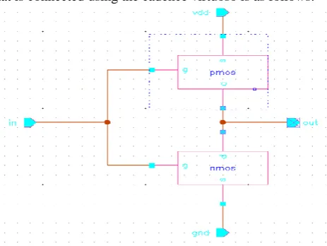
The following circuits are simulated with SOI MOSFET Transistors (Both PMOS and NMOS) The schematic of the INVERTER that is connected using the cadence virtuoso is as follows:
IJEDR1303054 INTERNATIONAL JOURNAL OF ENGINEERING DEVELOPMENT AND RESEARCH | IJEDR Website: www.ijedr.org | Email ID: [email protected] 268 Fig 10 Transient waveform of a CMOS Inverter
The Input–Output waveforms of the inverter are plotted as shown above and from the Transfer characteristics shown below, it is observed that the switching threshold voltage of the inverter is 587mV.i.e 0.58V.
Fig 11 Transfer Characterestics of CMOS Inverter The schematic of the NAND GATE that is connected using the cadence virtuoso is as follows:
Fig 12 Schematic of NAND Gate The Transient Waveform of the NAND Gate is shown below:
Fig 13 Output waveform of NAND Gate
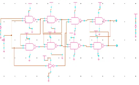
IJEDR1303054 INTERNATIONAL JOURNAL OF ENGINEERING DEVELOPMENT AND RESEARCH | IJEDR Website: www.ijedr.org | Email ID: [email protected] 269 Fig 14 Schematic of Edge Triggered D-Flip flop
The Transient Waveform of the D flipflop is shown below:
Fig 15 Output Waveform of Edge Triggered D-Flip flop During this analysis, the parameters of the transistors are as follows.
The lengths of the PMOS and NMOS Transistors are 45nm and widths of the PMOS and NMOS Transistors are 120nm. The thickness of the SOI MOSFET is observed to be 6nm. It is modeled in the model files of the transistors.
CONCLUSION:
The model files of the N-Channel and P-Channel SOIMOSFETs are successfully included into the cadence Virtuoso tool and the characteristics of PMOS and NMOS transistors, functionality of inverter, NAND gate and D-Flip-flop are verified. As the Basic Building blocks of Combinational circuits and Sequential circuits are designed using SOIMOSFETs, we can conclude that higher level circuits of any complexity can be designed using SOI MOSFETs. Therefore, the scaling of the Technology can be enabled further when the current generation MOSFETs are replaced with SOIMOSFETs. As the problem of reduction in leakage current due to thin oxide is reduced, it enables the designers to design new generation of MOSFETs like Fin-FETs where the gate of the Transistor is surrounded on all the sides of the channel so that more control of gate on the channel is provided. Hence the compact model of SOI MOSFET is verified using the BSIM model.
REFERENCES
[1]J.P. Colinge, “Romaninan Journal of Information Science and Technology ” Volume 11, Number 1,2008,3-15.
[2]Jong-Tae Park, Jean-Pierre Collinge, and Carlos H.Diaz “Pi-Gate SOI MOSFET”,IEEE Electron Device Letters,Vol.22,No.8,August 2001
[3]“Modern Semiconductor Devices for Integrated Circuits”, Chenming calvin Hu.,Pearson, 11th edition. [4]M.-C Jeng, P.M.Lee, M.M. Kuo, and C.Hu “Theory, Algorithms and User’s Guide for BSIM and SCALP”. [5]http://www.device.eecs.berkeley.edu/bsim/?page=BSIMSOI
[6]http://en.wikipedia.org/wiki/Silicon_on_insulator
[7]Vishwas Jaju, Dr. Vikram Dalal, “Silicon on Insulator Technology”,EE530,Advances inMOSFETs,Spring 2004 [8]http://www.mhprofessional.com/downloads/products/0071608486/0071608486_-culurciello_ch01.pdf
[9]James Roach, Lee-Wen Chen, Peter Clarke, and Francis M.Rotella, “Application of BSIMSOI MOSFET Model to SOS Technology”, Peregrine Semiconductor, San Diego, CA, 92121, USA.
[10]Yogesh Singh Chauhan, Sriram Venugopalan, Mohammad A. Karim, ed tc.. “BSIM-Industry Standard Compact MOSFET Models”
[11]Smart Cut guide to the Technology, the Process, the Products by George Celler and Micheal Wolf.
[12]ELTRAN; Novel SOI Wafer Technology by Takao Yonehara and Kiyofumi Sakaguchi supported by Cutting Edge 2. [13]BSIMSOI3.1 MOSFET MODEL User’s Guide,”BSIM Group, University Of California Berkeley, CA, 2003.