Approach for Lightweight ECC Design in
GF
(
p
)
Debapriya Basu Roy, Poulami Das, and Debdeep Mukhopadhyay?
Secured Embedded Architecture Laboratory (SEAL) Department of Computer Science and Engineering,
Indian Institute of Technology Kharagpur
{deb.basu.roy,debdeep}@cse.iitkgp.ernet.in,[email protected]
Abstract. Lightweight implementation of Elliptic Curve Cryptography on FPGA has been a popular research topic due to the boom of ubiq-uitous computing. In this paper we propose a novel single instruction based ultra-light ECC crypto-processor coupled with dedicated hard-IPs of the FPGAs. We show that by using the proposed single instruction framework and using the available block RAMs and DSPs of FPGAs, we can design an ECC crypto-processor for NIST curveP-256, requiring only 81 and 72 logic slices on Virtes-5 and Spartan-6 devices respectively. To the best of our knowledge, this is the first implementation of ECC which requires less than 100 slices on any FPGA device family.
Key words: Elliptic curve, Single instruction, URISC, SBN, FPGA, Hard-IPs.
1
Introduction
With the recent boom in ubiquitous computing, specially in Internet-of-Things (IoT), the need of lightweight crypto-algorithms, either at algorithmic or im-plementation level, has increased significantly. Though the researchers have pro-posed various lightweight symmetric ciphers, the most popular options for public key cryptography are RSA and Elliptic Curve Cryptography (ECC). ECC based crypto-system is being preferred over its counterpart RSA because of its won-derful property of increased security level per key bit over RSA. Any ECC based protocol or algorithm is based on underlying elliptic curve scalar multiplication whose computation is based on a number of field operations, making it compu-tationally extensive. Software implementations of ECC, running on smart cards or AVR are slow and can become performance bottleneck for many applica-tions. As an alternative, dedicated ECC-crypto processors are being built on hardware platforms like ASICs (Application Specific Integrated Circuits) and FPGAs (Field Programmable Gate Arrays).
Although ASIC implementations are faster than those based on FPGAs, FPGAs are sometimes preferred over ASIC for cryptographic applications due
?
to its inherent properties of reconfigurability, short time to market and in house security. The entire design cycle of an FPGA based system can be completed inside a single lab unlike ASIC based systems where several different parties are involved in the design cycle. Moreover, modern FPGAs with various device families provide interesting design choices to the designer. Additionally, these FPGAs are now equipped with dedicated hard IPs like DSP blocks, Block RAMs, which when properly utilized results in efficient design of dedicated ECC-based crypto-processors inGF(p) with improved timing performance and reduced area overhead.
There have been many works in the literature which focus on efficient imple-mentation of ECC crypto-processor in GF(p) on FPGAs. An overview of such implementations can be found in [1]. A lightweight ASIC design was reported in [2]. Considerably high speed designs for FPGAs can be found in [3] which is significantly faster than previous designs reported in [4, 5]. But, though the proposed design requires much less area compared to the previous designs (1715 logic slices on Virtex-4 platform for NIST P-256), it is still considerably large for lightweight applications. A fast pipelined modular multiplier for ECC field mul-tiplication was proposed in [6], whereas optimized tiling methodology targeting rectangular DSP blocks of Virtex-5 FPGA was proposed in [7]. However, both of them have considerable area overhead, hence can not be applied in lightweight applications.
A lightweight ECC algorithm for RFID tags was presented in [8] and au-thentication and ID transfer protocols based on lightweight ECC was introduced in [9]. On implementation level, authors have proposed a lightweight architecture, known as Micro-ECC, in [10]. The proposed design methodology shows signifi-cant improvement in terms ofarea-time productcompared to the previous imple-mentation [11], [12], [13]. However, Micro-ECC was implemented on Virtex-II platform which is no longer a recommended design platform by Xilinx [14]. More-over, unlike [11], [12], [13],Micro-ECC architecture does not support generalized ECC scalar multiplication on any prime field. Nevertheless, for fixed P-256 and P-224 curve, the performance of Micro-ECC outperforms other by big margin. Lightweight implementation of IPsec protocols comprising implementation of lightweight block cipher PRESENT, lightweight hash function PHOTON and ECC crypto-processor (P-160 and P-256) was presented in [15]. The ECC im-plementation requires 670 logic slices on Spartan-6 platform for NIST P-256 curve. Consequently, a lightweight architecture supporting both RSA and ECC along with some side channel countermeasure was proposed in [16]. The slice consumption of the proposed design is 1914 logic slices on Virtex-5 platform which is quite low considering dual support of RSA and ECC, provided by the design. As an alternative of standard NIST specified curves, many researchers have recommended use of Edward curve and hyper elliptic curve (HECC). Ef-ficient lightweight implementation of ECC scalar multiplication on such curves can be found in [17, 18].
in the previous works. It is well known that using a single instruction likeSBN (subtract and branch if negative),SUBLEQ (subtract and branch if the answer is negative or equal to zero), we can construct a Turing complete computer proces-sor. However, though single instruction processor can execute any arithmetical or logical operation, the execution time of some operations become so large that it can not be used in practical scenarios. Hence, a stand alone URISC processor can not be used to design computationally intensive ECC applications. How-ever, in this paper we will show that using the dedicated hard-IPs of FPGA, and with some simple modification of a URISC processor, it is possible to design an immensely lightweight and yet practical ECC architecture.
This architecture is extremely lightweight and to our best of knowledge this is the first implementation of ECC scalar multiplication which requires less than 100 slices on Virtex-5 and Spartan-6 platform. This significant reduction in slice consumption has been achieved by the lightweight architecture of single instruc-tion processor along with intensive usage of hard-IPs of the modern FPGAs. ECC scalar multiplication execution requires to compute and store multiple tempo-rary variables along with the inputs and outputs. This contributes to significant number of register usage and hence increases the slice consumption. In this pa-per, we will show an alternative design approach where we intensively use the block RAMs and reduce the slice consumption significantly. Further reduction is obtained by replacing the LUT logics with high speed DSP blocks whenever possible. The strategy of using block RAMs to reduce the slice consumption has already been applied for lightweight block ciphers like PRESENT [19], where the authors have shown that block RAM based block cipher design can be extremely lightweight resulting in more slices left for other applications.
Thus the contribution of the present paper can be listed as below:
– We propose a single instruction ECC crypto-processor for NIST P-256 curve, and analyze various challenges along with their solutions that a designer will face while applying single instruction approach in the context of lightweight implementation of ECC designs.
– We show that single instruction based ECC crypto-processor, coupled with intensive usage of block RAMs and DSP blocks, can yield extremely lightweight design for ECC scalar multiplication execution. The proposed processor re-quires less than 100 slices on both Virtex-5 and Spartan-6 family and involves thorough usage of FPGA hard-IPs.
2
Preliminaries
In this section, we will give a brief summary of ECC and single instruction processors.
2.1 Elliptic Curve Cryptography
As we have previously mentioned, elliptic curve cryptography(ECC) is a public key cryptography based on elliptic curves and finite field. Security of ECC de-pends upon the mathematical intractability of discrete logarithm of a point in elliptic curve with respect to a known base point.
ECC in finite fieldGF(p) is defined by the following equation
y2=x3+ax+b;a, b∈GF(p), b6= 0. (1)
Scalar multiplication is the most important operation in ECC for performing key agreement or digital signature schemes. Given a pointP on an elliptic curve and a scalark, scalar multiplication is computed by adding the pointP,ktimes. The basic algorithm used for scalar multiplication isDouble-and-Add algorithm, defined in Algorithm 1 in appendix A, which shows that scalar multiplication is executed by a repeated sequence of point doubling and point additions. It is advantageous to use standard projective coordinates [20] for ECC scalar multipli-cation as it requires less number of field inversion operations compared to affine coordinate system. In this paper, we have used standard projective coordinates during implementation of ECC scalar multiplication.
Now, each point addition and point doubling operation involves multiple field multiplication operation, making it most critical operation for efficient scalar multiplication execution. NIST specified curves are efficient for hardware im-plementation as modular reduction operation in those curves are simple as it involves a combination of few addition and subtraction. The fast modular re-duction algorithm for NIST P-256 is shown in appendix A.
In our proposed design, we have concentrated on the NIST P-256 curve. Nevertheless, our approach can be extended to other NIST certified curves also.
2.2 Single Instruction Processor
The concept of single instruction computer or one instruction set computer (OISC) was first proposed in [21]. It has been shown in [22] that using just a single instruction it is possible to create a Turing complete machine. The idea of applying URISC on cryptographic applications was proposed in [23]. In the similar direction, application of one instruction set computer on encrypted data computation was analyzed in [24], but in that paper the authors have investi-gated OISC in the context of homomorphic encryption and have not considered elliptic curves, which is the precise objective of the present paper.
1. ADDLEQ (Add the operands and branch if the answer is less than or equal to zero)
2. SUBLEQ (Subtract the operands and branch if the answer is less than or equal to zero)
3. SBN (Subtract the operands and branch if the answer is less than zero) 4. RSSB (Reverse subtract and skip if borrow)
5. SBNZ (Subtract the operands and branch if the answer is non-zero)
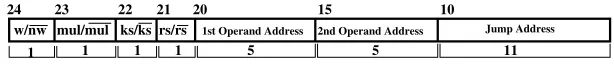
The main advantage of OISC is that we don’t need any instruction decoding mechanism, which makes the processor architecture exceptionally simple and lightweight. The instruction format of a standard OISC is shown in fig 1.
Jump Address
1st Operand Address 2nd Operand Address
Fig. 1.Instruction format of OISC
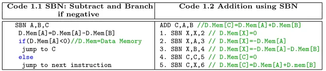
For the present work, we have chosen SBN as the single instruction. However, the proposed design strategy can be tweaked to adopt any of the above described instructions. The operation of SBN instruction is described in table 1 (code 1.1):
Table 1.SBN and Addition using SBN
Code 1.1 SBN: Subtract and Branch Code 1.2 Addition using SBN if negative
SBN A,B,C
D.Mem[A]=D.Mem[A]-D.Mem[B]
if(D.Mem[A]<0)//D.Mem=Data Memory jump to C
else
jump to next instruction
ADD C,A,B//D.Mem[C]=D.Mem[A]+D.Mem[B] 1. SBN X,X,2// D.Mem[X]=0
2. SBN X,A,3// D.Mem[X]=-D.Mem[A] 3. SBN X,B,4// D.Mem[X]=-D.Mem[A]-D.Mem[B] 4. SBN C,C,5// D.Mem[C]=0
5. SBN C,X,6// D.Mem[C]=D.Mem[A]+D.mem[B]
Using this instruction, we can execute any mathematical, logical, flow-control, memory control or load-store type of instruction. For example, in table 1 (code 1.2), we will show how to perform addition of two operands using SBN instruc-tion.
In this section we have given a brief idea about elliptic curves and OISC. In the next section, we will go into more details of OISC based on SBN instruction and will analyze it from the point of view of elliptic curve applications.
3
SBN-OISC and Elliptic Curve Scalar Multiplication
this section we will focus more on SBN-OISC in the context of ECC implemen-tation. We will identify the critical challenges that the designer will face while implementing ECC using SBN-OISC and will provide the solutions to tackle those challenges. We will first describe a stand-alone SBN-OISC processor in the next subsection
3.1 Stand-Alone SBN-OISC Processor
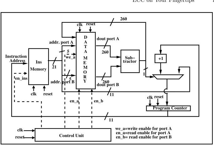
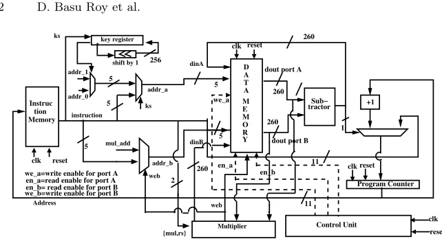
A stand-alone SBN-OISC processor is shown in fig 2. The main components of a SBN processor are characterized below:
– Instruction Memory: Instruction memory stores the instructions to be executed and can be implemented on FPGA usingblock RAMs, configured as single port ROM. In the fig 2, the instruction memory can store up to 211 number of instructions and each instruction is 21 bits wide. The format of the instruction is similar to fig 1, where address of both the operands are 5 bits wide and the length of the jump address is 11 bits.
– Data Memory: Data memory stores the final result of any computation, along with the input and all the temporary results, required during the computation. This has been implemented using block RAM, configured as true dual port RAM. The data memory has space of 32 entries, each of which are 260 bits wide. While implementing scalar multiplication in NIST P-256, the partially modular reduced output can be of size 259 bits which can be represented by 260 bits signed representation. Hence we have chosen the data path to be 260 bits wide.
– ALU: Arithmetical logical unit (ALU) of SBN-OISC contains a subtracter, which computes difference between the two inputs. If the result is negative, program counter gets updated by the jump address, specified in the instruc-tion. Otherwise, the program counter gets updated by the immediate next instruction.
The above described architecture is simple and extremely lightweight, re-quiring 66 logic slices on a Virtex-5 platform. But, as we will show in the next subsection, further optimization of ECC operation can be achieved by introduc-ing different variants of SBN instruction. In the next subsection, we will mainly concentrate on different variants of SBN instructions and will discuss how these different versions of SBN can accelerate ECC implementation.
3.2 Instruction Level Optimizations
D
T A A
M E M O R Ins
Memory
Y
Program Counter Sub−
tractor Address
Instruction
en_ins
addr. port A
addr. port B
dout port A
dout port B
Control Unit we_a
en_a clk reset
clk reset
clk
reset
reset clk
we_a=write enable for port A en_a=read enable for port A en_b= read enable for port B en_b
+1 5
5
1 260
260
11 260
11 21
Fig. 2.Architecture of SBN-OISC
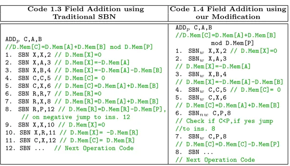
Switching off Memory Write-back When we consider traditional SBN
in-struction (SBN A, B, C), the memory location A always get updated by the result D.M em[A]−D.M em[B] (D.Mem is the data memory). But we can re-duce the required number of instruction count considerably, if we can switch off this memory write-back operation in some cases.
Let us consider a prime field addition operation. We assume that we need to add two operands stored at memory locationA andB and the modulus of the field is stored at memory locationP. In table 2 (code 1.3) shows the realization of this operation using SBN. In this case, we can see that to implement prime field addition we will require 11 SBN instructions. Now, if each SBN instruction execution takesnclock cycles, total clock cycles requirement for field operation will be 11nclock cycles.
Now, let us consider the scenario shown in table 2 (code 1.4), where we consider two variations of SBN instruction: SBNnw and SBNw.SBNw A, B, C
instruction is similar to normal SBN instruction, where memory location Aget updated by the value D.M em[A] = D.M em[A]−D.M em[B]. But in case of SBNnw A, B, C, memory locationAdoes not get updated and continue to store
the previous value. If we use a combination ofSBNwandSBNnw to implement
addition, this saving translates into significant speed up. Each point doubling operation involves 11 field addition and each point addition operation requires 7 field addition. Considering a random distribution of key value for NIST P-256 curve, containing 128 bits of zero and 128 bits of one, we can save around 256×11×4 + 128×7×4 = 14848 number of instructions, which is quite large.
Table 2.Field Addition using different SBN instructions
Code 1.3 Field Addition using Code 1.4 Field Addition using
Traditional SBN our Modification
ADDp C,A,B
//D.Mem[C]=D.Mem[A]+D.Mem[B] mod D.Mem[P] 1. SBN X,X,2 // D.Mem[X]=0
2. SBN X,A,3 // D.Mem[X]=-D.Mem[A] 3. SBN X,B,4 // D.Mem[X]=-D.Mem[A]-D.Mem[B] 4. SBN C,C,5 // D.Mem[C]= 0
5. SBN C,X,6 // D.Mem[C]=D.Mem[A]+D.Mem[B] 6. SBN R,R,7 // D.Mem[R]=0
7. SBN R,X,8 // D.Mem[R]=D.Mem[A]+D.Mem[B] 8. SBN R,P,12// D.Mem[R]=D.Mem[R]-D.Mem[P],
// on negative jump to ins. 12 9. SBN X,X,10// D.Mem[X]=0
10. SBN X,R,11// D.Mem[X]= -D.Mem[R] 11. SBN C,X,12// D.Mem[C]= D.Mem[R] 12. SBN ... // Next Operation Code
ADDp C,A,B
//D.Mem[C]=D.Mem[A]+D.Mem[B] mod D.Mem[P] 1. SBNw X,X,2 // D.Mem[X]=0 2. SBNw X,A,3
// D.Mem[X]=-D.Mem[A] 3. SBNw X,B,4
// D.Mem[X]=-D.Mem[A]-D.Mem[B] 4. SBNw C,C,5 // D.Mem[C]= 0 5. SBNw C,X,6
// D.Mem[C]=D.Mem[A]+D.Mem[B] 6. SBNnw C,P,8
// Check if C<P,if yes jump //to ins. 8
7. SBNw C,P,8
// D.Mem[C]=D.Mem[C]-D.Mem[P] 8. SBN ...
// Next Operation Code
Right Shift on SBN Processor Right shift is an important operation for
elliptic curve scalar multiplication execution as it is required during the field inversion operation. Right shift operation can be executed through SBN instruc-tion by repeated subtracinstruc-tion of the operand. For example, if we wish to right shift an operand by 1 bit position, we need to subtract the operand by 2 until the subtraction result become less than 2. Now as we are concentrating on NIST P-256 curve, the operands are typically 256 bits long, making the sequence of repeated subtraction operation extremely time consuming. On the other hand, shifter design on the FPGA has zero LUT overhead if the number of bits to be shifted are fixed. Hence, it is better if we implement right shift operation using a dedicated right shifter module instead of using SBN.
To facilitate this in our architecture, we have introduced another flag (SBNrs
andSBNrs) in our instruction format. When this flag is set, the dedicated right
shifter module reads the operand and shift it right by one bit position.
Shifting Key Register As we have stated in algorithm 1, the elliptic curve
by bit to execute scalar multiplication operation. On a standard processor this can be implemented using shift and logical AND operation. However, executing logical operations using only SBN instruction is again time consuming and hence practically infeasible.
To solve this challenge, we have used a dedicated key register, separate from the data memory shown in fig 2. Also we have introduced another flag in our instruction format (SBNks andSBNks), which when enabled will left shift the
key register by one bit. The shifted out bit from the key register will decide whether point doubling or point addition will occur.
Multiplication using SBN Field multiplication using SBN is carried out by
repeated addition. For example to multiply operand A with Operand B we need to add operandA,Btimes. Now we have already shown how to implement field addition using SBN in table 2. To complete the multiplication operation, we need to run that code, B times using a loop. Now, in the worst case scenario, the operands value in NIST P-256 curve are in the range of 2256, which makes
repeated addition implementation impractical as the loop need to run 2256times.
Hence, we can not implement field multiplication using only SBN for ECC scalar multiplication.
To solve this problem, we have designed a lightweight multiplier using DSP blocks, which acts as an external multiplier core and execute the field multipli-cation operation. However, to reset this multiplier core and to provide operand data to the multiplier we need another variant of SBN instruction, which we refer asSBNmul and SBNmul. TheSBNmul instruction resets the multiplier,
whereasSBNmul initiates the multiplication operation.The detailed description of this external multiplier core along with its interfacing with the SBN-OISC processor is provided in the next section.
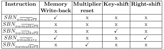
In this section, we have discussed about different variations of SBN instruc-tion, that is required for optimized ECC implementation. The list of these vari-ants can be found in table 3, where we have combined the discussed SBN instruc-tion variainstruc-tions. It should be noted that when we reset the multiplier we don’t need any memory write-back, as ALU output does not matter in that situation. Similarly when we are shifting the key register or doing the right shift operation, no memory write-back is needed.
Table 3.Different Variant of SBN Instruction
Instruction Memory Multiplier Key-shift Right-shift Write-back reset
SBNwmulksrs X x x x
SBNnwmulksrs x x x x
SBNnwmulksrs x x X x
SBNwmulksrs X x x X
To adopt these variations of SBN instructions in our architecture we also need to modify the instruction format. The modified instruction format is shown in fig 3. In the next section, we will discuss the modified SBN architecture which can support these instruction variants, along with field multiplier architecture. We would like to stress that though we are introducing different variants of SBN instruction, we are still using same ALU for each of this variant. Hence these variants are part of the same SBN instruction, with different flag values as shown in table 3.
w/nw mul/mul ks/ks rs/rs 1st Operand Address 2nd Operand Address Jump Address
5 5
1 1 1 1 11
23 22 21 20 15 10
24
Fig. 3.Modified Instruction format of SBN-OISC
4
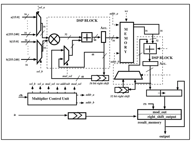
Lightweight Field Multiplier for SBN-OISC
As we have stated in the previous sections, we need to provide a dedicated light weight multiplier core to the SBN-OISC processor for efficient execution of the ECC operations. In this section we will focus on the architecture of this dedicated field multiplier and will describe the design strategies behind the proposed filed multiplier methodology.
The architecture of the field multiplier is shown in fig 4. As we can see, the architecture requires two DSP blocks, one for integer multiplication and another one for modular reduction operation. DSP blocks of Virtex-5 FPGA can sup-port 25×18 signed multiplication. It can also provide 48 bit adder/accumulator support. For our implementation, we have used DSP block as 16×16 unsigned multiplier, configured in multiply and accumulate mode. Moreover, during ad-dition operation, DSP block is configured as 32 bit adder.
We will first focus on the integer multiplier and will follow it with a discussion on the modular reduction operation.
4.1 Integer Multiplication
. . . . . . . . a[15:0] a[255:240] b[15:0] b[255:240] sel_b DSP BLOCK Acc. M E M O R Y addr_a addr_b we mul_sel
16 bit right shift
32 bit right shift
DSP BLOCK Acc. a rs 16 16 16 16 16 16 32 32 16 16 48 16 48 output mod_out right_shift_output result_memory sel_a mul_sel sel_a sel_b we 48 add/sub mod_sel addr_b addr_a
Multiplier Control Unit clk
Fig. 4.Architecture of Lightweight Field Multiplier
Let us consider a 32 bit multiplication of two operands R(= r1216+r0)
andS(=s1216+s0), divided into 16 bit words. In this scenario the addition of
partial products r1s0 and r0s1 are carried out by the operation A∗B+P as
these partial products are aligned to each other. But for the partial products which are shifted, DSP blocks operate using the second instructionA∗B+C, whereC=P >>16. The result is stored in memory of dimension 16×32 which is implemented using a block RAM configured as true dual port RAM.
R×S=
1
X
j=0
rj2j∗16×
1
X
i=0
si2i∗16 =r0s0+ (r1s0+r0s1)216+r1s1232 (2)
The integer multiplication requires 256 iteration of the DSP block, along with three clock cycles for updating the data memory. Hence the total clock cycle count for integer multiplication is 259.
4.2 Modular Reduction
D T A A M E M O R Y Program Counter Sub− tractor dout port A
we_a clk reset reset clk en_b +1 5 1
clk reset Instruc tion Memory addr_a mul_add web addr_b en_a addr_0 instruction shift by 1 addr_1
ks key register
Control Unit clk reset Address
we_a=write enable for port A en_a=read enable for port A en_b= read enable for port B we_b=write enable for port B
ks 5 5 5 5 256 260 dinA web Multiplier {mul,rs} 260 260
dout port B dinB
2
260
11
11
Fig. 5.ECC SBN-OISC Processor Architecture
needs to add operands T, S1, S2, S3.S4 and subtractD1.D2, D3, D4 from them.
We have separated the operands in 32 bit words and have used a DSP adder to execute the addition/subtraction operations. The memory produces 32 bits of output in a single clock cycle, which are added or subtracted depending on the control signaladd/sub. Like the previous DSP blocks, this one also supports two operation:P±CandC+CON CAT, whereCON CAT =P >>32 andP is the accumulator output. The first operation does the addition or subtraction of a 32 bit operand with the accumulator result, and the second operation is required to add the carry bits generated from the previous additions.
The addition and subtraction sequence of the operands are decided by the modular reduction algorithm for NIST P-256 curve, shown in appendix A. More-over, the produced result is not fully reduced but is within the range [−4p,5p] [3], wherepis the modulus of the curve. The total clock cycles required for this par-tial modular reduction operation is 68, making the total clock cycle requirement for field multiplication 327.
As we have shown in the fig 4, our architecture is also coupled with a ded-icated right shifter module. Now, when the rs flag is set high, the design will produce the right shifter output of the input operanda. Otherwise, it will pro-duce the output of the field multiplier.
5
Complete ECC SBN-OISC Processor
The ECC SBN-OISC processor is coupled with the multiplier core described in the previous section. Multiplier core is initiated by the mul flag of the in-struction. As long as themulflag is set to one, the multiplier stays in its initial stage. Once it is set low, the multiplier starts its operation and produces the partially reduced output along with signal web which indicates the completion of multiplication operation. In the stand alone SBN (fig 2), the data memory is updated only through port A. But in our case, we are also using the unused port B for writing the multiplier output into the memory. It must be noted that when thersflag is set high, the multiplier module produces right shifted output of input, available through port A.
As we have mentioned earlier, we introduced a flag ks in our instruction format for shifting the key register. Key is stored in a different register which goes though a single bit left shift when ks flag is set high. If the MSB of the key bit is one, we select the address of the memory location containing value 1 (addr 1) and pass it to the data memory. Otherwise if the MSB bit is zero, we select the memory location containing value 0 (addr 0). Once this is done we can easily switch between point doubling and addition operation depending upon the memory location passed to the data memory.
The ALU of the proposed SBN-OISC processor is a subtracter, implemented through cascaded DSP blocks. The subtraction operation requires 6 clock cycles to be completed. Instruction fetch, memory read and memory write-back require single clock cycle for each operation. Hence total clock cycle required for a single SBN instruction requires 9 clock cycles.
6
Result and Comparison
In this section we will analyze the performance of the proposed ECC SBN-OISC processor in terms of timing and area. Table 4 shows the timing and area performance of the proposed processor. As we can see, the slice count required by the design for both Virtex-5 and Spartan-6 is very small. This is achieved by in-depth usage of block-RAMs and DSP blocks. The stand alone SBN processor is itself very lightweight, and the dedicated multiplier core is designed by judicious use of DSPs and block RAMs making the slice count extremely small. The block RAMs are used to implement both data and instruction memory of the SBN-OISC processor. Moreover all the temporary storages along with control units are also implemented through block RAMs which increases the block RAM consumption, but reduces the slice count considerably. A designer can choose a budget of slices and block RAMs and then can design the ECC crypto-processor according to that budget. In this paper, we wanted to explore the limit up-to which we can reduce the slice count by increasing the block RAM usage. The result in table 4 shows that saving is significant in terms of slice usage and hence the objective of the paper is achieved.
Table 4.Area and Timing Performance of the proposed ECC SBN-OISC processor
Platform Freq. Slices LUTs Flip- DSP DSP Block- Time
(MHz) Flops for ALU for Multiplier RAM (ms)
Virtex-5 171.5 81 212 35 6 2 22 11.1
Spartan-6 156.25 72 193 35 6 2 24 12.2
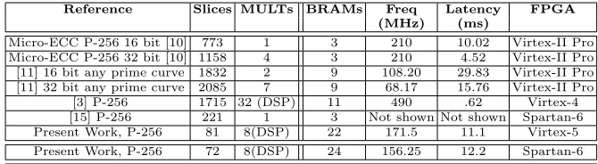
Table 5.Comparison of ECC SBN-OISC Processor with Existing Designs
Reference Slices MULTs BRAMs Freq Latency FPGA
(MHz) (ms)
Micro-ECC P-256 16 bit [10] 773 1 3 210 10.02 Virtex-II Pro
Micro-ECC P-256 32 bit [10] 1158 4 3 210 4.52 Virtex-II Pro
[11] 16 bit any prime curve 1832 2 9 108.20 29.83 Virtex-II Pro
[11] 32 bit any prime curve 2085 7 9 68.17 15.76 Virtex-II Pro
[3] P-256 1715 32 (DSP) 11 490 .62 Virtex-4
[15] P-256 221 1 3 Not shown Not shown Spartan-6
Present Work, P-256 81 8(DSP) 22 171.5 11.1 Virtex-5
Present Work, P-256 72 8(DSP) 24 156.25 12.2 Spartan-6
SBN-OISC processor shows comparable performance in terms of area and time product. But it is unfair to directly compare the proposed design and the previ-ous designs [11, 10] as they were implemented on Virtex-II pro which is extremely inefficient in comparison with Virtex-5 device family. However as FPGA devices has evolved significantly in the last decade, there is a need to update design strategies which will be efficient on these modern FPGAs. Additionally, these old FPGA families are no longer recommended for new designs by Xilinx. Motivated by these reasons, we have chosen Virtex-5 and Spartan-6 as our implementation platform, as these two FPGA family though not much new, are equipped with most of the modern hard-IPs, present in the FPGAs. The proposed processor is also much faster when compared with lightweight software libraries for ECC likeTinyECC [25]. The developed architecture is the first implementation which has reduced the slice requirement of an ECC processor to be less than 100 on Virtex-5 and Spartan-6 device family. The results shown here are obtained after post place and route analysis on Xilinx ISE.
7
Conclusion
the slice requirement decreases significantly. For Virtex-5 and Spartan-6, we have been able to achieve less than 100 slice consumption. To the best of our knowledge, this is the first implementation which has been able to achieve this feat.
A
Appendix 1
Here we will show two algorithm. The first algorithm is for ECC scalar multi-plication usingdouble and add methodology, shown in algorithm 1.
Algorithm 1: Double-and-Add Algorithm
Data: PointPand scalark=km−1, km−2, km−3...k2, k1, k0, wherekm−1= 1 Result:Q=kP
1 Q=P
2 fori=m−2to0do
3 Q= 2Q(Point Doubling)
4 ifki=1then
5 Q=Q+P(Point Addition)
Next, we will present NIST specified fast algorithm for modular reduction in NIST P-256 curve, shown in algorithm 2.
Algorithm 2: Fast Modular Reduction Algorithm for NIST P-256 Curve
Data: 512 bit productCrepresented asC=C15||C14||. . .||C0, where eachCiis
a 32 bit integer,i∈ {0,15}
Result:P =C mod P-256
1 T= (C7||C6||C5||C4||C3||C2||C1||C0) 2 S1= (C15||C14||C13||C12||C11||0||0||0)
3 S2= (0||C15||C14||C13||C12||0||0||0) 4 S3= (C15||C14||0||0||0||C10||C9||C8)
5 S4= (C8||C13||C15||C14||C13||C11||C10||C9) 6 D1= (C10||C8||0||0||0||C13||C12||C11) 7 D2= (C11||C9||0||0||C15||C14||C13||C12)
8 D3= (C12||0||C10||C9||C8||C15||C14||C13) 9 D4= (C13||0||C11||C10||C9||0||C15||C14)
10 P=T+ 2S1+ 2S2+S3+S4−D1−D2−D3−D4mod P-256
References
Microsystems, 28(56):253 – 260, 2004. Special Issue on FPGAs: Applications and Designs.
2. Lejla Batina, Nele Mentens, Kazuo Sakiyama, Bart Preneel, and Ingrid Ver-bauwhede. Low-cost elliptic curve cryptography for wireless sensor networks. In Security and Privacy in Ad-Hoc and Sensor Networks, Third European Workshop, ESAS 2006, Hamburg, Germany, September 20-21, 2006, Revised Selected Papers, pages 6–17, 2006.
3. Tim Gneysu and Christof Paar. Ultra High Performance ECC over NIST Primes on Commercial FPGAs. InIn Proceedings of CHES, pages 62–78, 2008.
4. A. Satoh and K. Takano. A Scalable Dual-field Elliptic Curve Cryptographic Processor. InIn IEEE Transactions Computers, pages 449–460, 2003.
5. G. Orlando and C. Paar. A Scalable GF(p) Elliptic Curve Processor Architec-ture for Programmable Hardware. In In Cryptographic Hardware and Embedded Systems(CHES), pages 356–371, 2001.
6. H. Alrimeih and D. Rakhmatov. Pipelined Modular Multiplier Supporting Mul-tiple Standard Prime Fields. In Application-specific Systems, Architectures and Processors (ASAP), 2014 IEEE 25th International Conference on, pages 48–56, June 2014.
7. Debapriya Basu Roy, Debdeep Mukhopadhyay, Masami Izumi, and Junko Taka-hashi. Tile Before Multiplication: An Efficient Strategy to Optimize DSP Multiplier for Accelerating Prime Field ECC for NIST Curves. In The 51st Annual Design Automation Conference 2014, DAC ’14, San Francisco, CA, USA, June 1-5, 2014, pages 177:1–177:6, 2014.
8. Cheol-Joong Kim, Sung-Yeol Yun, and Seok-Cheon Park. A Lightweight ECC Algorithm for Mobile RFID Service. InUbiquitous Information Technologies and Applications (CUTE), 2010 Proceedings of the 5th International Conference on, pages 1–6, Dec 2010.
9. Debiao He, Neeraj Kumar, Naveen Chilamkurti, and Jong-Hyouk Lee. Lightweight ECC Based RFID Authentication Integrated with an ID Verifier Transfer Protocol. Journal of Medical Systems, 38(10), 2014.
10. Michal Varchola, Tim G¨uneysu, and Oliver Mischke. MicroECC: A Lightweight Reconfigurable Elliptic Curve Crypto-processor. In 2011 International Confer-ence on Reconfigurable Computing and FPGAs, ReConFig 2011, Cancun, Mexico, November 30 - December 2, 2011, pages 204–210, 2011.
11. Jo Vliegen, Nele Mentens, Jan Genoe, An Braeken, Serge Kubera, Abdellah Touhafi, and Ingrid Verbauwhede. A Compact FPGA-based Architecture for Ellip-tic Curve Cryptography over Prime Fields. In21st IEEE International Conference on Application-specific Systems Architectures and Processors, ASAP 2010, Rennes, France, 7-9 July 2010, pages 313–316, 2010.
12. Lo’ai Ali Tawalbeh, Abidalrahman Mohammad, and Adnan Abdul-Aziz Gutub. Efficient FPGA Implementation of a Programmable Architecture for GF(p) Elliptic Curve Crypto Computations. Signal Processing Systems, 59(3):233–244, 2010. 13. Santosh Ghosh, Monjur Alam, Dipanwita Roy Chowdhury, and Indranil Sen
Gupta. Parallel Crypto-devices for GF(P) Elliptic Curve Multiplication Resis-tant Against Side Channel Attacks. Comput. Electr. Eng., 35(2):329–338, March 2009.
14. Xilinx Inc. Virtex-II and Virtex-II Pro X FPGA User Guide, February 14 2011. 15. Benedikt Driessen, Tim G¨uneysu, Elif Bilge Kavun, Oliver Mischke, Christof Paar,
16. Christopher P¨opper, Oliver Mischke, and Tim G¨uneysu. MicroACP - A Fast and Secure Reconfigurable Asymmetric Crypto-Processor - -Overhead Evaluation of Side-Channel Countermeasures-. In Reconfigurable Computing: Architectures, Tools, and Applications - 10th International Symposium, ARC 2014, Vilamoura, Portugal, April 14-16, 2014. Proceedings, pages 240–247, 2014.
17. Andr´e Himmighofen, Bernhard Jungk, and Steffen Reith. On a FPGA-based Method for Authentication using Edwards Curves. In2013 8th International Work-shop on Reconfigurable and Communication-Centric Systems-on-Chip (ReCoSoC), Darmstadt, Germany, July 10-12, 2013, pages 1–7, 2013.
18. Junfeng Fan, Lejla Batina, and Ingrid Verbauwhede. Light-weight Implementation Options for Curve-Based Cryptography: HECC is also ready for RFID. InICITST, pages 1–6. IEEE, 2009.
19. E.B. Kavun and T. Yalcin. RAM-Based Ultra-Lightweight FPGA Implementa-tion of PRESENT. InReconfigurable Computing and FPGAs (ReConFig), 2011 International Conference on, pages 280–285, Nov 2011.
20. Darrel Hankerson, Alfred J. Menezes, and Scott Vanstone.Guide to Elliptic Curve Cryptography. Springer-Verlag New York, Inc., Secaucus, NJ, USA, 2003. 21. Farhad Mavaddat and Behrooz Parhamt. URISC: The Ultimate Reduced
Instruc-tion Set Computer. International Journal of Electrical Engineering Education, 25:327–334, 1988.
22. William F. Gilreath and Phillip A. Laplante. Computer Architecture : a Minimal-ist Perspective. The Springer International Series in Engineering and Computer Science. Springer US, 2003.
23. David Naccache. Is Theoretical Cryptography Any Good in Practice? CHES 2010. 24. Nektarios Georgios Tsoutsos and Michail Maniatakos. Investigating the Appli-cation of One Instruction Set Computing for Encrypted Data Computation. In Security, Privacy, and Applied Cryptography Engineering - Third International Conference, SPACE 2013, Kharagpur, India, October 19-23, 2013. Proceedings, pages 21–37, 2013.