How to Efficiently Evaluate RAM Programs
with Malicious Security
Arash Afshar
∗Zhangxiang Hu
†Payman Mohassel
‡Mike Rosulek
†January 29, 2015
Abstract
Secure 2-party computation (2PC) is becoming practical for some applications. However, most ap-proaches are limited by the fact that the desired functionality must be represented as a boolean circuit. In response, random-access machines (RAM programs) have recently been investigated as a promising alternative representation.
In this work, we present the first practical protocols for evaluating RAM programs with security against malicious adversaries. A useful efficiency measure is to divide the cost of malicious-secure evalu-ation offby the cost of semi-honest-secure evaluation off. Our RAM protocols achieve ratios matching the state of the art for circuit-based 2PC. For statistical security 2−s, our protocol without preprocessing achieves a ratio of s; our online-offline protocol has a pre-processing phase and achieves online ratio
∼2s/logT, whereT is the total execution time of the RAM program.
To summarize, our solutions show that the “extra overhead” of obtaining malicious security for RAM programs (beyond what is needed for circuits) is minimal and does not grow with the running time of the program.
1
Introduction
General secure two-party computation (2PC) allows two parties to perform “arbitrary” computation on their joint inputs without revealing any information about their private inputs beyond what is deducible from the output of computation. This is an extremely powerful paradigm that allows for applications to utilize sensitive data without jeopardizing its privacy.
From a feasibility perspective, we know that it is possible to securely compute any function, thanks to seminal results of [Yao82,GMW87]. The last decade has also witnessed significant progress in design and implementation of more practical/scalable secure computation techniques, improving performance by orders of magnitude and enabling computation of circuits with billions of gates.
These techniques, however, are largely restricted to functions represented as Boolean or arithmetic cir-cuits, whereas the majority of applications we encounter in practice are more efficiently captured using random-access memory (RAM) programs that allow constant-time memory lookup. Modern algorithms of practical interest (e.g., binary search, Dijkstra’s shortest-paths algorithm, and the Gale-Shapely stable matching algorithm) all rely on fast memory access for efficiency, and suffer from major blowup in running time otherwise. More generally, a circuit computing a RAM program with running timeT requires Θ(T2)
gates in the worst case, making it prohibitively expensive (as a general approach) to compile RAM programs into a circuit and then apply known circuit 2PC techniques.
A promising alternative approach uses the building block of oblivious RAM, introduced by Goldreich and Ostrovsky [GO96]. ORAM is an approach for making a RAM program’s memory access pattern input-oblivious while still retaining fast (polylogarithmic) memory access time. Recent work in 2PC has begun to investigate direct computation of ORAM computations as an alternative to RAM-to-circuit compilation [GKK+12,LO13,KS14,GHL+14,LHS+14]. These works all follow the same general approach of evaluating a
∗University of Calgary. [email protected]
†Oregon State University.{huz,rosulekm}@eecs.oregonstate.edu. Supported by NSF award CCF-1149647. ‡Yahoo Labs.
sequence of ORAM instructions using traditional circuit-based 2PC phases. More precisely, they use existing circuit-based MPC to (1) initialize and setup the ORAM, a one-time computation with cost proportional to the memory size, (2) evaluate the next-instruction circuit which outputs “shares” of the RAM program’s internal state, the next memory operations (read/write), the location to access, and the data value in case of a write. All of these existing solutions provide security only against semi-honest adversaries.
Challenges for malicious-secure RAM evaluation. It is possible to take a semi-honest secure protocol for RAM evaluation (e.g., [GKK+12]) and adapt it to the malicious setting using standard techniques. Doing
so na¨ıvely, however, would result in several major inefficiencies that are avoidable. We point out three significant challenges for efficient, malicious-secure RAM evaluation:
1: Integrity and consistency of state information, by which we mean both the RAM’s small internal state and its large memory both of which are passed from one CPU step to the next. A natural approach for handling internal state is to have parties hold secret shares of the state (as in [GKK+12]), which they provide as input to a secure evaluation of the next-instruction circuit. Using standard techniques for malicious-secure SFE, it would incur significant overhead in the form of oblivious transfers and consistency checks to deal with state information as inputs to the circuit.
A natural approach suitable for handling RAM memory is to evaluate an Oblivious RAM that encrypts its memory contents. In this approach, the parties must evaluate a next-instruction circuit that includes both encryption and decryption sub-circuits. Evaluating a block cipher’s circuit securely against malicious adversaries is already rather expensive [KsS12], and this approach essentially asks the parties to do so at every time-step, even when the original RAM’s behavior is non-cryptographic. Additional techniques are needed to detect any tampering of data by either participant, such as computing/verifying a MAC of each memory location access inside the circuit or computing a “shared” Merkle-tree on top of the memory in order to check its consistency after each access. All these solutions incur major overhead when state is passed or memory is accessed and are hence prohibitively expensive (see AppendixAfor a concrete example).
2: Compatibility with batch execution and input-recovery techniques. In a secure computation, every input bit must be “touched” at some point. Oblivious RAM programs address this with a pre-processing phase that “touches” the entire (large) RAM memory, after which the computation need not “touch” every bit of memory. Since an offline phase is already inevitable for ORAMs, we would like to use such a phase to further increase the efficiency of the online phase of the secure evaluation protocol. In particular, recent techniques of [HKK+14,LR14] suggest that pre-processing/batching garbled circuits can lead to significant efficiency improvement for secure evaluation of circuits. The fact that the ORAM next-instruction circuits are used at every timestep and are known a priorimakes the use of batch execution techniques even more critical.
Another recent technique, called input-recovery [Lin13], reduces the number of garbled circuits in cut-and-choose by a factor of 3 by only requiring that at least one of the evaluated circuits is correct (as opposed to the majority). This is achieved by running an input-recovery step at the end of computation that recover’s the garbler’s private input in case he cheats in more than one evaluated circuit. The evaluator then uses the private input to do the computation on his own. A natural applications of this technique in case of RAM programs, would require running the input-recovering step after every timestep which would be highly inefficient (see AppendixAfor a concrete example).
3: Run-time dependence. The above issues are common to any computation that involves persistent, secret internal state across several rounds of inputs/outputs (any so-calledreactivefunctionality). RAM pro-grams present an additional challenge, in that only part of memory is accessed at each step, and furthermore these memory locations are determinedonly at run-time. In particular, it is non-trivial to reconcile run-time data dependence with offline batching optimizations.
Hence, instead of secret-sharing the internal state of the RAM program between the parties, we simply “re-use” the garbled wire labels from the output of one circuit into the input of the next circuit. These wire labels already inherit the required authenticity properties, so no oblivious transfers or consistency checks are needed.
Similarly, we also encode the RAM’s memory via wire labels. When the RAM reads from memory location `, we simply reuse the appropriate output wire labels from the most recent circuit to write to location`(not necessarily the previous instruction, as is the case for the internal state). Since the wire labels already hide the underlying logical values, we only require an oblivious RAM that hides the memory access pattern and
notthe contents of memory. More concretely, this means that we do not need to add encryption/decryption and MAC/verify circuitry inside the circuit that is being garbled or perform oblivious transfers on shared intermediate secrets. Importantly, if the RAM program being evaluated is “non-cryptographic” (i.e., has a small circuit description) then the circuits garbled at each round of our protocols will be small.
Of course, it is a delicate task to make these intuitive ideas work with the state of art techniques for cut-and-choose. We present two protocols, which use different approaches for reusing wire labels.
The first protocol uses ideas from the LEGO paradigm [NO09,FJN+13] for 2PC and other recent works on batch-preprocessing of garbled circuits [HKK+14,LR14]. The idea behind these techniques is to generate all the necessary garbled circuits in an offline phase (before inputs are selected), open and check a random subset, and randomly assign the rest into buckets, where each bucket corresponds to one execution of the circuit. But unlike the setting of [HKK+14, LR14], where circuits are processed for many independent
evaluations of a function, we have the additional requirement that the wire labels for memory and state data should be directly reused between various garbled circuits. Since we cannot know which circuits must have shared wire labels (due to random assignment to buckets and run-time memory access pattern), we use the “soldering” technique of [NO09,FJN+13] that directly transfers garbled wire labels from one wire
to another, after the circuits have been generated. However, we must adapt the soldering approach to make it amenable to soldering entire circuits as opposed to soldering simple gates as in [NO09, FJN+13]. For a
discussion of subtle problems that arise from a direct application of their soldering technique, see Section3. Our second approach directly reuses wire labels without soldering. As a result, garbled circuits cannot be generated offline, but the scheme does not require the homomorphic commitments required for the LEGO soldering technique. At a high level, we must avoid having the cut-and-choose phase reveal secret wire labels that are shared in common with other garbled circuits. The technique recently proposed in [MGFB14] allows us to use a single choose for all steps of the RAM computation (rather than independent cut-and-choose steps for each time step), and further hide the set of opened/evaluated circuits from the garbler using an OT-based cut-and-choose [KMR12,KsS12]. We observe that this approach is compatible with the state of the art techniques for input-consistency check [MR13, sS13].
We also show how to incorporate the input-recovery technique of [Lin13] for reducing the number of circuits by a factor of three. The naive solution of running the cheating recovery after each timestep would be prohibitively expensive since it would require running a malicious 2PC for the cheating recovery circuit (and the corresponding input-consistency checks) at every timestep. We show a modified approach that only requires a final cheating recovery step at the end of the computation.
Based on some concrete measurements in Appendix A (see table1), the “extra overhead” of achieving malicious security for RAM programs (i.e. the additional cost beyond what is needed for malicious security of the circuits involved in the computation), is at least an order of magnitude smaller than the naive solutions and this gap grows as the running time of the RAM program increases.
Related work. Starting with seminal work of [Yao86,GMW87], the bulk of secure multiparty computation protocols focus on functions represented as circuits (arithmetic or Boolean). More relevant to this work, there is over a decade’s worth of active research on design and implementation of practical 2PC protocols with malicious security based on garbled circuits [MF06,KS06,LP07,LP11,sS11,sS13, Lin13,HKE13,MR13], based on GMW [NNOB12], and based on arithmetic circuits [DPSZ12].
The work on secure computation of RAM programs is much more recent. [GKK+12] introduces the idea
of using ORAM inside a Yao-based secure two-party computation in order to accommodate (amortized) sublinear-time secure computation. The work of [LO13, GHL+14] study non-interactive garbling schemes
of [DPSZ12], hence extending these ideas to the multiparty case, and implementing various oblivious data-structures. SCVM [LHS+14] and Obliv-C [Zah14] provide frameworks (including programming languages) for secure computation of RAM programs that can be instantiated using different secure computation RAM programs on the back-end. The above work all focus on the semi-honest adversarial model. To the best of our knowledge, our work provides the first practical solution for secure computation of RAM program with malicious security. Our constructions can be used to instantiate the back-end in SCVM and Obliv-C with malicious security.
2
Preliminaries
2.1
(Oblivious) RAM Programs
A RAM program is characterized by a deterministic circuit Π and is executed in the presence of memory M. The memory is an array ofblocks, which are initially set to 0n. An execution of the RAM program Π on inputs (x1, x2) with memoryM is given by:
RAMEval(Π, M, x1, x2)
st:=x1kx2k0n;block:= 0n; inst:=⊥
do untilinst has the form (halt, z):
block:= [ifinst= (read, `) thenM[`] else 0n] r← {0,1}n; (st,inst,block) := Π(st,block, r) ifinst= (write, `) thenM[`] :=block
outputz
Oblivious RAM, introduced in [GO96], is a technique for hiding all information about a RAM program’s memory (both its contents and the data-dependent access pattern). Our constructions require a RAM program that hides only the memory access pattern, and we will use other techniques to hide thecontentsof memory. Throughout this work, when we use the term “ORAM”, we will be referring to this weaker security notion. Concretely, such an ORAM can often be obtained by taking a standard ORAM construction (e.g., [SvDS+13,CP13]) and removing the steps where it encrypts/decrypts memory contents.
Define I(Π, M, x1, x2) as the random variable denoting the sequence of values taken by theinstvariable
in RamEval(Π, M, x1, x2). Our precise notion of ORAM security for Π requires that there exist a simulatorS
such that, for allx1,x2and initially emptyM, the outputS(1λ, z) is indistinguishable fromI(Π, M, x1, x2),
wherez is the final output of the RAM program on inputsx1, x2.
2.2
Garbling Schemes
In this section we adapt the abstraction of garbling schemes [BHR12b] to our needs. Our 2PC protocol constructions re-use wire labels between different garbled circuits, so we define a specialized syntax for garbling schemes in which the input and output wire labels are pre-specified.
We represent a set of wire labelsW as am×3 array. Wire labelsW[i,0] andW[i,1] denote the two wire labels associated with some wire i. We employ the point-permute optimization [PSSW09], so we require
lsb(W[i, b]) =b. The value W[i,2] is a single-bit translation bit, so thatW[i, W[i,2]] is the wire label that encodesfalsefor wirei. For shorthand, we use τ(W) to denote them-bit stringW[1,2]· · ·W[m,2].
We require the garbling scheme to have syntax F ← Garble(f, E, D) where f is a circuit, E and D represent wire labels as above.
For v ∈ {0,1}m, we define W|
v = (W[1, v1], . . . , W[m, vm]), i.e., the wire labels with select bits v. We also defineW|∗
x:=W|x⊕τ(W), i.e., the wire labels corresponding totruth valuesx. The correctness condition
we require for garbling is that, for allf, x, and valid wire label descriptionsE,D, we have:
Eval(Garble(F, E, D), E|∗x) =D|∗f(x)
IfY denotes a vector of output wire labels, then it can be decoded to a plain output vialsb(Y)⊕τ(D), where
µ∈ {0,1}m is a mask value, then revealing (µ, τ(D)∧µ) allows the evaluator to learn only the output bits for whichµi= 1.
LetWdenote the uniform distribution ofm×3 matrices of the above form (wire labels with the constraint on least-significant bits described above). Then the security condition we need is that there exists an efficient simulatorS such that for allf, x, D, the following distributions are indistinguishable:
Real(f, x, D): E← W
F ←Garble(f, E, D)
return (F, E|∗x)
SimS(f, x, D): E← W
F ← S(f, E|∗
x, D|∗f(x))
return (F, E|∗ x)
To understand this definition, consider an evaluator who receives garbled circuit F and wire labelsE|∗ x which encode its inputx. The security definition ensures that the evaluator learns no more than the correct output wiresD|∗
f(x).
Consider what happens when we apply this definition withD chosen from W and against an adversary who is given only partial decoding information (µ, τ(D)∧µ).1 Such an adversary’s view is then independent of f(x)∧µ. This gives us a combination of theprivacyandobliviousnessproperties of [BHR12b]. Furthermore, the adversary’s view is independent of the complementary wire labelsD|∗
f(x), except possibly in their least
significant bits (by the point-permute constraint). So the other wire labels are hard to predict, and we achieve anauthenticityproperty similar to that of [BHR12b].2
Finally, we require that it be possible to efficiently determine whetherF is in the range ofGarble(f, E, D), given (f, E, D). For efficiency improvements, one may also reveal a seed which was used to generate the randomness used inGarble.
These security definitions can be easily achieved using typical garbling schemes used in practice (e.g., [KS08]). We note that the above arguments hold even when the distribution W is slightly different. For instance, when using the Free-XOR optimization [KS08], wire label matrices E and D are chosen from a distribution parameterized by a secret ∆, whereE[i,0]⊕E[i,1] = ∆ for alli. This distribution satisfies all the properties ofW that were used above.
Conventions for wire labels. We exclusively garble the ORAM circuit which has its inputs/outputs partitioned into several logical values. When W is a description of input wire labels for such a circuit, we
letst(W), rand(W), block(W) denote the submatrices of W corresponding to the incoming internal state,
random tape, and incoming memory block. When W describes output wires, we use st(W), inst(W) and
block(W) to denote the outgoing internal state, output instruction (read/write/halt, and memory location),
and outgoing memory data block. We use these functions analogously for vectors (not matrices) of wire labels.
2.3
(XOR-Homomorphic) Commitment
In addition to a standard commitment functionalityFcom, one of our protocols requires an XOR-homomorphic
commitment functionality Fxcom. This functionality allows P1 to open the XOR of two or more commited
messages without leaking any other information about the individual messages. The funcionality is defined in Figure1. Further details, including an implementation, can be found in [FJN+13].
3
Batching Protocol
3.1
High-level Overview
Roughly speaking, the LEGO technique of [NO09,FJN+13] is to generate a large quantity of garbled gates, perform a cut-and-choose on all gates to ensure their correctness, and finally assemble the gates together into
1Our definition applies to this case, since a distinguisher for the above two distributions is allowed to know D which
parameterizes the distributions.
2We stress that the evaluatorcan indeed decodethe garbled output (usingτ(D) and the select bits), yetcannot forgevalid
The functionality is initialized with internal valuei= 1. It then repeatedly responds to com-mands as follows:
• On input (commit, m) fromP1, store (i, m)
internally, set i := i + 1 and output (committed, i) to both parties.
• On input (open, S) from P1, where S is a
set of integers, for each i ∈ S find (i, mi) in memory. If for some i, no such mi exists, send ⊥ to P2. Otherwise, send
(open, S,L
i∈Smi) toP2.
Figure 1: XOR-homomorphic commitment functionalityFxcom.
a circuit which can tolerate a bounded number of faulty gates (since the cut-and-choose will not guarantee that all the gates are correct). More concretely, with sN gates and a cut-and-choose phase which opens half of them correctly, a statistical argument shows that permuting the remaining gates into buckets of size O(s/logN) each ensures that each bucket contains a majority of correct gates, except with negligible probability ins.
For each gate, the garbler provides a homomorphic commitment to its input/output wire labels, which is also checked in the cut and choose phase. This allows wires to be connected on the fly with a technique called soldering. A wire with labels (w0, w1) (here 0 and 1 refer to the public select bits) can be soldered
to a wire with labels (w00, w10) as follows. Ifw0 and w00 both encode the same truth value, then decommit
to ∆0 = w0⊕w00 and ∆1 = w1⊕w01. Otherwise decommit to ∆0 = w0⊕w10 and ∆1 = w1⊕w00. Then
when an evaluator obtains the wire labelwb on the first wire,wb⊕∆b will be the correct wire label for the second wire. To prove that the garbler hasn’t inverted the truth value of the wires by choosing the wrong case above, she must also decommit to the XOR of each wire’stranslationbit (i.e.,β⊕β0 wherew
β andw0β0 both encode false).
Next, an arbitrary gate within each bucket is chosen as the head. For each other gate, we solder its input wires to those of the head, and output wires to those of the head. Then an evaluator can transfer the input wire labels to each of the gates (by XORing with the appropriate solder value), evaluate the gates, and transfer the wire labels back. The majority value is taken to be the output wire label of the bucket. The cut-and-choose ensures that each bucket functions as a correct gate, with overwhelming probability. Then the circuit can be constructed by appropriately soldering together the buckets in a similar way.
For our protocol we use a similar approach but work with buckets of circuits, not buckets of gates. Each bucket evaluates a single timestep of the RAM program. To transfer RAM memory and internal state between timesteps, we solder wires together appropriately (i.e., state input of timet soldered to state output of timet−1; memory-block inputtsoldered to memory-block output of the previous timestep that wrote to the desired location). Additionally, the approach of using buckets also saves an asymptotic logT factor in the number of circuits needed for each timestep (i.e., the size of the buckets), whereT is the total running time of the ORAM, a savings that motivates similar work on batch pre-processing of garbled circuits [HKK+14, LR14].
We remark that our presentation of the LEGO approach above is a slight departure from the original papers [NO09,FJN+13]. In those works, all gates were garbled using Free XOR optimization, wherew
0⊕w1
is a secret constant shared on all wires. Hence, we have only one “solder” value w0⊕w00 =w1⊕w10. If
the sender commits to only the “false” wire label of each wire, then the sender is prevented from inverting the truth value while soldering (“false” is always mapped to “false”). However, to keep the offsetw0⊕w1
secret, only one of the 4 possible input combinations of each gate can be opened in the cut-and-choose phase. The receiver has only a 1/4 probability of identifying a faulty gate. This approach does not scale to a cut-and-choose of entire circuits, where the number of possible input combinations is exponential. Hence our approach of forgoing common wire offsetsw0⊕w1between circuits and instead committing to the translation
GC(1)
GC(2)
GC(3)
maj
E(1) D(1)
E(2) D(2)
E(3) D(3)
∆(1→2)
∆(1→3)
∆(2→1)
∆(3→1)
Figure 2: Illustration ofMkBucket(B={1,2,3},hd= 1).
detect faulty circuits with probability 1, not 1/4.
Back to our protocol, P1 generatesO(sT /logT) garblings of the ORAM’s next-instruction circuit, and
commits to the circuits and their wire labels. P2 chooses a random half of these to be opened and aborts if
any are found to be incorrect.
For each timestep t, P2 picks a random subset of remaining garbled circuits and the parties assemble
them into a bucket Bt (this is the MkBucket subprotocol) by having P1 open appropriate XORs of wire
labels, as described above. We can extend the garbled-circuit evaluation functionEvalto EvalBucketusing the same syntax. ThenEvalBucketinherits the correctness property ofEvalwith overwhelming probability, for each of the buckets created in the protocol.
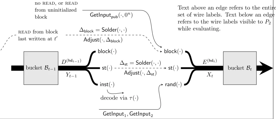
After a bucket is created, P2 needs to obtain garbled inputs on which to evaluate it. See Figure 3 for
an overview. LetXtdenote the vector of input wire labels to bucketBt. We useblock(Xt),st(Xt),rand(Xt) to denote the sets of wire labels for the input memory block, internal state, and shares of random tape, respectively. The simplest wire labels to handle are the ones for internal state, as they always come from the previous timestep. We solder the output internal state wires of bucketBt−1 to the input internal state
wires of bucket Bt. Then if Yt−1 were the output wire labels for bucket Bt−1 by P2, we obtain st(Xt) by adjustingst(Yt−1) according to the solder values.
If the previous memory instruction was a readof a location that was last written to at time t0, then we need to solder the appropriate output wires from bucketBt0 to the corresponding input wires ofBt. P2 then obtainsblock(Xt) by adjusting the wire labelsblock(Yt0) according to the solder values. If the previous memory instruction was a read of an uninitialized block, or a write, then P1 simply opens these input
wire labels to all zero values (seeGetInputpub).
To obtain wire labelsrand(Xt), we haveP1open wire labels for its shares (GetInput1) and haveP2obtain
its wire labels via a standard OT (GetInput2).
At this point, P2 can evaluate the bucket (EvalBucket). LetYtdenote the output wire labels. P1 opens
the commitment to their translation values, soP2can decode and learn these outputs of the circuit. P2sends
these labels back toP1, who verifies them for authenticity. Knowing only the translation values and not the
entire actual output wire labels,P2 cannot lie about the circuit’s output except with negligible probability.
3.2
Detailed Protocol Description
Let Π be the ORAM program to be computed. Define ˜Π(st,block,inp1,inp2,1, . . . ,inp2,n) = Π(st,block,inp1,
L
iinp2,i). Looking ahead, during the first timestep, the parties will provide inp1 =x1 andinp2 =x2, while in
subse-quent timesteps they input their sharesr1 andr2 of the RAM program’s randomness. P2’s input is further
secret shared to prevent a selective failure attack on bothx2 and his random input r2. We first define the
following subroutines / subprotocols:
protSolder(A, A0) //A,A0 are wire labels descriptions P1opensFxcom-commitments toτ(A) andτ(A0)
so thatP2 receivesτ=τ(A)⊕τ(A0)
bucketBt−1 st(·) bucketBt
block(·)
inst(·)
st(·)
block(·)
rand(·) D(hdt−1)
Yt−1
E(hdt)
Xt ∆st=Solder(·,·)
Adjust(·,∆st)
readfrom block last written att0
∆block=Solder(·,·)
Adjust(·,∆block)
noread, or read from uninitialized
block GetInputpub(·,0n)
decode viaτ(·)
GetInput1,GetInput2
Text above an edge refers to the entire set of wire labels. Text below an edge refers to the wire labels visible to P2
while evaluating.
Figure 3: Overview of soldering and evaluation steps performed in the online phase.
P1 opensFxcom-commitments toA[i, b] andA0[i, τi⊕b] so thatP2 receives ∆[i, b] =A[i, b]⊕A0[i, τi⊕b] return ∆
protMkBucket(B,hd) //Bis a set of indices for eachj ∈ B \ {hd}:
∆(hd→j)=Solder(E(hd), E(j))
∆(j→hd)=Solder(D(j), D(hd))
∆(hd→hd):= all zeroes // for convenience
funcAdjust(X,∆) // X is a vector of wire labels
for eachi do ˜X[i] =X[i]⊕∆[i,lsb(X[i])] return ˜X
funcEvalBucket(B, X,hd) for eachj in B:
˜
Xj =Adjust(X,∆(hd→j)))
Yj=Adjust(Eval(GC(j),X˜j),∆(j→hd)) return the majority element of{Yj}j∈B
protGetInputpub(A, x) //Adescribes wire labels; xpublic
P1opens commitments ofA|∗x; call the resultX P1opens commitments ofτ(A)
P2aborts iflsb(X)6=τ(A)⊕x; else returnsX
protGetInput1(A, x) //Adescribes wire labels;P1 holdsx
P1opens commitments ofA|∗x; return these values
protGetInput2(A, x) //Adescribes wire labels;P2 holdsx
for each positioni inA, parties invoke an instance ofFot:
P1 uses input (A[i, A[i,2]], A[i,1⊕A[i,2]])
P2 uses inputxi
P2 stores the output asX[i]
We now describe the main protocol for secure evaluation of Π. We letsdenote a statistical security parameter, andT denote an upper bound on the total running time of Π.
1. [Pre-processing phase] Circuit garbling: P1andP2agree on the total numberN =O(sT /logT)
of garbled circuits to be generated. Then, for each circuit indexi∈ {1, . . . , N}:
(a) P1 chooses random input/output wire label descriptionsE(i),D(i)and commits to each of these
values component-wise underFxcom.
(b) P1 computesGC(i)=Garble( ˜Π, E(i), D(i)) and commits toGC(i)underFcom.
2. [Pre-processing phase] Cut and choose: P2randomly picks a subsetScof{1, . . . , N}of sizeN/2 and sends it toP1. Sc will denote the set of check circuits andSe={1, . . . , N} \Sc will denote the set of evaluation circuits. For check circuit indexi∈Sc:
(a) P1 opens the commitments ofE(i),D(i), and GC(i).
(b) P2 checks thatGC(i)∈Garble( ˜Π, E(i), D(i)); if not,P2 aborts.
3. Online phase: For each timestept:
(a) Bucket creation: P2chooses a random subset ofBtofSeof size Θ(s/logT) and a random head circuithdt∈ Bt. P2 announces them toP1. Both parties setSe:=Se\ Bt.
(b) Garbled input: randomness: P1 chooses random r1 ← {0,1}n, and P2 chooses random
r2,1, . . . , r2,n← {0,1}n. P2 sets
rand1(Xt) =GetInput1(rand1(E(hdt)), r1)
rand2(Xt) =GetInput2(rand2(E(hdt)), r2,1· · ·r2,n)
(c) Garbled input: state: Ift >1 then the parties execute:
∆st=Solder(st(D(hdt−1)),st(E(hdt)))
andP2 setsst(Xt) :=Adjust(st(Yt−1),∆st).
Otherwise, in the first timestep, let x1 and x2 denote the inputs ofP1 andP2, respectively. For
input wire labels W, let st1(W),st2(W),st3(W) denote the groups of the internal state wires
corresponding to the initial state x1kx2k0n. To prevent selective abort attacks, we must have
P2 encode his input as n-wise independent shares, as above. P2 chooses randomr2,1, . . . , r2,n ∈
{0,1}n such thatPn
i r2,i=x2, and sets:3
st(Xt) =GetInput1(st1(E(hdt)), x1)
kGetInput2(st2(E(hdt)), r2,1· · ·r2,n)
kGetInputpub(st3(E(hdt)),0n)
(d) Garbled input: memory block: If the previous instructioninstt−1= (read, `) and no previous
(write, `) instruction has happened, or if the previous instruction was not a read, then the
parties doblock(Xt) =GetInputpub(block(E(hdt)),0n).
Otherwise, ifinstt−1= (read, `) andt0 is the largest time step withinstt0 = (write, `), then the parties execute:
∆block=Solder(block(D(hdt0)),block(E(hdt)))
ThenP2 setsblock(Xt) :=Adjust(block(Yt0),∆block).
3We are slightly abusing notation here. More precisely, the parties are evaluating a slightly different circuit ˜Π in the first
(e) Construct bucket: P1 andP2run subprotocolMkBucket(Bt,hdt) to assemble the circuits. (f) Circuit evaluation: For each i∈ Bt,P1 opens the commitment toGC(i) and toτ(inst(D(i))).
P2 doesYt=EvalBucket(Bt, Xt,hdt).
(g) Output authenticity: P2 sends ˜Y = inst(Yt) to P1. Both parties decode the output instt =
lsb( ˜Y)⊕τ(inst(D(hdt))). P
1 aborts if the claimed wire labels ˜Y do not equal the expected wire
labelsinst(D(hdt))|∗
instt. Ifinstt= (halt, z), then both parties halt with outputz.
3.3
Security proof
Due to page limits, we give only an overview of the simulatorS and security proof. The complete details are deferred to AppendixC.
Assumptions. The security of our protocol relies on the security underlying functionalities, i.e. Fxcom,Fcom,Fot,
a garbling scheme satisfying properties discussed in Section2.2, and an ORAM scheme satisfying standard properties discussed in Section2.1. All the functionalities can be instantiated using standard number theo-retic assumptions, and for UC security would be in the CRS model. The garbling scheme can be instantiated using a standard PRF, or using stronger assumptions such as correlation-secure hash functions for taking advantage of free-XOR. As noted earlier, we do not require the garbling scheme to be adaptively secure, but if so, we can simplify the protocol by not committing to the garbled circuits.
When P1 is corrupted: The pre-processing phase does not depend on party’s inputs, so it is trivial
to simulate the behavior of an honestP2. However,S can obtainP1’s commitments to all circuits and wire
labels. Hence, it can determine whether each of these circuits is correct.
In each timesteptof the online phase,Scan abort if an bucket is constructed with a majority of incorrect circuits; this happens with only negligible probability. S can abort just as an honestP2 would abort ifP1
cheats in theSolder,GetInput1, orGetInputpub subprotocols. Using a standard argument from [LP07], S can
also match (up to a negligible difference) the probability of an honest P2 aborting due to cheating in the
GetInput2 subprotocol. S can extractP1’s input x1 in timestept = 1 by comparing the sent wire labels to
the committed wire labels extracted in the offline phase. S can sendx1to the ideal functionality and receive
the output z. Then S generates a simulated ORAM memory-access sequence. Each time in step (3g), S
knows all of the relevant wire labels so can send wire labels ˜Y chosen to encode the desired simulated ORAM memory instruction.
When P2 is corrupted: In the pre-processing phase, S simulates commit messages from Fcom. After
receivingScfromP2, it equivocates the opening of the check sets to honestly garbled circuits and wire labels.
In each timestep t of the online phase, S sends random wire labels in the GetInput1 and GetInputpub
subprotocols, and also simulates random wire labels as the output of Fot in the GetInput2 subprotocols.
These determine the wire labels that are “visible” toP2. S also extracts P2’s input x2 from its select bits
sent toFot. It sendsx2to the ideal functionality and receives the output z. ThenS generates a simulated
ORAM memory-access sequence.
In theSoldersteps,S equivocates soldering values chosen to map visible wire labels to their counterparts in other circuits, and chooses random soldering values for the non-visible wire labels. When it is time to open the commitment to the garbled circuit,Schooses a random set of visible output wire labels and equivocates to a simulated garbled circuit generated using only these visible wire labels. S also equivocates on the decommitment to the decoding informationτ(inst(D(i))), chosen so that the visible output wires will decode
to the next simulated ORAM memory instruction. Instead of checkingP2’s claimed wire labels in step (3g),
the simulator simply aborts if these wire labels are not the pre-determined visible output wire labels.
3.4
Efficiency and Parameter Analysis
In the offline phase, the protocol is dominated by the generation of many garbled circuits, O(sT /logT) in all. In AppendixBwe describe computation of the exact constant. As an example, for T = 1 million, and to achieve statistical security 2−40, it is necessary to generate 10·T circuits in the offline phase.
former, we require one decommitment for each input and output wire label (to solder that wire to another wire) of the circuit ˜Π. Hence the cost in each timestep is proportional to the input/output size of the circuit and the size of the buckets. Continuing our example from above (T = 106ands= 40), buckets of size 5 are
sufficient.
In Appendix Bwe additionally discuss parameter settings for when the parties open a different fraction (i.e., not 1/2) of circuits in the cut-and-choose phase. By opening a smaller fraction in the offline phase, we require fewer circuits overall, at the cost of slightly more circuits per timestep (i.e., slightly larger buckets) in the online phase.
We require one oblivious transfer per input bit of P2 per timestep (independent of the size of buckets).
P2’s input is split in an s-way secret share to assure input-dependent failure probabilities, leading to a
total of sn OTs per timestep (where n is the number of random bits required by ˜Π). However, online oblivious transfers are inexpensive (requiring only few symmetric-key operations) when instantiated via OT extension [IKNP03,ALSZ13], where the more expensive “seed OTs” will be done in the pre-processing phase. In Section5we suggest further ways to reduce the required number of OTs in the online phase.
Overall, the online overhead of this protocol (compared to the semi-honest setting) is dominated by the bucket size, which is likely at most 5 or 7 for most reasonable settings.
In terms of memory requirements, P1 must store all pre-processed garbled circuits, andP2 must store
all of their commitments. For each bit of RAM memory, P1 must store the two wire labels (and their
decommitment info) corresponding to that bit, from the last write-time of that memory location. P2 must
store only a single wire label per memory bit.
4
Streaming Cut-and-choose Protocol
4.1
High-level Overview
The standardcut-and-choose approachis (for evaluating asingle circuit) for the senderP1to garbleO(s)
copies of the circuit, and receiverP2to request half of them to be opened. If all opened circuits are correct,
then with overwhelming probability (ins) a majority of the unopened circuits are correct as well.
When trying to apply this methodology to our setting, we face the challenge of feeding past outputs (in-ternal state, memory blocks) into future circuits. Na¨ıvely doing a separate cut-and-choose for each timestep of the RAM program leads to problems when reusing wire labels. Circuits that are opened and checked in time stept must have wire labels independent of past circuits (so that opening these circuits does not leak information about past garbled outputs). Circuits used for evaluation must be garbled with input wire labels
matching output wire labels of past circuits. But the security of cut and choose demands that P1 cannot
know, at the time of garbling, which circuits will be checked or used for evaluation.
Our alternative is to use a technique suggested by [MGFB14] to perform a single cut-and-choose that applies to all timesteps. We make O(s) independent threads of execution, where wire labels are directly reused only within a single thread. A cut-and-choose step at the beginning determines whether eachentire threadis used for checking or evaluation. Importantly, this is done using an oblivious transfer (as in [KMR12,
KsS12]) so thatP1 does not learn the status of the threads.
More concretely, for each thread the parties run an oblivious transfer allowingP2to pick up eitherkcheck or keval. Then at each timestep,P1 sends the garbled circuit but also encrypts theentire setof wire labels
under kcheck and encrypts wire labels for only her input under keval. Hence, in check threads P2 receives
enough information to verify correct garbling of the circuits (including reuse of wire labels — see below), but learns nothing aboutP1’s inputs. In evaluation threads,P2receives onlyP1’s garbled input and the security
property of garbled circuits applies. If P1 behaves incorrectly in a check thread, P2 aborts immediately.
Hence, it is not hard to see thatP1cannot cause a majority of evaluation threads to be faulty while avoiding
detection inallcheck threads, except with negligible probability.
Reusing wire labels is fairly straight-forward since it occurs only within a single thread. The next circuit in the thread is simply garbled with input wire labels matching the appropriate output wire labels in the same thread (i.e., the state output of the previous circuit, and possibly the memory-block output wires of an earlier circuit). We point out thatP1must know the previous memory instruction before garbling the next
GC(i,t0) · · · GC(i,t−1) GC(i,t)
inst(·)
⇒(write, `)
inst(·)
⇒(read, `)
rand(·) rand(·)
block(·) block(·)
st(·)
E(i,t) D(i,t) E(i,t−1) D(i,t−1)
E(i,t0) D(i,t0)
Figure 4: Wire-label reuse within a single threadi, in the streaming cut-and-choose protocol.
matching those of the last circuit to write to memory location`. Hence this approach is not compatible with batch pre-processing of garbled circuits.
For enforcing consistency of P1’s input, we use the approach of [sS13]4, where the very first circuit is
augmented to compute a “hiding” universal hash of P1’s input. For efficiency purposes, the hash is chosen
asM·(x1kr), whereM is a random binary matrixM of sizes×(n+ 2s+ logs) chosen byP2. We prevent
input-dependent abort based onP2’s input using the XOR-tree approach of [LP07], also used in the previous
protocol.
We ensure authenticity of the output forP1using an approach suggested in [MR13]. Namely, wire labels
corresponding to the same output wire and truth value are used to encrypt a random “output authenticity” key. Hence P2 can compute these output keys only for the circuit’s true output. P2 is not given the
information required for checking these ciphertexts until after he commitsto the output keys. At the time of committing, he cannot guess complementary output keys, but he does not actually open the commitment until he receives the checking information and is satisfied with the check circuits.
The adaptation of the input-recovery technique of Lindell [Lin13] is more involved and hence we discuss it separately in Section4.5.
4.2
Detailed Protocol Description
We now describe the streaming cut-and-choose protocol for secure evaluation of Π, the ORAM program to be computed. Recall that ˜Π(st,block,inp1,inp2,1, . . . ,inp2,n) = Π(st,block,inp1L
iinp2,i). We letsdenote a statistical security parameter parameter, andT denote an upper bound on the total running time of Π. Here, we describe the majority-evaluation variant of the protocol and discuss how to integrate the input-recovery technique in Section4.5.
1. Cut-and-choose. The parties agree onS =O(s), the number of threads (see discussion below). P2
chooses a random string b← {0,1}S. Looking ahead, threadiwill be a check thread ifb
i = 0 and an evaluation thread ifbi= 1.
For each i∈ {1, . . . , S},P1chooses two symmetric encryption keysk(i,check)andk(i,eval). The parties
invoke an instance ofFotwithP2 providing inputbi and P1 providing input (k(i,check), k(i,eval)).
2. RAM evaluation. For each timestep t, the following are done in parallel for each thread i ∈ {1, . . . , S}:
(a) Wire label selection. P1 determines the input wire labels E(t,i) for garbled circuitGC(t,i) as
follows. Ift= 1, these wire labels are chosen uniformly. Otherwise, we setst(E(t,i)) =st(D(t−1,i))
and chooserand1(E(t,i)) andrand2(E(t,i)) uniformly. If the previous instructioninstt−1= (read, `)
and no previous (write, `) instruction has happened, or if the previous instruction was not a
read, then P1 chooses block(E(t,i)) uniformly at random. Otherwise, we set block(E(t,i)) =
block(D(t0,i)), wheret0 is the last instruction that wrote to memory location`.
(b) Input selection. Parties choose shares of the randomness required for ˜Π: P1 chooses r1 ←
{0,1}n, andP
2chooses r2,1, . . . , r2,n← {0,1}n.
(c) P1’s garbled input transfer. P1sends the following wire labels, encrypted under k(i,eval):
st1(E(t,i))|∗x1 ift= 1
rand1(E(t,i))|∗r1
The following additional wire labels are also sent in the clear:
st3(E(t,i))|∗0n ift= 1
block(E(t,i))|∗0n ifwriteor uninitializedread
(d) P2’s garbled input transfer. P2 obtains garbled inputs via calls to OT. To guarantee thatP2
uses the same input in all threads, we use a single OT across all threads for each input bit of P2.
For each input bit,P1 provides the true and false wire labels for all threads as input toFot, and
P2 provides his input bit as the OT select bit.
Note that P2’s inputs consist of the strings r2,1, . . . , r2,n as well as the string x2 for the case of
t= 1.
(e) Input consistency. If t= 1, thenP2 sends a randoms×(n+ 2s+ logs) binary matrixM to
P1. P1 chooses random inputr∈ {0,1}2s+logs, and augments the circuit for ˜Π with a subcircuit
for computingM·(x1kr).
(f) Circuit garbling. P1chooses output wire labelsD(t,i)at random and doesGC(t,i)=Garble( ˜Π, E(t,i), D(t,i)),
where in the first timestep, ˜Π also contains the additional subcircuit described above. P1 sends
GC(t,i)toP
2 as well asτ(inst(D(t,i))).
In addition,P1 chooses a random ∆tfor this time-step and for eachinst-output bitj, he chooses random stringsw(t,j,0)andw(t,j,1)(the same across all threads) to be used for output authenticity,
such thatw(t,j,0)⊕w(t,j,1)= ∆t. For each threadi, output wirejand select bitbcorresponding to truth valueb0, letvi,j,bdenote the corresponding wire label. P1computesci,j,b=Encvi,j,b(w(t,j,b0))
and hi,j,b = H(ci,j,b), where H is a 2-Universal hash function. P1 sends hi,j,b in the clear and sendsci,j,b encrypted underk(eval,i).
(g) Garbled input collection. If thread i is an evaluation thread, then P2 assembles input wire
labelsX(t,i)forGC(t,i) as follows:
P2usesk(eval,i)to decrypt wire labels sent byP1. Along with the wire labels sent in the clear and
those obtained via OTs in GetInput2, these wire labels will compriserand(X(t,i));block(X(t,i)) in
the case of awriteor uninitializedread; andst(X(t,i)) whent= 1.
Other input wire labels are obtained via:
st(X(t,i)) =st(Y(t−1,i))
block(X(t,i)) =block(Y(t0,i))
wheret0 is the last write time of the appropriate memory location, andY denote the output wire labels that P2 obtained during previous evaluations.
(h) Evaluate and commit to output. If threadi is an eval thread, thenP2 evaluates the circuit
viaY(t,i) =Eval(GC(t,i), X(t,i)) and decodes the output inst(t,i)=lsb(Y(t,i))⊕τ(D(t,i)). He sets
instt= majorityi{inst(t,i)}.
For each inst-output wire label j,P2 decrypts the corresponding ciphertext ci,j,b, then takesw0j to be the majority result across all threads i. P2 commits tow0j.
Ift= 1, then P2 verifies that the output of the auxiliary function M·(x1kr) is identical to that
of all other threads; if not, he aborts.
(i) Checking the check threads. P1 sends
Enck(i,check)(seed(t,i)) toP2, whereseed(t,i) is the randomness used in the call toGarble. Then if threadiis a check thread,P2checks the correctness ofGC(t,i)as follows. By induction,P2knows
all the previous wire labels in threadi, so can useseed(t,i)to verify thatGC(t,i) is garbled using
checks that the wire labels sent byP1 in the clear are as specified in the protocol, and that the
ci,j,b ciphertexts andhi,j,b are correct and consistent. He also decrypts ci,j,b forb ∈ {0,1} with the corresponding output label to recoverw0
(t,j,b)and checks thatw(0t,j,0)⊕w0(t,j,1)is the same for
all j. Finally,P2 checks that the wire labels obtained via OT in GetInput2 are the correct wire
labels encodingP2’s provided input. If any of these checks fail, then P2 aborts immediately.
(j) Output verification. P2opens the commitments to values w0j andP1uses them to decode the
outputinstt. If a valuewj0 does not match one ofw(t,j,0) orw(t,j,1), then P1 aborts.
4.3
Security Proof
Again we only give a brief overview of the simulator, with the details deferred to AppendixD.
The security of the protocol relies on functionalities Fcom,Fot which can both be instantiated under
number theoretic assumptions in the CRS model, a secure garbling scheme and an ORAM scheme satisfying standard properties discussed earlier. More efficiency can be obtained using RO or correlation-secure hash functions, to take advantage of the free-XOR technique for garbling (and faster input-consistency checks), or the use of fast OT extension techniques.
WhenP1 is corrupt: In the cut-and-choose step, the simulatorSextracts both encryption keysk(i,eval)
andk(i,check). Just asP2, the simulator designates half of the threads to be check threads and half to be eval
threads, and aborts if a check thread is ever found to be incorrect. However, the simulator can perform the same check for all threads, and keeps track of which eval threads are correct. A standard argument shows that if all check threads are correct, then a majority of eval threads are also correct, except with negligible probability. Without loss of generality, we can haveS abort if this condition is ever violated.
Knowing both encryption keys, S can associateP1’s input wire labels with truth values (at least in the
correct threads). IfP1 provides disagreeing inputsx1among the correct eval threads, then S aborts, which
is negligibly close to P2’s abort probability (via the argument regarding the input-consistency of [sS13]).
Otherwise, this determines P1’s input x1 which S sends to the ideal functionality, receiving output z in
return. S generates a simulated ORAM memory access pattern.
In the output commitment step, S simulates a commit message. Then after the check phase, S learns all of the output-authenticity keys. SoS simply equivocates the opening of the output keys to be the ones encoding the next ORAM memory instruction.
When P2 is corrupt: In the cut-and-choose phase, S extracts P2’s selection of check threads and
eval threads. In check threads, S always sends correctly generated garbled circuits, following the protocol specification and generates dummy ciphertexts for the encryptions underk(i,eval). Hence, these threads can
be simulated independently ofP1’s input.
In each eval thread, S maintains visible input/output wire labels for each circuit, chosing new output wire labels at random. S ensures that P2 picks up these wire labels in the input collection step. S also
extractsP2’s inputx2 in this phase, from its select bit inputs toFot. S sendsx2 to the ideal functionality
and receives outputz. ThenS generates a simulated ORAM memory access pattern.
At each timestep, for each eval thread, S generates a simulated garbled circuit, using the appropriate visible input/output wire labels. It fixes the decoding information τ so that the visible output wire labels will decode to the appropriate ORAM instruction. In the output reveal step, S aborts ifP2 does not open
its commitment to the expected output keys. Indeed, P2’s view in the simulation is independent of the
complementary output keys.
4.4
Efficiency and Parameter Analysis
At each timestep, the protocol is dominated by the generation ofS garbled circuits (whereS is the number of threads) as well as the oblivious transfers for P2’s inputs. As before, using OT extension as well as
as discussed earlier, our batching protocol can require significantly less garbled circuit execution when the running timeT is large. The choice of which protocol to use would then depend on the running time of the RAM computation, the input/output size of the next-instruction circuits as well as practical efficiency of xor-homomorphic commitment schemes in the future.
Compared to our other protocol, this one has a milder memory requirement. Garbled circuits are gener-ated on the fly and can be discarded after they are used, with the exception of the wire labels that encode memory values. P1 must remember 2S wire labels per bit of memory (although in Section 5 we discuss a
way to significantly reduce this requirement). P2 must remember between S and 2S wire labels per bit of
memory (1 wire label for evaluation threads, 2 wire labels for check threads).
Using the standard techniques described above, we requireS ≈3sthreads to achieve statistical security of 2−s. Recently, techniques have been developed [Lin13] for the SFE setting that require only s circuits for security 2−s(concretely,sis typically taken to be 40). We now discuss the feasibility of adapting these techniques to our protocol:
4.5
Integrating Cheating Recovery
The idea of [Lin13] is to provide a mechanism that would detect inconsistency in the output wire labels encoding the final output of the computation. If P2 receives output wire labels for two threads encoding
disparate values, then a secondary computation allows him to recover P1’s input (and hence compute the
function himself). This technique reduces the number of circuits necessary by a factor of 3 since we only need a single honest thread among the set of evaluated threads (as opposed to a majority). We refer the reader to [Lin13] for more details. We point out that in some settings, recovering P1’s input may not be
enough. Rather, ifP2is to perform the entire computation on his own in the case of a cheatingP1, then he
also needs to know the contents of the RAM memory!
Cheating recovery at each timestep. It is possible to adapt this approach to our setting, by performing an recovery computation at the end of each timestep. But this would be very costly, since each input-recovery computation is a maliciously secure 2PC that requires expensive input-consistency checks for both party’s inputs, something we worked hard to avoid for the state/memory bits. Furthermore, each cheating-recovery garbled circuit contains non-XOR gates that need to be garbled/evaluated 3stimes at each timestep. These additional costs can become a bottleneck in the computation specially when the next-instruction circuit is small.
Cheating recovery at the end. It is natural to consider delaying the input-recovery computation until the last timestep, and only perform it once. If two of the threads in the final timestep (which also computes the final output of computation) output different values, the evaluator recovers the garbler’s input. Unfor-tunately, however, this approach is not secure. In particular, a malicious P1 can cheat in an intermediate
timestep by garbling one or more incorrect circuits. This could either lead to two or more valid memory instruction/location outputs, or no valid outputs at all. It could also lead to a premature “halt” instruction. In either case,P2cannot yet abort since that would leak extra information about his private input. He also
cannot continue with the computation because he needs to provideP1 with the next instruction along with
proof of its authenticity (i.e. the corresponding garbled labels) but that would reveal information about his input.
We now describe a solution that avoids the difficulties mentioned above and at the same time eliminates the need for input-consistency checks or garbling/evaluating non-XOR gates at each timestep. In particular, we delay the “proof of authenticity” by P2 for all the memory instructions until after the last timestep.
Whenever P2 detects cheating by P1 (i.e. more than two valid memory instructions), instead of aborting,
he pretends that the computation is going as planned and sends “dummy memory operations” to P1 but
does not (and cannot) prove the authenticity of the corresponding wire labels yet. For modern tree-based ORAM constructions ([SvDS+13,CP13], etc) the memory access pattern is always uniform, so it is easy for
P2 to switch from reporting the real memory access pattern to a simulated one. Note that in step (h) of
After the evaluation of the final timestep, we perform a fully secure 2PC for an input-recovery circuit that has two main components. The first one checks if P1 has cheated. If he has, it revealsP1’s input to
P2. The second one checks the proofs of authenticity of the instinstructionsP2 reveals in all timesteps and
signals toP1 to abort if the proof fails.
First cheating recovery, then opening the check circuits. For this cheating recovery method to work, we perform the evaluation steps (step (h)) for all time-steps first (at this stage, P2 only learns the
labels for the final output but not the actual value), then perform the cheating recovery as described above, and finally perform all the checks (step (i)) for all time-steps.
We now describe the cheating recovery circuit which consists of two main components in more detail.
• The first component is similar to the original cheating recovery circuit of [Lin13]. P2’s input is the
XOR of two valid output authenticity labels for a wirej at stept for which he has detected cheating (if there is more than one instance of cheating he can use the first occurrence). Lets denote the output authenticity labels for jth bit of block(Y(t,i)) at time-step t with w(t,j,b), b ∈ {0,1}. Then P2
will input w(t,j,0)⊕w(t,j,1) to the circuit. If there is no cheating, he inputs garbage. Notice that
w(t,j,0)⊕w(t,j,1)= ∆t for valid output authenticity values, as described in the protocol (note that we assume that all output authenticity labels in timestep tuse the same offset ∆t).
P1inputs his inputx1. He also hardcodes ∆t. For timestept(as shown in Figure5) the circuit compares P2’s input against the hardcoded ∆t. IfP2’s input is the same as the ∆t, cheating is detected and the circuit outputs 1. To check that P2’s input is the same as at least one of the hard-coded ∆s, in the
circuit of Figure 6we compute the OR of all these outputs. Thus, if the output of this circuit is 1, it means thatP1 has cheated in at least one timestep.
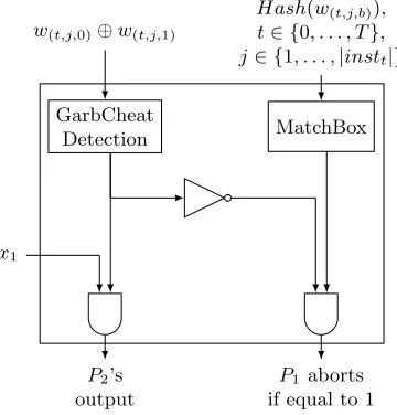
To revealP1’s input, we compute the AND of output of circuit of Figure6 with each bit ofP1’s input
as depicted in Figure7. This concludes the description of the first component for cheating recovery.
• In the second component, we check the authenticity of the memory instructions P2 provided in all
timesteps. In particular, he provides the hash of concatenation of all output authentication labels he obtained during the evaluation corresponding toinstin all timesteps (P2 uses dummy labels if he does
not have valid ones due toP1’s cheating), whileP1does the same based on the plaintext instructions
he received fromP2and the labels which he knows. The circuit then outputs 1 if the two hash values
match. The circuit structure is therefore identical to that of Figure 5, but the inputs are the hash values. An output of 0 would mean thatP2 does not have a valid proof of authenticity.
As shown in the final circuit of Figure 7 then, if P1 was not already caught cheating in the previous
step, and P2’s proof of authenticity fails, the circuit outputs a 1 to signal an abort to P1. This is a
crucial condition, i.e., it is important to ensure P1 did not cheat (the output of circuit of Figure 6)
before accusing P2 of cheating, since in case of cheating by P1 say in timestept, P2 may be able to
prove authenticity of the instructions for timesteptor later.
Efficiency: Following the techniques of [Lin13], all the gates of Figures 5, and 6 can be garbled using non-cryptographic operations (XORs) and only the circuit of Figure7 has non-XOR gates. More precisely it requires|x1|ANDs and a NOT gate.
Of course, the final circuit will be evaluate using a basic maliciously secure 2PC. Thus, we need to add a factor of 3sto the above numbers which results in garbling a total of 3s(|x1|+ 1) non-XOR gates which is
at most 12s(|x1|+ 1) symmetric operations.
The input consistency checks are also done for P1’s inputx1 andP2’s input which is a proof of cheating
of length|∆|and a proof of authenticity which is the output of a hash function (both are in the order of the computational security parameter). We stress that the gain is significant since both the malicious 2PC and the input consistency cheks are only done once at the end.
5
Optimizations
∆t[0]
(w(t,j,0)⊕w(t,j,1))[0]
∆t[1]
(w(t,j,0)⊕w(t,j,1))[1]
∆t[m]
(w(t,j,0)⊕w(t,j,1))[m]
outt
MatchBoxt
Figure 5: Cheating recovery component 1: MatchBox. Where ∆t[i] denotes theith bit of ∆tandm=|∆t|.
MatchBox0
MatchBox1
MatchBoxT
w(t,j,0)⊕w(t,j,1) garbler
cheated GarbCheatDetection
Figure 6: Cheating Recovery component 1: Garbler Cheating Detection.
5.1
Hide only the input-dependent behavior
Systems like SCVM [LHS+14] use static program analysis to “factor out” as much input-independent program
flow as possible from a RAM computation, leaving significantly less residual computation that requires protection from the 2PC mechanisms.
The backend protocol currently implemented by SCVM achieves security only against semi-honest ad-versaries. However, our protocols are also compatible with their RAM-level optimizations, which we discuss in more detail:
Special-purpose circuits. For notational simplicity, we have described our RAM programs via asingle
circuit Π that evaluates each timestep. Then Π must contain subcircuits for every low-level instruction (addition, multiplication, etc) that may ever be needed by this RAM program.
Instruction-trace obliviousness means that the choice of low-level instruction (e.g., addition, mul-tiplication) performed at each time t does not depend on private input. The SCVM system can compile a RAM program into an instruction-trace-oblivious one (though one does not need full instruction-trace obliviousness to achieve an efficiency gain in 2PC protocols). For RAM programs with this property, we need only evaluate an (presumably much smaller) instruction-specific circuit Πtat each timestept.
It is quite straight-forward to evaluate different circuits at different timesteps in our cut-and-choose protocol of Section4. For the batching protocol of Section3, enough instruction-specific circuits must be generated in the pre-processing phase to ensure a majority of correct circuits in each bucket. However, we point out that buckets at different timesteps could certainly be different sizes! One particularly interesting use-case would involve a very aggressive pre-processing of the circuits involved in the ORAM construction (i.e., the logic translating logical memory accesses to physical accesses), since these will dominate the com-putation and do not depend on the functionality being computed.5 The bucket size / replication factor for these timesteps could be very low (say, 5), while the less-aggressively pre-processed instructions could have
w(t,j,0)⊕w(t,j,1)
Hash(w(t,j,b)),
t∈ {0, . . . , T}, j∈ {1, . . . ,|instt|}
GarbCheat
Detection MatchBox
x1
P2’s
output
P1 aborts
if equal to 1
Figure 7: Final Circuit
larger buckets. In this case, the plain-RAM internal state could be kept separate from the ORAM-specific internal state, and only fed into the appropriate circuits.
Along similar lines, we have for simplicity described RAM programs that require a random input tape at each timestep. This randomness leads to oblivious transfers within the protocol. However, if it is known to both parties that a particular instruction does not require randomness, then these OTs are not needed. For example, deterministic algorithms require randomness only for the ORAM mechanism. Concretely, tree-based ORAM constructions [SCSL11,SvDS+13, CP13] require only a small amount of randomness and at
input-indepenent steps.
Memory-trace obliviousness. Due to their general-purpose nature, ORAM constructions protect all
memory accesses, even those that may already be input-independent (for example, sequantial iteration over an array). One key feature of SCVM is detecting which memory accesses are already input-independent and not applying ORAM to them. Of course, such optimizations to a RAM program would yield benefit to our protocols as well.
5.2
Reusing memory
We have described our protocols in terms of a single RAM computation on an initially empty memory. How-ever, one of the “killer applications” of RAM computations is that, after an initial quasi-linear-time ORAM initialization of memory, future computations can use time sublinear in the total size of data (something that is impossible with circuits). This requires an ORAM-initialized memory to be reused repeatedly, as in [GKK+12].
Our protocols are compatible with reusing garbled memory. In particular, this can be viewed as a single RAM computation computing a reactive functionality (one that takes inputs and gives outputs repeatedly).
5.3
Other Protocol Optimizations
Storage requirements for RAM memory. In our cut-and-choose protocol, P1 chooses random wire
labels to encode bits of memory, and then has to remember these wire labels when garbling later circuits that read from those locations. As an optimization, P1 could instead choose wire labels viaFk(t, j, i, b), where F is a suitable PRF, t is the timestep in which the data was written, j is the index of a thread, i is the bit-offset within the data block, andbis the truth value. Since memorylocationsare computed at run-time, P1cannot include the memory location in the computation of these wire labels. Hence, P1 will still need to
Adaptive garbling. In the batching protocol, P1 must commit to the garbled circuits and reveal them
only afterP2obtains the garbled inputs. This is due to a subtle issue of (non)adaptivity in standard security
definitions of garbled circuits; see [BHR12a] for a detailed discussion. These commitments could be avoided by using an adaptively-secure garbling scheme.
Online/offline tradeoff. For simplicity we described our online/offline protocol in which P1 generates
many garbled circuits and P2 opens exactly half of them. Lindell and Riva [LR14] also follow a similar
approach of generating many circuits in an offline phase and assigning the remainder to random buckets; they also point out that changing the fraction of opened circuits results in different tradeoffs between the amount of circuits used in the online and offline phases. For example, checking 20% of circuits results in fewer circuits overall (i.e., fewer generated in the offline phase) but larger buckets (in our setting, more garbled circuits per timestep in the online phase).
References
[ALSZ13] Gilad Asharov, Yehuda Lindell, Thomas Schneider, and Michael Zohner. More efficient oblivious transfer and extensions for faster secure computation. In Sadeghi et al. [SGY13], pages 535–548.
[Bea97] Donald Beaver. Commodity-based cryptography (extended abstract). In 29th Annual ACM Symposium on Theory of Computing, pages 446–455. ACM Press, May 1997.
[BHR12a] Mihir Bellare, Viet Tung Hoang, and Phillip Rogaway. Adaptively secure garbling with applications to one-time programs and secure outsourcing. In Xiaoyun Wang and Kazue Sako, editors, Advances in Cryptology – ASIACRYPT 2012, volume 7658 of Lecture Notes in Computer Science, pages 134–153. Springer, December 2012.
[BHR12b] Mihir Bellare, Viet Tung Hoang, and Phillip Rogaway. Foundations of garbled circuits. In Yu et al. [YDG12], pages 784–796.
[CG13] Ran Canetti and Juan A. Garay, editors.Advances in Cryptology – CRYPTO 2013, Part II, volume 8043 ofLecture Notes in Computer Science. Springer, August 2013.
[CP13] Kai-Min Chung and Rafael Pass. A simple ORAM. Cryptology ePrint Archive, Report 2013/243, 2013.
http://eprint.iacr.org/2013/243.
[DPSZ12] Ivan Damg˚ard, Valerio Pastro, Nigel P. Smart, and Sarah Zakarias. Multiparty computation from some-what homomorphic encryption. In Safavi-Naini and Canetti [SNC12], pages 643–662.
[FJN+13] Tore Kasper Frederiksen, Thomas Pelle Jakobsen, Jesper Buus Nielsen, Peter Sebastian Nordholt, and Claudio Orlandi. MiniLEGO: Efficient secure two-party computation from general assumptions. In Johansson and Nguyen [JN13], pages 537–556.
[GHL+14] Craig Gentry, Shai Halevi, Steve Lu, Rafail Ostrovsky, Mariana Raykova, and Daniel Wichs. Garbled RAM revisited. InEUROCRYPT, 2014.
[GKK+12] S. Dov Gordon, Jonathan Katz, Vladimir Kolesnikov, Fernando Krell, Tal Malkin, Mariana Raykova, and Yevgeniy Vahlis. Secure two-party computation in sublinear (amortized) time. In Yu et al. [YDG12], pages 513–524.
[GMW87] Oded Goldreich, Silvio Micali, and Avi Wigderson. How to play any mental game or A completeness theorem for protocols with honest majority. In Alfred Aho, editor, 19th Annual ACM Symposium on Theory of Computing, pages 218–229. ACM Press, May 1987.
[GO96] Oded Goldreich and Rafail Ostrovsky. Software protection and simulation on oblivious RAMs. J. ACM, 43(3):431–473, 1996.
[HKE13] Yan Huang, Jonathan Katz, and David Evans. Efficient secure two-party computation using symmetric cut-and-choose. In Canetti and Garay [CG13], pages 18–35.
[HKK+14] Yan Huang, Jonathan Katz, Vladimir Kolesnikov, Ranjit Kumaresan, and Alex J. Malozemoff. Amortizing garbled circuits. InAdvances in Cryptology – CRYPTO 2014., 2014.


![Figure 5: Cheating recovery component 1: MatchBox. Where ∆t[i] denotes the ith bit of ∆t and m = |∆t|.](https://thumb-us.123doks.com/thumbv2/123dok_us/7906971.1312880/17.612.172.445.240.362/figure-cheating-recovery-component-matchbox-denotes-ith-bit.webp)