An Optimized Design Methodology
&Synthesis for Stability of
-Pole
Current-Mode Active-R Filter
Adnan Abdullah Qasem
1, G. N. Shinde
2School of Physics, S.R.T.M. University, Nanded, Maharashtra, India1.
Principal, Indira Gandhi (SR) College, CIDCO, Nanded, Maharashtra, India2.
ABSTRACT: The study proposes an optimized design methodology & synthesis for stability of -pole current-mode
active-R filter for =20 KHz and Q-factor =1. This paper illustrates a new configuration to realize the stability of
-pole current-mode active-R filter. The proposed circuit implements three transfer functions lowpass, bandpass, and highpass concurrently in single circuit with work at different nodes with gratified results. It observed that, all poles of transfer functions have negative real parts, and they are lying within the left-half of the s-plane. The return ratio of Nyquist diagram does not enclose the critical point (-1, 0) for all transfer functions. The gain ( ) and phase ( ) margins are both positive. Thus the closed-loop for all transfer functions of -pole current-mode active-R filter at
different nodes are asymptotically stable. This filter is stable for 1Hz ≤ ≥1449 KHz for Q-factor = 1. The output and
input gains are identical at gain cross over frequency. The benefits of this filter are the reducing in weight and size, increasing of circuit quality with wide range for frequency, and it is easier and more economical for producing.
KEYWORDS:Stability, -pole current-mode, active-R filter, Bode diagram, Pole/Zero Map, Step response,
Nyquist diagram.
I. INTRODUCTION
In this paper, -pole current-mode active-R filter one input and three outputs multifunction has been presented. This
paper will discuss the stability of -pole current-mode active-R filter. This active filter is designed with operational
amplifier and resistors only. Analog filters are important building blocks and widely used for continuous-time signal processing [1]. In recent years, the current mode analogue signal processing circuit techniques have received wide attention due to the high accuracy, the wide signal bandwidth and the simplicity of implementing signal operations [2, 3]. In filter circuit designs, current-mode filters are becoming popular since they have many advantages compared with their voltage-mode counter parts, the current-mode filters have large dynamic range, higher bandwidth, greater linearity, simple circuitry, and low power consumption etc. [4-6].Current-mode filter theoretically should exhibit high output impedance (Ideally infinite) and low input impedance (Ideally Zero) [4-10].In this filter, we use at least ten
passive components such as resistor and three active components such as operation amplifier to realize -pole
current-mode active-R filter.
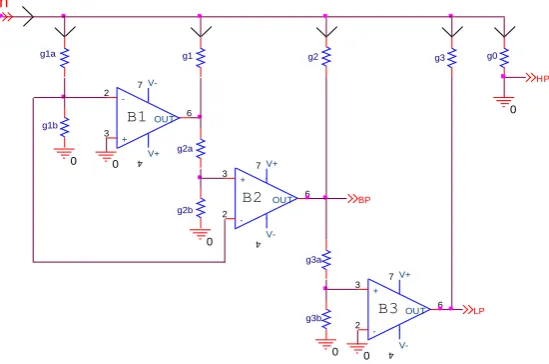
II. PROPOSED CIRCUIT CONFIGURATION
The proposed circuit configuration for an optimized design methodology & synthesis for stability of -pole
current-mode active-R filter is as shown in Fig 1. The circuit consists of three Operational Amplifiers (OAs) (LF356N) with
wide identical gain bandwidth product (GBP=6.392 MHz) and ten Resistors. Resistors (formed by and ) assist
voltage-divider arrangement. The input sinusoidal low current is applied to the inverting terminal of the first op-amp
through first voltage-divider (formed by and ). The non-inverting terminal is grounded. The output of the first
op-amp is connected to non-inverting input of second op-amp through second voltage-divider (formed by and ).
The feed forward input signal is given to the inverting terminal of the second op-amp. The output of the second op-amp
is connected to non-inverting input of third op-amp through third voltage-divider (formed by and ). The
executes three transfer functions (lowpass, bandpass and highpass) at three different nodes. The lowpass, bandpass and highpass transfer functions are as shown in Fig 1.
g1a
+ 3
-2
V+ 7
V-4
OUT 6
+ 3
-2
V+ 7
V-4
OUT 6 g1b
+ 3
-2
V+ 7
V-4
OUT 6
0
g1 g2 g3 g0
g2a
g2b
g3a
g3b
0
0
0 0
0
B1
B2
B3 Iin
HP
BP
LP
Fig 1: An Optimized Design Methodology & Synthesis for Stability of -pole Current-Mode Active-R Filter.
III. CIRCUIT ANALYSIS AND DESIGN EQUATIONS
Op-amp (LF356N) is an internally compensated op-amp, which is represented by “a single-pole model”,
Where,
= open loop D.C. gain, = open loop -3dB bandwidth, β = = gain bandwidth product of op-amplifier.
Here .
This shows that the op-amplifier is an “integrator”. Thus, the transfer functions at three different nodes are given below.
The current-mode transfer function for lowpass filter:
The current-mode transfer function for bandpass filter:
The current-mode transfer function for highpass filter:
, and
The circuit was designed using coefficient matching technique viz by comparing these transfer functions with General
-order transfer function [8]. The general -order transfer function is given by
(6)
By comparing (3), (4), and (5) with (6), we get the design equations as
So that values of, , , and can be calculated using these equations for the values of =20 KHz, Q =1 and
= = =0.5 mS (table1).
Table 1: Resistance values for the values of & Q =1.
(kHz) (kΩ ) (kΩ ) (Ω ) (Ω )
20 987.48 12.44 78.1 0.25
IV. SENSITIVITY
Passive and active sensitivities are smaller than unity. These values ensure the stability of the circuit.
V. EXPERIMENTAL SET UP
The circuit consists of three operational amplifiers (OAs) (LF356N) with wide identical gain bandwidth product
(GBP=6.392 MHz) and ten Resistors. Resistors (formed by and ) assist voltage-divider arrangement. The circuit
performance is studied for values of =20 KHz with the circuit Q-factor =1. The general operating range of this filter
is 10 Hz to 10 MHz. The value of β ( = = ) is ( rad/sec) and k ( = = ) is 0.5 mS. The
voltage-dividers have high input impedances and low output impedances. The input sinusoidal low current is applied to
the inverting terminal of the first op-amp through first voltage-divider (formed by and ).
VI. RESULT AND DISCUSSION
The following observations are noticed for the stability of lowpass, bandpass and highpass at corresponding nodes.
A.THE STABILITY OF LOWPASS RESPONSE:
(a) Bode diagram for lowpass response:
Fig 2 shown bode diagram for the lowpass response of -pole current-mode active-R filter. The data obtained from
the analysis bode diagram for the lowpass response curve is as shown in table 2.The phase cross over frequency is
at 28.3 KHz when the phase is at -180°, then gain is -9.54 dB at 28.3 KHz, so that the gain is less than zero dB, then the
feedback system of -pole current-mode active-R filter is stable. The gain cross over frequency is at 0.173 KHz,
when the gain is at 0 dB, then phase is -1° at 0.173 KHz. The gain margin is 9.54 dB at 28.3 KHz, while the phase
margin is 179° at 0.173 KHz, then the gain ( ) and phase ( ) margins are both positive. Thus the lowpass response
of -pole current-mode active-R filter is asymptotically stable. The output and input gains are identical at 0.173 KHz.
The phase (degrees) response of -pole current-mode active-R filter is shown in Fig 2. It varies from 0° at low frequencies to −270° at high frequencies.
-100 -80 -60 -40 -20 0
M
a
g
n
it
u
d
e
(
d
B
)
10-1 100 101 102 103
-270 -225 -180 -135 -90 -45 0
P
h
a
se
(
d
e
g
)
Bode Diagram
Gm = 9.54 dB (at 28.3 kHz) , Pm = 179 deg (at 0.173 kHz)
Frequency (kHz)
Table 2: Graph analysis of Fig 2.
For Gain Margin For Phase Margin
Phase Gain Gain
Margin
Gain Phase Phase
Margin Ø
(deg) (KHz)
dB
(KHz) (dB) (KHz)
dB
(KHz) Ø
(deg) (KHz) (deg) (KHz)
-180 28.3 -9.54 28.3 9.54 28.3 0 0.173 -1 0.173 179 0.173
:- Gain Cross Over Frequency :- Gain Margin
:- Phase Cross Over Frequency :- Phase Margin
(b) Pole/Zero Map for lowpass response:
Fig 3 shown the pole/zero map for lowpass response for values of =20 KHz and Q =1. The Zeros and Poles of lowpass response are given as Z =0, 0 and 0 where these three Zeros are at infinity, and Poles at1.26×10^5, and
-6.28×10^4 1.09×10^5. It observed that, all poles have negative real parts, and they are lying within the left-half of the
s-plane. Thus the lowpass response is asymptotically stable. The locations of the Poles of -pole current-mode
active-R filter are shown in Fig 3.The zero is marked by a circle (o) and the pole is marked by a cross (×).
Pole-Zero Map for Low-pass response
Real Axis (seconds-1)
Im a g in a ry A xi s (se co n d s -1)
-14 -12 -10 -8 -6 -4 -2 0
x 104
-1.5 -1 -0.5 0 0.5 1
1.5x 10
5
System: TLP Pole : -6.28e+04 + 1.09e+05i Damping: 0.5 Overshoot (%): 16.3 Frequency (kHz): 20 System: TLP
Pole : -1.26e+05 Damping: 1 Overshoot (%): 0 Frequency (kHz): 20
System: TLP Pole : -6.28e+04 - 1.09e+05i Damping: 0.5 Overshoot (%): 16.3 Frequency (kHz): 20
0.08 0.16 0.26 0.36 0.48 0.62 0.78 0.94 0.08 0.16 0.26 0.36 0.48 0.62 0.78 0.94 5 10 15 20 5 10 15 20
Fig 3: The pole/zero map for lowpass response for values of =20 KHz and Q=1.
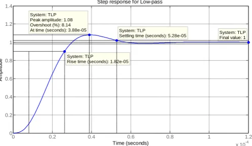
(c) Step response for lowpass response:
Fig 4 shown the step response for lowpass response of -pole current-mode active-R filter. It is observed that, the poles are complex. Thus the system of lowpass response is under-damped with an overshoot, it is 0.08 dB and that is as shown in Fig 4. The characteristics response obtained from the analysis step response of lowpass response curve is as shown in table 3.
Step response for Low-pass
Time (seconds) A m p lit u d e
0 0.2 0.4 0.6 0.8 1 1.2
x 10-4 0 0.2 0.4 0.6 0.8 1 1.2 1.4 System: TLP
Rise time (seconds): 1.82e-05 System: TLP
Peak amplitude: 1.08 Overshoot (%): 8.14
At time (seconds): 3.88e-05 System: TLP
Settling time (seconds): 5.28e-05 System: TLPFinal value: 1
Table 3: Graph analysis of Fig 4.
Peak amplitude Rise time
(sec)
Setting time (sec)
Final value at (dB)
Overshoot
dB
Time (sec)
dB %
1.08 3.88×10^-5 1.82×10^-5 5.28×10^-5 1 0.08 8.14
(d) Nyquist diagram for lowpass response:
The Nyquist diagram for lowpass response of -pole current-mode active-R filter is as shown in Fig 5. It observed
that, the return ratio of Nyquist diagram for lowpass response does not enclose the critical point (-1, 0). Thus the
closed-loop for lowpass response of -pole current-mode active-R filter is asymptotically stable. The Gain margin is
9.54 dB at 28.3 KHz, and the phase margin is 179° at 0.173 KHz.
Nyquist Diagram for Low-pass response
Real Axis
Im
a
g
in
a
ry
A
xi
s
-1 -0.5 0 0.5 1 1.5
-1 -0.8 -0.6 -0.4 -0.2 0 0.2 0.4 0.6 0.8 1
0 dB
-20 dB -10 dB
-6 dB
-4 dB -2 dB
20 dB 10 dB 6 dB 4 dB2 dB
System: TLP Gain Margin (dB): 9.54 At frequency (kHz): 28.3 Closed loop stable? Yes
System: TLP Phase Margin (deg): 179 Delay Margin (sec): 0.00287 At frequency (kHz): 0.173 Closed loop stable? Yes
Fig 5: The Nyquist diagram for lowpass response for values of =20 KHz &Q = 1.
B.THE STABILITY OF BANDPASS RESPONSES:
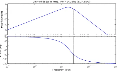
(a) Bode diagram for band pass response:
Fig 6 shown bode diagram for bandpass response of -pole current-mode active-R filter. The data obtained from the
analysis bode diagram for the bandpass response curve is as shown in table 4.The phase cross over frequency is at
Infinity KHz when the phase is at -180°, then gain is Infinity dB at Infinity KHz. The gain cross over frequency is
at 27.2 KHz, when the gain is at 0 dB, then phase is -85.8° at 27.2 KHz. The gain margin is Infinity dB at Infinity KHz, while the phase margin is 94.2° at 27.2 KHz, then gain ( ) and phase ( ) margins are both positive. Thus the bandpass response of -pole current-mode active-R filter is asymptotically stable. The output and input gains are
identical at 27.2 KHz. The phase (degrees) response of -pole current-mode active-R filter is shown in Fig 6. It varies
from 90° at low frequencies to -180° at high frequencies.
-50 -40 -30 -20 -10 0 10
M
a
g
n
it
u
d
e
(
d
B
)
10-1 100 101 102 103
-180 -135 -90 -45 0 45 90
P
h
a
se
(
d
e
g
)
Bode Diagram
Gm = Inf dB (at Inf kHz) , Pm = 94.2 deg (at 27.2 kHz)
Frequency (kHz)
Table 4: Graph analysis of Fig 6.
For Gain Margin For Phase Margin
Phase Gain Gain
Margin
Gain Phase Phase
Margin Ø
(deg) (KHz)
dB
(KHz) (dB) (KHz)
dB
(KHz) Ø
(deg) (KHz) (deg) (KHz)
-180 Infinity Infinity Infinity Infinity Infinity 0 27.2 -85.8 27.2 94.2 27.2
:- Gain Cross Over Frequency :- Gain Margin
:- Phase Cross Over Frequency :- Phase Margin
(b) Pole/Zero Map for bandpass response:
Fig 7 shown the pole/zero map for bandpass response for values of =20 KHz and Q-factor =1. The Zeros and Poles
of bandpass response are given as Z =0, 0 and 0, where two Zeros are at infinity while one Zero is at the origin, and Poles at -1.26×10^5, and -6.28×10^4 1.09×10^5. It observed that, all poles have negative real parts, and they are lying within the left-half of the s-plane. Thus the bandpass response is asymptotically stable. The locations of the Poles
of -pole current-mode active-R filter are shown in Fig 7.
Pole-Zero Map for Band-pass response
Real Axis (seconds-1)
Im a g in a ry A xi s (se co n d s -1)
-14 -12 -10 -8 -6 -4 -2 0
x 104
-1.5 -1 -0.5 0 0.5 1
1.5x 10
5 0.26 0.36 0.48 0.62 0.78 0.94 0.08 0.16 0.26 0.36 0.48 0.62 0.78 0.94 5 10 15 20 5 10 15 20 System: TBP Pole : -6.28e+04 + 1.09e+05i Damping: 0.5 Overshoot (%): 16.3 Frequency (kHz): 20 System: TBP
Pole : -1.26e+05 Damping: 1 Overshoot (%): 0 Frequency (kHz): 20
System: TBP Zero : 0 Damping: -1 Overshoot (%): 0 Frequency (kHz): 0 System: TBP
Pole : -6.28e+04 - 1.09e+05i Damping: 0.5 Overshoot (%): 16.3 Frequency (kHz): 20
0.08 0.16
Fig 7: The pole/zero map for bandpass response for values of =20 KHz &Q = 1.
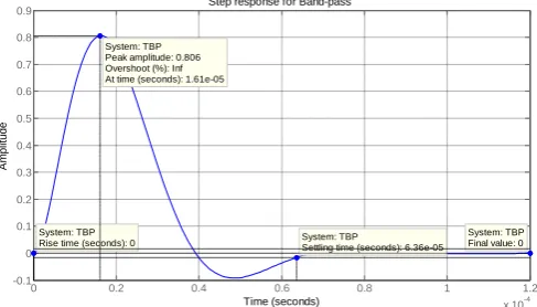
(c) Step response for bandpass response:
Fig 8 shown the step response for bandpass response of -pole current-mode active-R filter. It is observed that, the
poles are complex. Thus the system of bandpass response is under-damped with an overshoot, it is 0.806 dB and that is as shown in Fig 8. The characteristics response obtained from the analysis step response of bandpass response curve is as shown in table 5.
Step response for Band-pass
Time (seconds) A m p lit u d e
0 0.2 0.4 0.6 0.8 1 1.2
x 10-4 -0.1 0 0.1 0.2 0.3 0.4 0.5 0.6 0.7 0.8 0.9 System: TBP Rise time (seconds): 0
System: TBP Peak amplitude: 0.806 Overshoot (%): Inf At time (seconds): 1.61e-05
System: TBP
Settling time (seconds): 6.36e-05
System: TBP Final value: 0
Table 5: Graph analysis of Fig 8.
Peak amplitude Rise time
(sec)
Setting time
(sec) Final value at
dB
Overshoot
dB
Time (sec)
dB %
0.806 1.61×10^-5 0 6.36×10^-5 0 0.806 Infinity
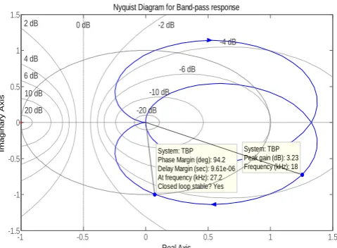
(d) Nyquist diagram for bandpass response:
The Nyquist diagram for bandpass response of -pole current-mode active-R filter is as shown in Fig 9. It observed
that, the return ratio of Nyquist diagram for bandpass response does not enclose the critical point (-1, 0). Thus the
closed-loop for bandpass response of -pole current-mode active-R filter is asymptotically stable. The Gain margin is
Infinity dB at Infinity KHz, and the phase margin is 94.2° at 27.2 KHz.
Nyquist Diagram for Band-pass response
Real Axis
Im
a
g
in
a
ry
A
xi
s
-1 -0.5 0 0.5 1 1.5
-1.5 -1 -0.5 0 0.5 1 1.5
0 dB
-20 dB -10 dB
-6 dB -4 dB -2 dB
20 dB 10 dB 6 dB 4 dB 2 dB
System: TBP Phase Margin (deg): 94.2 Delay Margin (sec): 9.61e-06 At frequency (kHz): 27.2 Closed loop stable? Yes
System: TBP Peak gain (dB): 3.23 Frequency (kHz): 18
Fig 9: The Nyquist diagram for bandpass response for values of =20 KHz &Q = 1.
C. THE STABILITY OF HIGHPASS RESPONSE:
(a) Bode diagram for highpass response:
Fig 10 shown bode diagram for the highpass response of -pole current-mode active-R filter. The data obtained from
the analysis bode diagram for the highpass response curve is as shown in table 6.The phase cross over frequency is
-100 -50 0 M a g n it u d e ( d B )
10-1 100 101 102 103
0 45 90 135 180 225 270 P h a se ( d e g ) Bode Diagram Gm = 9.65 dB (at 14.1 kHz) , Pm = Inf
Frequency (kHz)
Fig 10: Bode diagram for highpass response for values of =20 KHz &Q = 1. Table 6: Graph analysis of Fig 10.
For Gain Margin For Phase Margin
Phase Gain Gain
Margin
Gain Phase Phase
Margin Ø
(deg) (KHz)
dB
(KHz) (dB) (KHz)
dB
(KHz)
Ø
(deg) (KHz) (deg) (KHz)
-180 14.1 -9.65 14.1 9.65 14.1 0 Infinity Infinity Infinity Infinity Infinity
:- Gain Cross Over Frequency :- Gain Margin
:- Phase Cross Over Frequency :- Phase Margin
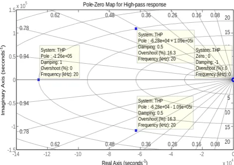
(b) Pole/Zero Map for highpass response:
Fig 11 shown the pole/zero map for high pass response for values of =20 KHz and Q-factor = 1. The Zeros and Poles of highpass response are given as Z =0, 0 and 0, where three Zeros are at the origin, and Poles at 1.26×10^5, and
-6.28×10^4 1.09×10^5. It observed that, all poles have negative real parts, and they are lying within the left-half of the
s-plane. Thus the highpass response is asymptotically stable. The locations of the Poles of -pole current-mode active-R filter are shown in Fig 11.
Pole-Zero Map for High-pass response
Real Axis (seconds-1)
Im a g in a ry A xi s (se co n d s -1)
-14 -12 -10 -8 -6 -4 -2 0
x 104 -1.5 -1 -0.5 0 0.5 1 1.5x 10
5 0.26 0.36 0.48 0.62 0.78 0.94 0.08 0.16 0.26 0.36 0.48 0.62 0.78 0.94 5 10 15 20 5 10 15 20 System: THP Pole : -6.28e+04 + 1.09e+05i Damping: 0.5 Overshoot (%): 16.3 Frequency (kHz): 20
System: THP Pole : -6.28e+04 - 1.09e+05i Damping: 0.5 Overshoot (%): 16.3 Frequency (kHz): 20 System: THP
Pole : -1.26e+05 Damping: 1 Overshoot (%): 0 Frequency (kHz): 20
System: THP Zero : 0 Damping: -1 Overshoot (%): 0 Frequency (kHz): 0
0.08 0.16
(c) Step response for highpass response:
Fig 12 shown the step response for highpass response of -pole current-mode active-R filter.It is observed that, the
poles are complex. Thus the system of highpass response is under-damped with an overshoot, it is 0.937 dB and that is as shown in Fig 12. The characteristics response obtained from the analysis step response of highpass response curve is as shown in table 7.
Step response for High-pass
Time (seconds)
A
m
p
li
tu
d
e
0 0.2 0.4 0.6 0.8 1 1.2
x 10-4
-0.4 -0.2 0 0.2 0.4 0.6 0.8 1
System: THP Peak amplitude: 0.987 Overshoot (%): Inf At time (seconds): 0
System: THP
Rise time (seconds): 4.56e-06 System: THP
Settling time (seconds): 5.33e-05
System: THP Final value: 0
Fig 12: The step response for highpass response for values of =20 KHz & Q = 1.
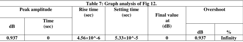
Table 7: Graph analysis of Fig 12.
Peak amplitude Rise time
(sec)
Setting time
(sec) Final value
at (dB)
Overshoot
dB
Time (sec)
dB %
0.937 0 4.56×10^-6 5.33×10^-5 0 0.937 Infinity
(d) Nyquist diagram for highpass response:
The Nyquist diagram for highpass response of -pole current-mode active-R filter is as shown in Fig 13. It observed
that, the return ratio of Nyquist diagram for highpass response does not enclose the critical point (-1, 0). Thus the
closed-loop for highpass response of -pole current-mode active-R filter is asymptotically stable. The Gain margin is
9.55 dB at 14.1 KHz, and the phase margin is Infinity.
Nyquist Diagram for High-pass response
Real Axis
Im
a
g
in
a
ry
A
xi
s
-1 -0.8 -0.6 -0.4 -0.2 0 0.2 0.4 0.6 0.8 1
-1 -0.8 -0.6 -0.4 -0.2 0 0.2 0.4 0.6 0.8 1
0 dB
-20 dB -10 dB
-6 dB
-4 dB -2 dB
20 dB 10 dB 6 dB 4 dB 2 dB
System: THP Gain Margin (dB): 9.65 At frequency (kHz): 14.1 Closed loop stable? Yes
System: THP Peak gain (dB): -0.109 Frequency (kHz): 1e+09
VII. CONCLUSIONS
A realization of stability of -pole current-mode active-R filter for values of =20 KHz and Q-factor=1 has been proposed. The proposed circuit implements three filter functions lowpass, bandpass, and highpass concurrently in single circuit. The three filter functions lowpass, bandpass and highpass work at different nodes with gratified results. The gain ( ) and phase ( ) margins are both positive for all the transfer functions. It observed that, all poles of transfer functions have negative real parts, and they are lying within the left-half of the s-plane. The return ratio of Nyquist diagram does not enclose the critical point (-1, 0) for all transfer functions. The gain ( ) and phase ( ) margins are both positive. Thus the closed-loop for all transfer functions of -pole current-mode active-R filter at different nodes are asymptotically stable. This filter is stable for 1Hz ≤ ≥1449 KHz, for Q-factor =1. The output and input gains are identical at gain cross over frequency.
REFERENCES
[1] F.Kacar&H.Kuntman” new current-mode filter using single FDCCIT with grounded resistors and capacitors” OJEEE, vol. (2)-No (4).
[2] T.Tsutani, T.Higashimura,Y.Sumi and Y.Fukui”electronically tunable current mode active only biquadratic filter” International journal of electronics , vol.87,No.3,pp.307-314, 2000.
[3] G.N.Shinde and D.D.Mulajkar “third-order current mode universal filter using only op.amp and OTAs”scientific research, 1, 65-70, 2010. [4] G.N.Shinde and D.D.Mulajkar “frequency response of electronically tunable current mode third order high pass filter with central frequency
f0=10 KHz with variable circuit merit factor Q” scholar’s research library, 2(3):248-252, 2010.
[5] Toumazou C, Lidjey FJ, Haigh D.Analog IC design: The current-mode approach. Exeter, UK: peter peregrinus, 1990.
[6] Ugurn Cam “anovel current-mode second-order notch filter configuration employing single CDBA and reduced number of passive components” ELSEVIER, 147-151, 2004.
[7] G.W.Roberts&A.S.Sedra, “All current-mode frequency selective circuits”, electronics letters25, 759-761, 1989.
[8] A.A.Qasem&G.N.Shinde “Electronically Tunable Third-Order Switched-Capacitor Filter with Feedforward Signal to Minimize Overshoot”Global Journal of Researches in Engineering: F Electrical and Electronics Engineering Vol 14 Issue 7 Version 1.0 .2014.
[9] D.Biolek, V.Biolkova, Z.kolka&J.Bajer “single-input multi-output resistorless current-mode biquad”.IEEE, 225-228, 2009.