N. Esser
Institut fu¨r Festko¨rperphysik, Technische Universita¨t Berlin, Hardenbergstrasse 36, 10623 Berlin, Germany
W. G. Schmidt and J. Bernholc
Department of Physics, North Carolina State University, Raleigh, North Carolina 27695-8202
A. M. Frisch,a)P. Vogt, M. Zorn, M. Pristovsek, and W. Richter
Institut fu¨r Festko¨rperphysik, Technische Universita¨t Berlin, Hardenbergstrasse 36, 10623 Berlin, Germany
F. Bechstedt
Institut fu¨r Festko¨rpertheorie und Theoretische Optik, Friedrich-Schiller-Universita¨t, Max-Wien-Platz 1, 07743 Jena, Germany
Th. Hannappel and S. Visbeck
Hahn-Meitner Institut, CD, Glienickerstr. 100, 14109 Berlin, Germany 共Received 20 January 1999; accepted 30 March 1999兲
We have investigated the optical anisotropy of GaP共001兲and InP共001兲surfaces. The samples were prepared by homoepitaxial metalorganic vapor phase epitaxy growth and either directly transferred into ultrahigh vacuum共UHV兲or in situ capped and, after transfer, decapped in UHV by thermal desorption of a P/As capping layer. Symmetry, composition, and surface optical anisotropy were characterized by low-energy electron diffraction, Auger electron spectroscopy, and reflectance anisotropy spectroscopy. We observe (2⫻1)/(2⫻2)-like reconstructions for the very P-rich and (2⫻4) reconstructions for the more cation-rich surfaces. No (4⫻2) reconstruction could be prepared, independent of the preparation method. A comparison of the reflectance anisotropy between GaP共001兲and InP共001兲surfaces shows similar line shapes for the very cation-rich (2⫻4) surfaces. For less cation-rich surfaces, however, we observe distinct differences between the spectra of the two systems. In both cases, different line shapes in the reflection anisotropy spectra occur for the (2⫻4) periodicity, suggesting the existence of different (2⫻4) geometries. The experimental results are discussed on the background of atomic structures, total energies and reflectance anisotropy spectra obtained ab initio from density-functional theory local-density approximation calculations. © 1999 American Vacuum Society.关S0734-211X共99兲03504-0兴
I. INTRODUCTION
Much progress has been made in recent years in under-standing the microscopic structure of the growth planes of III–V compound semiconductors 共for a recent review, see, e.g., Ref. 1兲. Optical anisotropy at the same time has been proven to be an additional and complementary tool to elec-tron spectroscopic methods for investigating the microscopic surface structure of semiconductors.2,3 Previous investiga-tions of GaAs共001兲4,5 and InP共001兲6 surfaces have shown that the atomic structure can be successfully clarified in many cases by comparing total energy and band structure calculations for the optical anisotropy on the one hand with experimental data of the optical anisotropy on the other hand. The atomic surface structures of the (2⫻4)-GaP共001兲 and -InP共001兲surfaces were recently investigated by density functional theory local-density approximation 共DFT-LDA兲 total energy calculations.7,8 As in the case of InP共001兲, the atomic structures of GaP共001兲 were found to be different from the well-investigated GaAs共001兲 surface,9–11 due to a large size difference between cations and anions.
While several recent studies have addressed the atomic structure of InP共001兲,8,12–14 much less is known about
GaP共001兲. Available experimental studies lead to different and partially contradictive conclusions about the symmetry and structure of the GaP共001兲 surface. So far it has been suggested mostly that ion bombardment and annealing as well as decapping of GaP共001兲results in a (4⫻2)/c(8⫻2) reconstructed, Ga-rich surface,15–21in analogy to the corre-sponding Ga-rich GaAs共001兲 surface structure.9 In a more recent investigation by ion scattering,22 however, a (2⫻4) symmetry was reported. Similar ambiguous results for GaP共001兲can be found in literature for gas source molecular beam epitaxy 共MBE兲experiments: In Ref. 23 it is reported that (2⫻4) and (4⫻2) reconstruction pattern correspond to P- and Ga-stabilized surfaces, whereas in Ref. 24, a (2⫻4) reconstruction was observed under Ga as well as under P supply. Additionally, the authors of Ref. 24 found an inter-mediate (4⫻4) reconstruction during layer growth and sug-gested the formation of Ga droplets on a (2⫻4) recon-structed surface for high amounts of Ga supply. Only few data can be found in literature about the optical anisotropy of GaP共001兲. To our knowledge, there exist studies of GaP共001兲 surfaces in MBE, metalorganic vapor phase epi-taxy 共MOVPE兲 and chemical beam epitaxy 共CBE兲.25–28 Apart from Ref. 7 no reflectance anisotropy data for GaP共001兲surfaces in ultrahigh vacuum共UHV兲are available. In the present study, clean and well-ordered 共001兲
faces of MOVPE-grown GaP and InP with different stoichi-ometries are prepared under ultrahigh vacuum conditions. All samples are characterized by low-energy electron diffrac-tion共LEED兲, Auger electron spectroscopy共AES兲, and reflec-tance anisotropy spectroscopy 共RAS兲. Based on total-energy 共TE兲calculations and by comparison of experimental data to calculated optical anisotropies for various atomic structure models it is shown that several (2⫻4) reconstructions exist for GaP共001兲 and InP共001兲. They realize different stoi-chiometries. (4⫻2) structures do not occur in either case.
II. METHOD
The GaP共001兲surfaces were prepared by thermal desorp-tion of a protective arsenic/phosphorus double layer 共cap兲 under UHV conditions. For this purpose, homoepitaxial GaP epilayers were grown by MOVPE on highly n-doped (1018cm⫺3) GaP共001兲substrates and capped in situ utilizing the photodecomposition of phosphine and arsine by an exci-mer laser source.27,29共a兲The thermal desorption of the protec-tive arsenic/phosphorus layer was performed at 690 K in UHV at a base pressure⭐10⫺10hPa. The InP共001兲samples were grown by MOVPE on n-doped (1017cm⫺3) InP共001兲 substrates and transferred under UHV conditions in the ana-lyzing UHV chamber directly after growth, without using the capping technique.29共b兲 Starting with P-rich surface condi-tions in either case, different reconstruccondi-tions were prepared by subsequent annealing in UHV. After cooling to room temperature, the surfaces were investigated by LEED, RAS, and AES.
The calculations were based on DFT-LDA. Optical prop-erties are calculated in independent-particle approximation from the DFT-LDA electronic structure. To determine the optical anisotropy, we follow the formalism developed by Del Sole30and Manghi et al.31Computational details can be found in Refs. 6 and 11.
III. RESULTS AND DISCUSSION
A. Surface symmetry and composition
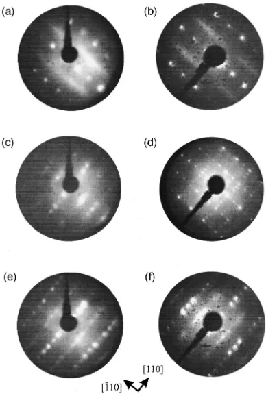
The decapped GaP共001兲 surfaces共after annealing to 690 K兲show a (2⫻1)/(2⫻2)-like LEED pattern关see Fig. 1共a兲兴, with clear (2⫻1) spots plus additional streaks in the关110兴 half order position. A similar LEED pattern关see Fig. 1共b兲兴is observed from InP共001兲 surfaces, directly after transfer into the UHV system. Annealing to 785 and 645 K leads to (2
⫻4) LEED patterns for GaP共001兲 as well as for InP共001兲. The LEED pattern of the (2⫻4) GaP共001兲surface does not allow us to distinguish between a (2⫻4) and a (2
⫻4)/c(2⫻8) reconstruction关Fig. 1共c兲兴due to not fully re-solved fractional order spots in the 关110兴 direction. The LEED pattern of the InP共001兲 surface, on the contrary, shows a (2⫻4) periodicity, or a superposition of 共2⫻1兲/ 共2⫻2兲and 共2⫻4兲 关Fig. 1共d兲兴. Upon further annealing up to 1000 K the quality of the LEED pattern for GaP共001兲 is improved and the former streaks develop into sharp spots indicating a pure (2⫻4) reconstruction, similar to the pat-tern observed for InP共001兲 关Figs. 1共e兲 and 1共f兲兴. Upon
an-nealing to still higher temperatures 关⭓1000 K for GaP共001兲 and ⭓725 K for InP共001兲兴 the symmetry of the LEED pat-terns remains unchanged until the surfaces deteriorate by forming Ga or In droplets, as indicated by a metallic compo-nent in the Ga 3d/In 4d core level photoemission lines 共not shown here兲. AES measurements performed on GaP after decapping and InP after UHV transfer show no detectable carbon or oxygen contaminations. Moreover, the composi-tion of the GaP共001兲surfaces was examined. The P/Ga ratio for the (2⫻1)/(2⫻2)-like GaP共001兲 surface shows P-rich surface conditions, but it cannot be exactly determined be-cause of the P desorption induced by the electron beam. On the (2⫻4) reconstructed GaP共001兲surface at low annealing temperatures共only slightly above 785 K兲, the P/Ga intensity ratio is close to the one of the GaP共110兲cleavage face共 bal-anced stoichiometry兲. Upon annealing to higher temperatures 共1000 K兲 the ratio changes successively by a factor of ap-proximately two towards a Ga-rich surface, suggesting the existence of a more P-rich (2⫻4) at lower and a Ga-rich (2⫻4) reconstruction at higher annealing temperatures.
B. Optical anisotropy: Experimental results
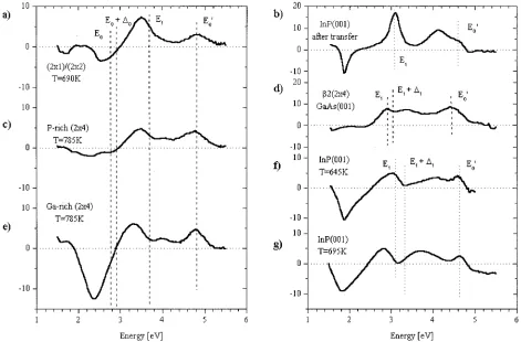
shown in Fig. 2共d兲. Three different spectral line shapes are reproducibly observed on GaP共001兲and InP共001兲, correlated to the surface preparation: a characteristic line shape belongs to the (2⫻1)/(2⫻2)-like structures 关Figs. 2共a兲, 2共b兲兴, and two different line shapes are observed in either case for (2
⫻4) surface structures, one correlated to P-rich conditions at lower annealing temperature 关Figs. 2共c兲, 2共f兲兴 and one to cation-rich conditions at higher annealing temperature关Figs. 2共e兲, 2共g兲兴.
The P-rich GaP共001兲(2⫻4) surface 关Fig. 2共b兲兴shows a spectrum which is qualitatively similar to the one observed for the As dimer terminated 2(2⫻4) GaAs共001兲 surface.3–5It is dominated by pronounced maxima at 3.5 and 4.8 eV, close to the E1and E0
⬘
gap energies of GaP共3.69 and 4.77 eV, respectively32兲and a weak maximum at 4 eV. The RAS spectrum of InP under comparable conditions has a different line shape: In addition to maxima around the bulk critical points E1and E0⬘
共3.16 and 4.68 eV, respectively33兲a
strong minimum at 1.9 eV shows up. We mention that in Ref. 34 a somewhat different spectrum 共nearly no negative anisotropy兲has been assigned to the P-rich phase of InP (2
⫻4). The reason for that difference is not clear at present. The line shapes shown in Figs. 2共f兲 and 2共g兲 are, however, reproducibly observed in our UHV experiments, whereas a line shape comparable to Ref. 34 could not be obtained in spite of repeated attempts. After annealing to higher tem-peratures the RAS spectra for GaP and InP共001兲change and
become similar in line shape. New features in the GaP spec-trum are a strong minimum at 2.4 eV and a maximum at 3.2 eV, significantly below the E1 gap of GaP. On InP the first maximum shifts to somewhat lower energies and an addi-tional maximum appears between E1 and E0
⬘
. On both ma-terials, the maximum at the E0⬘
point remains unaffected.Summarizing the experimental results, there are clear similarities between the very anion-rich (2⫻1)/(2⫻2)-like and the very cation-rich (2⫻4) reconstructed GaP共001兲and InP共001兲surfaces, in particular, if one takes into account the different bulk critical point energies of the two materials. The spectrum of the P-rich (2⫻4) reconstructed GaP共001兲 surface, however, is distinct from the corresponding InP spectrum and resembles the one of GaAs共001兲 2(2⫻4). The evolution of the RAS spectra of GaP共001兲with increas-ing Ga coverage of the surface implies that at least two dis-tinct (2⫻4) structures with different stoichiometry exist on the GaP共001兲surface. This conclusion cannot be drawn for InP共001兲surfaces. Scanning tunneling microscopy images35 imply that the transition structure corresponds to a two-domain surface composed of P-rich共2⫻1兲/共2⫻2兲and In-rich 共2⫻4兲 domains. Also the RAS spectrum 关Fig. 2共f兲兴 can be reproduced by a linear superposition of spectra 2共b兲and 2共g兲.
C. Atomic structure of the surfaces
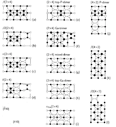
structure of the (2⫻1)/(2⫻2)-reconstructed surfaces is still completely unclear. STM and photoemission data are avail-able for InP共001兲(2⫻4).8,13,29共a兲 TE calculations performed on InP for a large variety of different (2⫻4)- and (4⫻2)-reconstruction models revealed a new type of dimer reconstruction involving mixed In–P surface dimers for In-rich surfaces, consistent with the experimental data.8 Very recently, TE calculations have also been performed for a series of structural models for GaP共001兲.7Figure 3 shows the structural models considered for GaP. One of these models, the ␦(2⫻4) surface structure, which is believed to describe the Sb-induced GaAs (2⫻4) reconstruction,36turned out to be energetically favored for GaP共001兲, but was not consid-ered in earlier studies on InP共001兲. We included that model in the present work.
The investigated models realize different In or Ga cover-ages and can therefore be compared energetically only by taking into account the chemical potentials of the surface constituents.11In Fig. 4 we show the relative formation en-ergies of the considered surface structures vs the cation chemical potential for both InP共001兲and GaP共001兲surfaces. The phase diagrams show following fundamental similari-ties:
共i兲 (2⫻4) structures represent the stable surfaces under cation-rich conditions, in contrast to the GaAs共001兲 case where (4⫻2) structures are known to exist under cation-rich conditions.
共ii兲A new atomic surface structure, consisting of mixed cation–P dimers adsorbed on top of a complete cation layer
关Fig. 3共g兲兴 represents the lowest energy structure over a prominent range of chemical potentials.
共iii兲 For a certain range of preparation conditions, the ␦ geometry关Fig. 3共d兲兴may occur. Given the limited accuracy of our calculations,11 further structures such as␣and top P dimer 关Figs. 3共c兲 and 3共e兲兴 cannot be excluded for the tran-sition between cation- and anion-rich surfaces. Finally, under P-rich conditions P dimers in a 2(2⫻4) geometry 关Fig. 3共b兲兴, as known from As-rich GaAs共001兲surfaces,10,37 rep-resent the lowest energy structure. However, this result must be taken with caution, since for P-rich conditions the experi-mental results indicate the appearance of (2⫻1)/(2⫻2) structures on both GaP as well as InP, which were not con-sidered in the TE calculations.
共iv兲All equilibrium structures are in agreement with elec-tron counting heuristics.38
The similarity between the surface phase diagrams of InP and GaP points towards a common mechanism: The size FIG. 3. Top view of relaxed GaP共001兲(2⫻4) and (4⫻2) surface
recon-struction models. Empty 共filled兲 circles represent Ga 共P兲 atoms. Large
共small兲symbols indicate positions in the first and second共third and fourth兲 atomic layers. (2⫻4) and (4⫻2) reconstructions are ordered by increasing Ga coverage.
FIG. 4. 共a兲 Relative formation energy per (1⫻1) unit cell for GaP共001兲 surface reconstructions vs⌬(Ga)ªbulk(Ga)⫺(Ga). The approximate
thermodynamically allowed range:⫺⌬Hf(GaP)⭐⌬(Ga))⭐0 is indicated
difference between anions and cations hinders the accommo-dation of s p2-hybridized cation dimer atoms that are typical for cation-rich GaAs共001兲surfaces. Instead, the formation of single-dimer structures is favored for cation-rich surfaces.
Besides these similarities, however, there is also an obvi-ous difference: On InP共001兲 the mixed-dimer structure ap-pears to be the only stable geometry under In-rich condi-tions, while on GaP共001兲the top-Ga dimer model关Fig. 3共h兲兴 is lower in energy in the extreme cation-rich limit.
The phase diagrams of GaP and InP in Fig. 4 demonstrate the existence of different stable (2⫻4) surface phases de-pending on the value of the cation chemical potential, i.e., the surface preparation conditions. This finding is in excel-lent agreement with the qualitative evolution of the surface optical anisotropy on GaP共001兲.
Since RAS as an optical technique is applicable in UHV as well as gas phase surroundings, the dependence of InP and GaP surface structures on different environments 共e.g., growth conditions in MOVPE, MBE, CBE, and UHV兲 can be addressed by comparing the RAS spectra taken under dif-ferent conditions. Comparing our spectra with the ones taken in MOVPE and CBE reveal, that for InP as well as for GaP, the same line shapes occur in the different environ-ments.26–28,39 Moreover, an excellent agreement between symmetry observed by RHEED in CBE28,39and LEED in our UHV experiments is found in both InP and GaP cases. There is, however, one exception: A2(2⫻4) seemingly observed in MBE for InP共001兲34is not showing up in our experiments.
D. Optical anisotropy: Calculation
As shown above, the evolution of the surface optical an-isotropy and the calculated equilibrium surface structures is qualitatively consistent. An even more direct comparison be-tween theory and measurement, however, is desirable in or-der to identify specific surface structures. To this end, we compare the computed surface reflectance anisotropy of the energetically favored structures with the experimental RAS spectra.
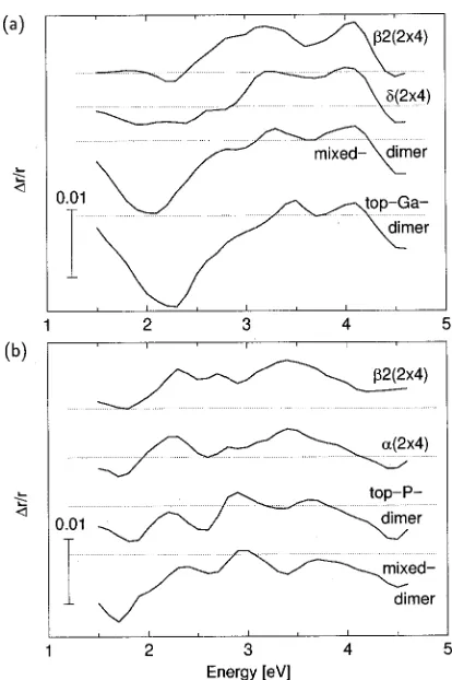
Simulated spectra for GaP共001兲 are shown in the upper panel of Fig. 5.7Earlier we have shown that surface related transitions dominate the low-energy part while bulk-related transitions are more pronounced in the high-energy part of the RAS spectra.7 The top-Ga dimer, mixed dimer, and ␦ structures show a pronounced negative anisotropy in the low-energy region, with minima between 2.0 and 2.3 eV. The strength of that anisotropy is directly correlated to the number of Ga–Ga bonds along the关110兴direction. Its mag-nitude is the highest for the top-Ga-dimer model with eight bonds, slightly reduced and shifted to lower energies for the mixed-dimer geometry with six cation–cation bonds and flattened for the ␦structure with only two such bonds.
The positive anisotropy in the high energy region of the spectra is correlated to the formation of P–P dimers oriented along 关¯ 101 兴: For the 2 geometry with three P–P dimers, we find a relatively strong positive anisotropy between about 2.4 and 4.4 eV. The shape of that anisotropy is roughly pre-served for the␦structure, featuring one P–P dimer, however,
with reduced magnitude and the spectrum is shifted down. An even further reduction in positive anisotropy occurs for the mixed-dimer and top-Ga-dimer structures 共no P–P dimers兲.
According calculations for InP共001兲6 are shown in the lower panel of Fig. 5. Similar systematic trends as for GaP共001兲are observed in the optical anisotropy of InP共001兲: cation-rich surfaces show a characteristic strong minimum at low energies, P-dimer terminated ones a broad positive an-isotropy at higher energies.
In fact, apart from some energy shift due to the neglect of many-body effects in DFT-LDA, the calculated spectra are in rather good agreement with the experimental optical an-isotropy. Together with the calculated phase diagrams they allow a conclusive comparison. The RAS spectra measured for the (2⫻4) structures at higher annealing temperature 共In/Ga-rich phases兲feature a strong negative peak in the low-energy region. Given the low-energy position of this peak and its dependence on the preparation conditions, it can be identified with the calculated negative anisotropy arising from cation– cation surface bond related states. Both the top-Ga-dimer model and the mixed-dimer model thus are plausible candi-dates to explain the Ga-rich surface phase on GaP共001兲, while on InP the mixed-dimer model represents the only pos-sible structure under In-rich conditions.
ture annealed at lower temperature 共more P-rich phase兲 is dominated by a ‘‘camelback’’ overall spectrum shape with maxima between the energies of the E0and E1critical points and at the E0
⬘
bulk peak. No negative anisotropy appears. The only computed spectrum with no 共or very little兲 negative anisotropy belongs to the 2(2⫻4) structure. Maxima ap-pear at 3.2 and 4.1 eV, close to the calculated energies of theE1 and E0
⬘
critical points. Our results thus indicate that the less Ga-rich phase of the GaP共001兲 (2⫻4) surface corre-sponds to the 2(2⫻4) structure known from As-rich GaAs共001兲surfaces. This condition of a vanishing negative anisotropy is clearly not fulfilled in the case of the more P-rich InP共001兲 (2⫻4) structure. Consequently, this struc-ture should be different, still containing In–In bonds in ad-dition to P dimers. As mentioned above, a possible explana-tion would be a surface containing different domains.IV. CONCLUSIONS
In conclusion, we have presented a comprehensive study of the optical anisotropy of GaP共001兲and InP共001兲surfaces based on the comparison of experimental results with calcu-lated surface geometries and reflectance anisotropy spectra. Both for a balanced surface stoichiometry and for cation-rich conditions, we find (2⫻4) reconstructed surfaces that are stabilized by the formation of dimers. Experiment as well as theory suggest the existence of different (2⫻4) surface phases, depending on the cation content of the surface. Our results indicate that mixed dimers on top of an cation-terminated surface are the ground states of the Ga/In-rich phase of GaP共001兲 and InP共001兲 surfaces, consistent with previous findings for the InP共001兲 (2⫻4). For the less cation-rich surface phases, we suggest the formation of P–P dimers in a 2(2⫻4) geometry for GaP共001兲. In case of InP, however, cation–cation bonds seem to be still present at the surface.
ACKNOWLEDGMENTS
Financial support by BMBF-Verbundprojekt 22, DFG 共Schm 1361/1-1, Es 127/4-1兲, NSF 共DMR 9408437兲, and ONR 共N00014-96-I-0161兲is gratefully acknowledged. This work was supported in part by grants of supercomputer time from the DoD Challenge Program and the North Carolina Supercomputer Center.
1Q.-K. Xue, T. Hashizume, and T. Sakurai, Prog. Surf. Sci. 56, 1共1997兲,
and references therein.
2
W. Richter and J.-T. Zettler, Appl. Surf. Sci. 100/101, 465共1996兲.
3
I. Kamiya, D. E. Aspnes, L. T. Florez, and J. P. Harbison, Phys. Rev. B
46, 15894共1992兲.
4M. Murayama, K. Shiraishi, and T. Nakayama, Jpn. J. Appl. Phys., Part 1
37, 4109共1998兲.
5
A. I. Shkrebtii, N. Esser, W. Richter, W. G. Schmidt, F. Bechstedt, B. O. Fimland, A. Kley, and R. Del Sole, Phys. Rev. Lett. 81, 721共1998兲.
6W. G. Schmidt, E. Briggs, J. Bernholc, and F. Bechstedt, Phys. Rev. B
59, 2234共1999兲.
7
A. M. Frisch, W. G. Schmidt, J. Bernholc, M. Pristovsek, N. Esser, and W. Richter, Phys. Rev. B共to be published兲.
8W. G. Schmidt, F. Bechstedt, N. Esser, M. Pristovsek, Ch. Schultz, and
W. Richter, Phys. Rev. B 57, 14596共1998兲; W. G. Schmidt and F. Bech-stedt, Surf. Sci. 409, 474共1998兲.
9D. K. Biegelsen, R. D. Bringans, J. E. Northrup, and L.-E. Swartz, Phys.
Rev. 41, 5701共1990兲.
10J. E. Northrup and S. Froyen, Mater. Sci. Eng., B 30, 81共1995兲. 11W. G. Schmidt, Appl. Phys. A: Mater. Sci. Process. 65, 581共1997兲. 12
J. Kinsky, Ch. Schultz, D. Pahlke, A. M. Frisch, T. Herrmann, N. Esser, and W. Richter, Appl. Surf. Sci. 123, 228共1998兲.
13C. D. MacPherson, R. A. Wolkow, C. E. J. Mitchell, and A. B. McLean,
Phys. Rev. Lett. 77, 691共1996兲.
14M. M. Sung, C. Kim, H. Bu, D. S. Karpuzov, and J. W. Rabalais, Surf.
Sci. 322, 116共1995兲.
15Y. Fukuda, M. Shimomura, N. Sanada, and N. Nagoshi, J. Appl. Phys. 76,
3632共1994兲.
16N. Sanada, M. Shimomura, and Y. Fukuda, and T. Sato, Appl. Phys. Lett.
67, 1432共1995兲.
17A. Watanabe, H. Shimaya, M. Naitoh, and S. Nishigaki, J. Vac. Sci.
Technol. B 14, 3599共1996兲.
18M. Naitoh, A. Watanabe, A. Konishi, and S. Nishigaki, Jpn. J. Appl.
Phys., Part 1 35, 4789共1996兲.
19M. M. Sung and J. W. Rabalais, Surf. Sci. 365, 136共1996兲. 20
N. Oishi, F. Shoji, A. Konishi, M. Naitoh, and S. Nishigaki, Surf. Rev. Lett. 5, 223共1998兲.
21
I. M. Vitomirov, A. Raisanen, L. J. Brillson, C. L. Lin, D. T. McInturff, P. D. Kirchner, and J. M. Woodall, J. Vac. Sci. Technol. A 11, 841 共1993兲.
22M. Naitoh, A. Konishi, H. Inenaga, S. Nishigaki, N. Oishi, and F. Shoji,
Surf. Sci. 402-404, 623共1998兲.
23J. N. Baillargeon, K. Y. Cheng, and K. C. Hsieh, Appl. Phys. Lett. 56,
2201共1990兲.
24M. Yoshikawa, A. Nakamura, T. Nomura, and K. Ishikawa, Jpn. J. Appl.
Phys., Part 1 35, 1205共1995兲.
25P. A. Postigo, G. Armelles, and F. Briones, Phys. Rev. B 58, 9659共1998兲. 26J. S. Luo, J. F. Geisz, J. M. Olson, and M. C. Wu, J. Cryst. Growth 174,
558共1997兲.
27K. Knorr, M. Pristovsek, U. Resch-Esser, N. Esser, M. Zorn, and W.
Richter, J. Cryst. Growth 170, 230共1997兲.
28M. Zorn, B. Junno, T. Trepk, S. Bose, L. Samuelson, J.-T. Zettler, and W.
Richter, Phys. Rev. B共submitted兲.
29共a兲N. Esser, U. Resch-Esser, M. Pristovsek, and W. Richter, Phys. Rev.
B 53, R13257共1996兲;共b兲Th. Hannappel, S. Visbeck, K. Knorr, J. Mahrt, M. Zorn, and F. Willig, Appl Phys. A: Mater. Sci. Process.共in press兲.
30
R. Del Sole, Solid State Commun. 37, 537共1981兲.
31F. Manghi, R. Del Sole, A. Selloni, and E. Molinari, Phys. Rev. B 41,
9935共1990兲.
32S. Zollner, M. Garriga, J. Kirchner, J. Humliicek, and M. Cardona, Phys.
Rev. B 48, 11共1993兲.
33P. Lautenschlager, M. Garriga, and M. Cardona, Phys. Rev. B 36, 4813
共1987兲.
34K. B. Ozanyan, P. J. Parbrook, M. Hopkinson, C. R. Whitehouse, Z.
Sobiesierski, and D. I. Westwood, J. Appl. Phys. 82, 474共1997兲.
35P. Vogt, Th. Hannappel, S. Visbeck, K. Knorr, N. Esser, and W. Richter,
Phys. Rev. B共to be published兲.
36W. G. Schmidt and F. Bechstedt, Phys. Rev. B 55, 13051共1997兲. 37
W. G. Schmidt and F. Bechstedt, Phys. Rev. B 54, 16742共1996兲.
38M. D. Pashley, Phys. Rev. B 40, 10481共1989兲. 39