Department of ECE, Adhiyamaan College of Engineering, Hosur, Tamilnadu, India.
A Low Power Design of Encoder for Flash
ADC Using CMOS Technology
Pavithra.B.V1, Pavithra.C2, Prathiba.V3, Priya Bharathi.S4, Nagaraju.N5
UG Scholar, Department of ECE, Adhiyamaan College of Engineering, Hosur, Tamilnadu, India1234
Assistant Professor, Department of ECE, Adhiyamaan College of Engineering, Hosur, Tamilnadu, India5
ABSTRACT: Technological advancement has significantly put their efforts in making the electronic world a powerful one. Analog to digital converter (ADC) is said to be fore-runners in the field of converting analog information into digital form. The ADC plays an important role in optical communication system, digital oscilloscope, radar processing, high density disk drives, transmitter and receiver circuits. Also used in appliances such as camera, mobile phone, digital TV etc. Encoders are the major concern in designing a high speed ADC. The conventional encoders such as fat tree and Wallace tree are said to be disadvantageous due to its circuit complexity, high power consumption and low speed. Thus the main focus is to design an efficient encoder; therefore the better performance of the ADC is achieved.
KEYWORDS: Flash ADC, Comparator, Encoders, MUX
I. INTRODUCTION TO LOW POWER VLSI DESIGN
The low power consumption is one of the most important issues in the system SOC design, different techniques and technologies for low-power designs in high-speed interface applications are developed and also applied in the practical design projects. The increasing requirement for low-power very large scale (VLSI) can assigned at different design levels, such as the architectural, circuit, layout, and the process technology level. At the circuit design level, the major part of potential for power stake exists by means of proper choice of a logic style for implementing combinational circuits. Exploration of low power logic styles reported in the research so far, however have mainly concentrated on particular logic cell, namely ADC, used in digital oscilloscope, optical communication system, high density disk drives, radar processing, transmitter and receiver circuits also used in appliances such as digital TV, mobile phone, camera etc.
In almost all ICs, an important component called Analog to Digital converter (ADC) that bridges the gap between the analog world and the digital systems.
The ADCs are the front end of any digital circuit that needs to process signals coming from the exterior world. All the real world signals are analog in nature. The digital circuit offers greater advantage over analog circuit in processing speed and efficient transmission of information. Analog to digital converter (ADC) is a key functional block in the design of mixed signal, system on chip and signal processing applications. ADCs are needed in all those applications, which interface with the analogue world and exploit the digital processing of data. As digital processing is more and more gaining ground over analogue signal processing, the importance of ADCs correspondingly increases.
Design of high speed analog-to-digital converters (ADCs) always has been a challenging issue. From the early era to till today a lot of researchers put their efforts in reducing area and power consumption and delay in ADCs. Many researchers proposed various methods to make this happen.High speed, low power, lower chip area, low aperture jitter etc. are the important parameters by means of which performance of an ADC is analyzed. Among these, low power dissipation is one of the main threats for the researchers. Power dissipation occurs mainly because Transistor Matching, Device Parasitic and Calibration of Designed ADC.
The battery essential for long battery back-up time for the miniature devices is a basic concern which always increases the presumption of the users for more and more backup time. Hence the power consumed by ADCs is a key factor to control.
II. RELATED WORK
A typical flash ADC block diagram shown in figure 1. For an "N" bit converter, the circuit employs 2N-1 comparators. A resistive divider with 2N resistors provides the reference voltage. The reference voltage for each comparator is one least significant bit (LSB) greater than the reference voltage for the comparator immediately below it. Each comparator produces a "1" when its analog input voltage is higher than the reference voltage applied to it. Otherwise, the comparator put is "0". The flash ADC is composed of three major components: resistors string, comparators and encoder. The analog input voltage is concurrently compared to the reference voltage levels generated from resistors string and the speed of A/D conversion is therefore maximized. The outputs of comparators form a thermometer code (TC) which is a combination of a series of zeros and a series of ones, e.g., 000…011…111. Because binary code is usually needed for digital signal processing, a thermometer code is then transformed to a binary code through a (2k-1)-to-k TC-to-BC encoder, where k is the resolution (bits) of ADCs. The cost of such a traditional encoder increases exponentially with their solution. Optimizations on area cost, circuit latencies and power consumptions are greatly expected. In this paper we have low power Comparator used in the design throughout.
III. EXISTING METHODS
A. WALLACE TREE ENCODER
The Wallace tree based encoder is very straight forward approach to convert Thermometer code into Binary code. This encoder is built only with elementary adder cells. At the first logical level, each cell counts the number of logical ONEs at its entries and outputs a 2-bit binary coded output. After this first stage, in order to get a topologically regular structure, a good practice consists in adding the two-bit words of adjacent cells two by two, giving 3-bit binary outputs as shown in figure 2.
The full adder used in the Wallace tree encoder is conventional full adder, which is a combination of two half adders has shown in fig. The design of 3bit Wallace tree encoder in Tanner Tool is shown below and similarly 4-bit and 5-bit encoders are designed and the output waveforms are verified.
Department of ECE, Adhiyamaan College of Engineering, Hosur, Tamilnadu, India.
Figure 2: 3bit Wallace tree encoder
Figure 2a: Conventional Full adder Wallace tree encoder
Figure 3(a) 3-bit Wallace tree encoder, (b) Output
area and delay when compared to Wallace tree based encoder. This encoder also shows self re-configurable property. Fig. shows the implementation of fat tree based encoder.
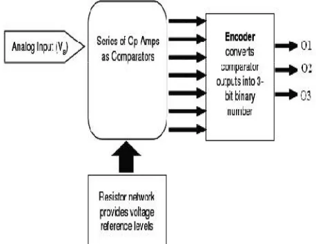
Figure 4: 3 bit Fat tree encoder
Figure 5: (a) 3-bit Fat tree based encoder, (b) Output
The logic diagram of fat tree encoder consists elementary gates such as AND, OR, NOT, EX-OR gate etc. The operation of this encoder is based on the stages of the gate and thus produces the gray code as output. The design is implemented in Tanner Tool for 3-bit, 4-bit, 5-bit encoders and the output is verified. The analysis of the various logic methods of encoder shows that the number of transistors used is high, hence the desired functionality consumes power, and area is large.
IV. PROPOSED METHOD
A. MUX BASED ENCODER
Department of ECE, Adhiyamaan College of Engineering, Hosur, Tamilnadu, India.
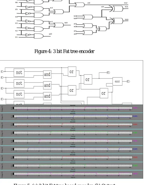
Figure 6: 2 bit MUX based encoder
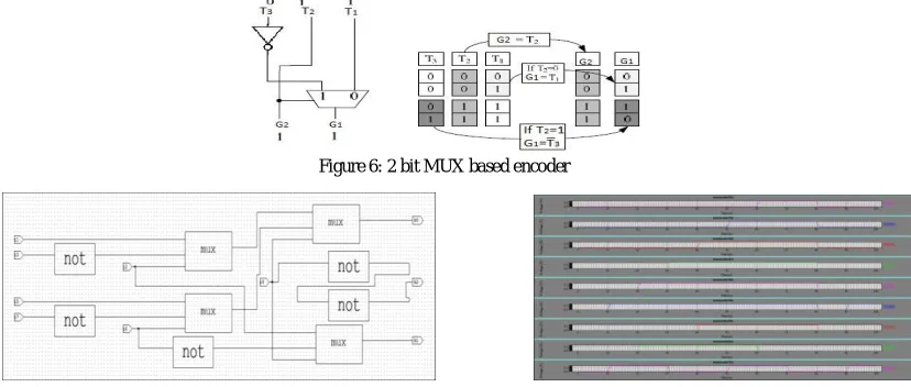
Figure 7: (a) 3-bit MUX based encoder, (b) output
V. EXPERIMENTAL RESULTS
From the analysis of designed existing logics of encoders, the MUX based encoder is the more efficient in terms of the power consumption, number of transistors, speed and ultimately the gain in area.
Table1-Comparision table
VI. CONCLUSION
To design energy efficient and a speedy encoder, the Modified MUX based encoder is proposed as an efficient design that involves reduced number of transistors with low power consumption that includes the speed while compared to other encoders.
REFERENCES
1. Mohsen Moslemi, Samaneh Babayan-Mashhadi “A Novel Power-Efficient Architecture For High-Speed Flash ADCs”- IEEE (ICEE 2014), May 20-22, 2014.
2. S. Sheikhaei, S. Mirabbbasi, A. Ivanov, "A 4-bit 5GS/s flash ND converter in 0. 1811m CMOS", in Proc. IEEE international Symposium on Circuits and Systems, 2005, pp. 6138-6141.
3. T. Sai Lakshmi, Avireni and P. Chandra Shaker, "Implementation of power efficient flash analogue-to-digital converter", IEEE Active and Passive Electronic Components International Journal(Hindawi), vol. 2014.
4. Pradeep Kumar, Amit Kolhe, “Design & Implementation of Low Power 3-bit Flash ADC in 0.18μm CMOS”, IEEE (IJSCE) ISSN: 2231-2307, Volume-1, Issue-5, November 2011.