Department of ECE, Adhiyamaan College of Engineering, Hosur, Tamilnadu, India.
Application of Data Acquisition System for
Superconducting Quantum Interface
Devices at Remote Location
Jayasudha.R1, Jeevitha.R2, Kavitha.K.G3, Mohana Priya.J.S4, Dr.S.Sathish5
UG Scholar, Department of ECE, Adhiyamaan College of Engineering, Hosur, Tamilnadu, India1,2,3,4
Professor, Department of ECE, Adhiyamaan College of Engineering, Hosur, Tamilnadu, India5
ABSTRACT: This paper works on the design of Data Acquisition for Superconducting Quantum Interface Devices (SQUID) at remote location by posting data to the Mobile Communication through GSM Module. Sensors are used to detect the variations in the parameters and send messages to analog to digital converter and the converted message is send to microcontroller, micro controller will compare input information with the max input written in the program and if any parameters cross the limit it will send a message to registered mobile through GSM module. We introduce data acquisition system that send output of superconducting quantum interface devices by means of wireless by GSM is intended to be offered. The proposed system design will make use of microcontroller within process of gathering, packing as well as sending of data. Micro controller will forward data all the way through GSM at low cost, the way we control and manage their functions would change entirely. This paper presents development of text based command processing software, output for ARM7 microcontrollers to facilitate in sending data via the cell module. The proposed design is implemented using SMS (commonly known as text message) and GSM (Internet Based Protocol) as the main communication protocol.
KEYWORDS: Superconducting Quantum Interference, Microcontroller, LPC2148 development board, GSM Module, smart phones.
I. INTRODUCTION
In this modern era research is done for data acquisition in various fields such as industrial and biomedical applications. There are many difficulties which we are facing such as complexity due to wires used for data acquisition and high power consumed in the system and these systems are expensive. Our proposed Data acquisition system based on android based application will mainly focus to improve above mentioned difficulties. We propose a system which is completely wireless and it consumes less power, it is cost effective and it is portable and it won’t be limited to specific sensor networks. This system connects mobile device with microcontroller (ARM7). Data acquisition is an important part of instrumentation. More than one node is used here in this system. Hence it is not limited to a specific set of sensors and is therefore called as Multi modal System. Also in the systems proposed earlier the output was displayed on LCD whereas we are displaying the output on an android based application like smart phone. This data acquisition system can be divided into two parts first is Hardware and second is a Software. Hardware section consists of the microcontroller ARM7 it performs the task of converting analog signals into digital one and sends it to the smart phone through SMS.
II. METHODOLOGY
Department of ECE, Adhiyamaan College of Engineering, Hosur, Tamilnadu, India.
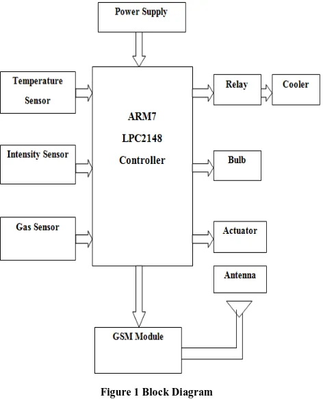
design will make use of microcontroller within process of gathering, packing as well as sending of data. Most important purpose of microcontroller is to forward data all the way through GSM. In order to integrate this interface with a home automation system, a development board with an embedded micro controller was used. The interconnection between the android and the automation system was made using a GSM Module connection. By using this GSM Module we are going to post data by sending message to smart phone.Figure 1 Block Diagram
III. WORKING PRINCIPLE
In this project Sensors are called as Super Conducting Quantum Interface(SQUID) devices. These sensors are used to detect the variations in the parameters and send messages to analog to digital converter and the converted message is send to micro controller. Micro controller will compare input information with the max input written in the program and if any parameters crosses the limit first it will display a message in the LCD after that it will send a message to registered mobile through GSM module. After the message sending operation the microcontroller will automatically execute the remedy operation for the particular situation. In this project we are using three sensors that are Gas sensor, Temperature sensor and Intensity sensor. With the help of these three sensors the physical or electrical phenomena in the area will be acquired by the data acquisition system. For example, if the temperature of the room will find high from the normal temperature the message will be send to the mobile through GSM Module and the fan will automatically rotate to cool the high temperature.
IV. HARDWARE DESCRIPTION
A. MQ7 GAS SENSOR
Department of ECE, Adhiyamaan College of Engineering, Hosur, Tamilnadu, India.
temperature, and detect CO at low temperature. It is widely used in domestic CO gas leakage alarm, industrial CO gas alarm and portable CO gas detector.4.1.1. Specifications
Operating Voltage: 3.3 – 5V. Type: Analog Sensor.
Can detect the presence of carbon monoxide
B. Lm35 TEMPERATURE SENSOR
The LM35 is an integrated circuit sensor that can be used to measure temperature with an electrical output proportional to the temperature (in °C).It can measure temperature more accurately than using a thermistor. The sensor circuitry is sealed and not subject to oxidation. The LM35 generates a higher output voltage than thermocouples and may not require that the output voltage be amplified. The LM35 has an output voltage that is proportional to the Celsius temperature.
The scale factor is .01V/°C. The LM35 does not require any external calibration or trimming and maintains an accuracy of +/-0.4°C at room temperature and +/-0.8°C over a range of 0°C to +100°C.Another important characteristic of the LM35 is that it draws only 60 micro amps from its supply and possesses a low self-heating capability. The LM35 comes in many different packages such as TO-92 plastic transistor-like package,T0-46 metal can transistor-like package,8-lead surface mount SO-8 small outline package.
4.2.1. Lm35 Features
Calibrated directly in o Celsius (Centigrade) Linear + 10.0 mV/oC scale factor
0.5oC accuracy guaranteeable (at +25oC) Rated for full −55o to +150oC range Suitable for remote applications Low cost due to wafer-level trimming Operates from 4 to 30 volts
Less than 60 µA current drain Low self-heating, 0.08oC in still air Nonlinearity only ±1⁄4oC typical
Low impedance output, 0.1 Ω for 1 mA load
C. LDR
An LDR or Light Dependent Resistor is also known as photo resistor,photocell, photoconductor.It is a one type of resistor whose resistance varies depending on the amount of light falling on its surface. When the light falls on the resistor, then the resistance changes. These resistors are often used in many circuits where it is required to sense the presence of light. These resistors have a variety of functions and resistance. For instance, when the LDR is in darkness, then it can be used to turn ON a light or to turn OFF a light when it is in the light. A typical light dependent resistor has a resistance in the darkness of 1MOhm, and in the brightness a resistance of a couple of KOhm.This is mostly used in light varying sensor circuit, light and dark activated switching circuits. Some of its applications include camera light meters, street lights, clock radios, light beam alarms, reflective smoke alarms, and outdoor clocks.
4.3.1. Advantages
Department of ECE, Adhiyamaan College of Engineering, Hosur, Tamilnadu, India.
D. LCD
LCD (liquid crystal display) is the technology used for displays in notebook and other smaller computers. Like light-emitting diode and gas-plasma technologies, LCDs allow displays to be much thinner than cathode ray tube technology. LCDs consume much less power than LED and gas-display displays because they work on the principle of blocking light rather than emitting it.An LCD is made with either a passive matrix or an active matrix display display grid. The active matrix LCD is also known as a thin film transistor display. The passive matrix LCD has a grid of conductors with pixels located at each intersection in the grid. A current is sent across two conductors on the grid to control the light for any pixel. An active matrix has a transistor located at each pixel intersection, requiring less current to control the luminance of a pixel. For this reason, the current in an active matrix display can be switched on and off more frequently, improving the screen refresh time (your mouse will appear to move more smoothly across the screen, for example).Some passive matrix LCD's have dual scanning, meaning that they scan the grid twice with current in the same time that it took for one scan in the original technology. However, active matrix is still a superior technology.
E. ARM7 LPC 2148 MICROCONTROLLER
Increasingly, embedded systems developers and system-on-chip designers select specific microprocessor cores and a family of tools, libraries, and off-the-shelf components to quickly to develop a new microprocessor-based products and applications. ARM is one of the major options available for embedded system developer.
Over the last few years, the ARM architecture has become the most pervasive 32-bit architecture in the world, with wide range of ICs available from various IC manufacturers. ARM processors are embedded in products ranging from cell/mobile phones to automotive braking systems. A worldwide community of ARM partners and third-party vendors has developed among semiconductor and product design companies, including hardware engineers, system designers, and software developers.ARM7 is one of the widely used micro-controller family in embedded system application.
ARM is a family of instruction set architectures for computer processors based on a Reduced Instruction Set Computing (RISC) architecture developed by British company ARM Holdings.
A RISC-based computer design approach means ARM processors require significantly fewer transistors than typical processors in average computers. This approach reduces costs, heat and power use. These are desirable traits for light, portable, battery-powered devices—including smart phones, laptops, tablet and notepad computers), and other embedded systems. A simpler design facilitates more efficient multi-core CPUs and higher core counts at lower cost, providing higher processing power and improved energy efficiency for servers and supercomputers.
4.5.1. LPC 2148
LPC2148 is the widely used IC from ARM-7 family. It is manufactured by Philips and it is pre-loaded with many inbuilt peripherals making it more efficient and a reliable option for the beginners as well as high end application developer.
4.5.2. Features Of Lpc 2148 Micro Controllers
• 8 to 40 kb of on-chip static RAM and 32 to 512 kb of on-chip flash program memory.128 bit wide interface/accelerator enables high speed 60 MHz operation.
• In-System/In-Application Programming (ISP/IAP) via on-chip boot-loader software. Single flash sector or full chip erase in 400 ms and programming of 256 bytes in 1ms.
• Embedded ICE RT and Embedded Trace interfaces offer real-time debugging with the on-chip Real Monitor software and high speed tracing of instruction execution.
• USB 2.0 Full Speed compliant Device Controller with 2 kb of endpoint RAM. In addition, the LPC21468 provides 8 kb of on-chip RAM accessible to USB by DMA.
Department of ECE, Adhiyamaan College of Engineering, Hosur, Tamilnadu, India.
• Two 32-bit timers/external event counters (with four capture and four compare channels each), PWM unit (six outputs) and watchdog.• Low power real-time clock with independent power and dedicated 32 kHz clock input.
• Multiple serial interfaces including two UARTs (16C550), two Fast I2C-bus(400 kbit/s), SPI and SSP with buffering and variable data length capabilities.
• Vectored interrupt controller with configurable priorities and vector addresses. • Up to 45 of 5 V tolerant fast general purpose I/O pins in a tiny LQFP64 package. • Up to nine edge or level sensitive external interrupt pins available.
• On-chip integrated oscillator operates with an external crystal in range from 1 MHz to30 MHz and with an external oscillator up to 50 MHz’s.
• Power saving modes include Idle and Power-down.
• Individual enable/disable of peripheral functions as well as peripheral clock scaling for additional power optimization.
• Processor wake-up from Power-down mode via external interrupt, USB, Brown-Out Detect (BOD) or Real-Time Clock (RTC).
• Single power supply chip with Power-On Reset (POR) and BOD circuits.CPU operating voltage range of 3.0 V to 3.6 V (3.3 V ± 10 %) with 5 V tolerant I/O pads.
F. GSM MODEM – SIM 300 (SENDING TEXT SMS)
Throughout the evolution of cellular telecommunications, various systems have been developed without the benefit of standardized specifications. This generated many problems directly related to compatibility, especially with the development of digital radio technology. The GSM standard is intended to address these problems.
This is tri-band, slim and compact so that it could be used in compact devices. Now about the hardware, it consists of a DB9 port for communicating with the computer or with the micro-controller, a jack for power, a integrated module, a connector and a micro strip antenna, an interface circuit of Max 232.To work with the modem we have to make an interfacing circuit on Max 232, which will convert the TTL logic level from the micro-controller to RS 232 level, which is 9 or 12 volts. First thing to know before working on any GSM modem is to get familiarized with the “at commands”. Embedded cellular modules(GSM Modems) are mainly controlled by the use of AT commands. AT or Attention Commands are derived from the Hayes Command set (or AT command set) from 1977 to control the 300-baud Hayes Smart modem. They are a set of command-language or instructions that are sent to a cellular module to perform different actions. Without AT commands one could not work with the modems.
4.6.1. The GSM Network
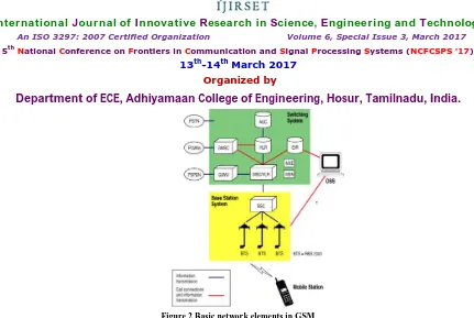
GSM provides recommendations, not requirements. The GSM specifications define the function and interface requirements in detail but do not address the hardware. The reason for this is to limit the designers as little as possible but still to make it possible for the operators to buy the equipment from different suppliers. The GSM network is divided into three major systems:
The switching system (ss) The base station system (BSS)
Department of ECE, Adhiyamaan College of Engineering, Hosur, Tamilnadu, India.
Figure 2 Basic network elements in GSM
4.6.2. The Operation And Support System
The operation and the maintenance center (OMC) is connected to all equipments in the switching system and to the BSC. The implementation of OMC is called the operation and support system (OSS).The OSS is the functional entity from which the network operator monitors and controls the system. The purpose of OSS is to offer the customer cost-effective support for centralized, regional and local operational and maintenance activities that are required for a GSM network. An important function of OSS is to provide a network overview and support the maintenance activities of different operation and maintenance organizations.
V. CONCLUSION
Department of ECE, Adhiyamaan College of Engineering, Hosur, Tamilnadu, India.
REFERENCES[1] Deniz Balaman, Ali Bozbey, “ Application of Data Acquisition System for Superconducting
Quantum Interface Devices (SQUID) at Remote Location”, in 2014 IEEE 22 Signal Processing And Applications Conference (SIU 2014) p.p.967-970.
[2] J. H. Taylor and J. M. Weisberg. Further experimental tests of relativistic gravity using the binary pulsar psr 1913+16. The Astrophysical Journal, 345:434, 1989.
[3] Allegro energy spectrum for 1991, 1993 and 1994. The bottom scale gives the signal threshold in Kelvin, the top scale gives the signal threshold in terms of the burst strain amplitude of a gravity wave incident with optimum polarization and direction.
[4] H. J. Paik. Ph.D. Dissertation. Stanford University, 1974.
[5] N. Solomonson, W. O. Hamilton, and W. Johnson. Construction and performance of a low noise inductive transducer for the Louisiana State University gravitational wave detector. Rev. Sci. Instrum., 65(1):174, 1994.
[6] A. V. Oppenheim and R. W. Schafer. Digital Signal Processing. PrenticeHall, 1975.
[7] L. A. Wainstein and V. D. Zubakov. Extraction of Signals from Noise. Dover Press, New York, 1962. [8] A. D. Whalen. Detection of Signals in Noise. Academic Press, New York and London, 1971.
[9] S. Boughn et al. Method for calibrating resonant-mass gravitational wave detectors. Rev. Sci. Instrum., 61(1):1, 1990.