AN-TE DENG. Flexible ASIC Design using the Block Data Flow Paradigm (BDFP). (Under the direction of Dr. Winser E. Alexander and Dr. Clay S. Gloster.)
An Application Specific Integrated Circuit (ASIC) outperforms most processors; however, it is limited to one algorithm. Instruction Level Parallelism (ILP) processors, which include mixed type processors such as the Digital Signal Processor (DSP), the Very Long Instruction Word (VLIW) Processor, the Reduced Instruction Set Computer (RISC), and the Complex Instruction Set Computer (CISC), are popular due to their flexibility and programmability. Thus, they can be used for many different applications. However, their cost-performance can not meet the needs of many real world applications.
In this research, we mapped three different algorithms, the one-dimensional Finite Impulse Response (1D-FIR), the two-dimensional Finite Impulse Response (2D-FIR), and the two-dimensional Infinite Impulse Response (2D-IIR) filter into the same flex-ible hardware architecture using the Block Data Flow Paradigm (BDFP). The idea of a Flexible Application Specific Integrated Circuit (FASIC) is to design a mixed architecture using an ASIC for the fixed part of the system while using a Field Pro-grammable Gate Array (FPGA) for the part of the system that requires a change of parameters for different algorithms. The Block Data Flow Parallel Architecture (BDPA) design, which has near super computer performance for media processing, is meant to form part of the FASIC library (Intellectual Property, IP) and is to be integrated with a general purpose host computer or mixed processor computer as an accelerator.
To my beloved wife,
Vicky,
and my two children,
BIOGRAPHY
ACKNOWLEDGEMENT
But they that wait upon the LORD shall renew their strength; they shall mount up with wings as eagles;
they shall run, and not be weary;
and they shall walk, and not faint.
Isaiah 40:31
I thank God who gave His inspiration to me while I was in despair at the last stage of my research. I could not have completed this research without His companionship. I would like to thank Dr. Winser E. Alexander for his patient mentoring, for his encouragement, and for his keen insights that have supported me through out my research and thesis writing. I would also like to thank Dr. Clay S. Gloster, Jr. for his generous advice and help. I also thank Dr. Paul D. Franzon and Dr. Zhilin Li for their assistance throughout my dissertation research.
Contents
List of Figures vii
List of Tables ix
1 Introduction 1
1.1 Instruction Level Parallel Processor . . . 2
1.2 Algorithm-Hardware Architecture Mapping Processor . . . 3
1.3 Contribution . . . 6
2 Previous Work 8 3 Block Data Flow Paradigm 14 3.1 Block Data Parallel Architecture (BDPA) . . . 15
4 Hierarchical Data Flow Control Concept 18 5 Dual Clock Rate Multi-processor System 22 6 Algorithm Partitioning and Mapping 26 6.1 1D-FIR Filter Algorithm . . . 26
6.2 2D-FIR Filter Algorithm . . . 28
6.3 2D-IIR Filter Algorithm . . . 30
7 Architecture Mapping and Design 33 7.1 Commonality and Differences between Algorithms . . . 33
7.1.1 Commonality . . . 33
7.1.2 Differences . . . 34
7.2 Input Module Architecture . . . 35
7.2.1 1D-FIR Filter . . . 35
7.2.2 2D-FIR Filter . . . 38
7.2.3 2D-IIR Filter . . . 45
7.3.1 1D-FIR Filter . . . 45
7.3.2 2D-FIR Filter . . . 48
7.3.3 2D-IIR Filter . . . 63
7.4 Output Module Architecture . . . 71
8 Scalability and Flexibility 72 8.1 1D-FIR Filter . . . 72
8.1.1 Scalability . . . 74
8.1.2 Flexibility . . . 75
8.2 2D-FIR Filter . . . 77
8.2.1 Scalability . . . 77
8.2.2 Flexibility . . . 79
8.3 2D-IIR Filter . . . 80
8.3.1 Scalability . . . 81
8.3.2 Flexibility . . . 82
8.4 Interchangeability between Algorithms . . . 83
9 Design Methodology 85 10 Performance Analysis 88 10.1 2D-IIR Filter . . . 88
10.2 1D-FIR Filter . . . 89
10.2.1 Waveform Comparison . . . 89
10.2.2 Throughput Performance . . . 93
10.3 2D-FIR Filter . . . 95
11 Conclusion 97 Bibliography 99 A Simulation Signal Waveforms 104 B Control Pseudo Codes 111 B.1 2D-FIR Filter System . . . 111
B.1.1 IM Control . . . 111
List of Figures
3.1 Block Data Parallel Architecture . . . 16
4.1 System Top Level Block Diagram . . . 19
4.2 Processor Module Array Block Diagram . . . 20
5.1 2D-FIR Filter Data Flow Bottleneck . . . 23
6.1 Signal Flow Graph of 1D-FIR Filter Direct Implementation . . . 27
6.2 2D-FIR Filter Signal Flow Graph . . . 29
6.3 Second Order 2D-IIR Filter Signal Flow Diagram . . . 31
7.1 Overlapped Block Graph . . . 35
7.2 FIFO Distribution Sequence . . . 36
7.3 Input Module Block Diagram . . . 37
7.4 2D Overlapped Image with FIFO Index . . . 38
7.5 2D Overlap Image . . . 39
7.6 2D-FIR Filter Image Preprocessing Block Diagram . . . 41
7.7 Processor Block Diagram . . . 45
7.8 Token Switch Block Diagram . . . 47
7.9 Sub-block Data Distribution . . . 50
7.10 Row-processor Example . . . 51
7.11 2D-FIR Filtered Image using Floating Point Computation . . . 53
7.12 2D-FIR Filtered Image using One-section Computational Primitive Operation . . . 54
7.13 Four-section Computational Primitive Signal Flow Graph . . . 55
7.14 Four-section Computational Primitive Finite State Machine Controller 57 7.15 2D-FIR Filtered Image using Four-section Computational Primitive processing . . . 58
7.16 Sub-image Data Block . . . 62
7.17 2D-IIR Computational Primitive . . . 64
7.18 2-D IIR Processor Block Diagram . . . 66
9.1 Simulation Environment Block Diagram . . . 85
10.1 1D Original Signal . . . 89
10.2 1D Signal with Noise . . . 90
10.3 Matlab Filtered Output . . . 91
10.4 1D- FIR Filtered Output . . . 92
10.5 1D-FIR Filter Performance . . . 94
10.6 2D-FIR Filter Performance . . . 95
A.1 One Frame Image Processing Waveforms . . . 104
A.2 One Frame Image Processing Waveforms . . . 105
A.3 Example of First Processor Idle Time . . . 106
A.4 Example of First Processor Idle Time . . . 106
A.5 Row-block Number Waveform . . . 108
A.6 Row-block Number Waveform . . . 108
A.7 Output Row-block Number Waveform . . . 109
A.8 Output Row-block Number Waveform . . . 109
A.9 Output Row-block Value Waveform . . . 110
List of Tables
7.1 2D-IIR State Table for State Variable Equations . . . 66
8.1 1D-FIR Filter System Variable Parameters . . . 74
8.2 2D-FIR Filter System Variable Parameters . . . 78
8.3 2D-IIR Filter System Variable Parameters . . . 81
10.1 2D-IIR Performance Table . . . 88
Chapter 1
Introduction
The on-the-fly image processing system is embedded on an air-borne or a sea-borne vehicle. The image processing for this kind of system demands powerful computing performance in the range of 1 GFLOPs/s to 50 TFLOPs/s [19]. The solution to this real world demand is not only a high performance FASIC but also a small size and low power consumption system.
G. E. Moore has been recognized for the derivation of a law that has been valid for the past 20 years [4]. The density of integrated circuits increases at a rate of 50% every year, hence quadrupling every 3.5 years [5]. At the same time, the peak clock speed of the circuits doubles every three years.
Scientists in New Mexico have successfully transported an atom’s nucleus from one area in a molecule to another without moving matter [27]. It is stated that this achievement, in which subatomic information was controlled and processed, could lead to extremely high-speed subatomic-based computers and communications systems. Also, physicists at MIT have announced that they have successfully controlled the atom in a laser-like stream [21]. It is called an atom laser. The laser has a much smaller wavelength than that of typical CO2 lasers used in industry. The third, recently unveiled Extreme Ultraviolet Lithography technology [11], gives a hope to render a processor that is ten times faster in the near future. All these discoveries give strong indication that Moore’s law will continue to be correct for the next decade.
with different algorithms on a single chip, will finally come true in the near future. The developing technologies mentioned above give certain confidence that there will be a great demand for system-on-chip design, which at present has a bottleneck due to the current scarcity of talented designers [25, 30].
The industry recently has been anxious to integrate many handy applications such as real-time voice/image communication, internet surfing, games, personal housekeep-ing management, and other functions together in one wireless hand-held machine. This information technology expansion and the demand for real-time image trans-mission have provided motivation for designers to develop faster and more efficient computers and coprocessors. As a result, the multi-processor, DSP chip, ASIC, par-alleling instructions, Single Instruction Multiple Data (SIMD), and Multiple Instruc-tion Multiple Data (MIMD) technologies have been implemented in attempts to solve these demanding computational problems.
1.1
Instruction Level Parallel Processor
In order to solve a computational-intensive problem in real-time, a designer would normally use one of two methodologies. The first one is to use available technol-ogy, which is more traditional, more general purpose, and more popular. We call it Instruction Level Parallelism (ILP) computation. One would select the mathemati-cal representation of an application, program it with a popular high level computer language (i.e., C, C++), which normally uses sequential operations, and identify the parallelism in the program instruction code for mapping the application to a multi-processor/multifunctional unit system at a later point. This kind of design normally can be found in embedded system, Hardware/Software (HW/SW) co-design system, and multimedia processors.
pro-cessing latency and therefore decreases the system performance. The design process and the control mechanism for the ILP system are complex whether using a special compiler or manually decoding the instruction to investigate the loop parallelism. The cost-performance of the ILP system is normally low and not efficient [14].
1.2
Algorithm-Hardware Architecture Mapping
Pro-cessor
The second approach, which is implemented in this research, is to start the de-sign by partitioning the input data geometrically and identifying the parallelism in the mathematical algorithm at the same time. The optimized and partitioned small algorithms are then mapped into a multiprocessor system. In December, 2000 [15] Kurt Keutzer et al. asserted that it is not a good approach to worry about hard-ware/software boundaries without considering higher levels of abstraction. They emphasize that capturing a design at higher levels of abstraction generates better designs in the end. They also believe that the most important point for functional specification is the underlying mathematical model. The concept that is empha-sized by Kurt Keutzer has been carried out in the design process in this research. The mathematical algorithm partitioning, data allocation, data-processor path man-agement, and concurrent data processing are considered simultaneously at the early design stage [14, 20]. This algorithm mapping, hardware architecture design method-ology starts with understanding the application’s arithmetic operations and its data path characteristics, and then continues with developing the proper architecture or micro-architecture specifically for its operation. This design methodology is also a future focus work mentioned by Kurt Keutzer’s team [15]. The 2D-FIR filter system designed in this paper has a two-level hierarchical processor architecture. The hierar-chical processor architecture, with each processor having an on-board FIFO memory and hierarchical data path control, is the new architectural design trend for the VLIW system. This concept has recently been proposed by Jacome and Veciana [14].
not possible. The traditional ASIC is designed specifically for only one application. The objective of this paper is to use the same piece of mixed ASIC/FPGA hardware to accommodate three different algorithms. The special feature in our research is that, although the designed system is a mixed ASIC/FPGA hardware system, the system can be configured into another algorithm architecture which runs a different functional operation by changing several parameters or a few modules in the processor core. This same hardware is not only scalable but also generates near supercomputer throughput performance. In order to reach this goal, we have divided our task into two parts. The first part is to solve the data flow bottleneck problem, which includes the data block formatting operation, data flow control, and asynchronous but concurrent data block processing. The second part is to design the processor core for three different algorithms with the effort of minimizing the variation of the processor architecture.
A one dimensional or two dimensional media signal normally is transmitted in a bit stream pattern. This bit stream data source, according to the algorithm that is in use, is first transformed into a proper blocked data format. All three algorithms presented in this research have their own blocked data format. We have designed a special Input Module (IM), its distribution module controls the input data format and it is reconfigurable to accommodate three different algorithms. A two way regulator is designed in the IM to control the data flow and to provide sufficient data for the processors. It monitors the data flow and handshaking with both the data source and the processor array.
characteristic of the BDPA when the data flow bottleneck problem was solved by using the dual clock rate multiprocessor system.
In order to avoid clock skew, which normally happens in a systolic array sys-tem, and to avoid connection delay (as opposed to the traditional gate delay [30]), which easily happens in a deep sub-micron system on chip design, we developed a hierarchical asynchronous data flow control architecture. This architecture has the asynchronous data driven property, which satisfies the high performance computing, linear speedup BDFP basic requirements. It also accommodates a system with dual clock rates. If an asynchronous circuit is implemented in the system, the power con-sumption of the system will be lower than it would be with the normal synchronous one [10]. The asynchronous circuit system is more resistant to magnetic interference when the system clock frequency goes higher. The concurrent operation, through-put performance, and the efficiency for the asynchronous data driven system are also higher [10].
The dissertation presents the one dimensional finite impulse response (1D-FIR) filter, the two dimensional finite impulse response (2D-FIR) filter, and the two di-mensional infinite impulse response (2D-IIR) filter designs as examples to explain the innovation of the block data flow paradigm. We have shown that this systematic algorithm mapping architecture design methodology can be implemented for differ-ent algorithms. The dissertation begins with the mathematical represdiffer-entation of the algorithm and considers different implementation schemes that can be used with a multiprocessor system. Secondly, it presents a way to partition the mathematical equations in order to simplify data access at the processor level. It discusses various architectures in the algorithm mapping process with a goal of obtaining a simple, flexible parallel architecture. Lastly, it describes a way to develop different algo-rithms that can fit in the same hardware without changing too many architectural parameters.
processing mechanism to form the BDFP. This dissertation starts with the introduc-tion, which emphasizes that the designed architecture of the BDPA matches with the trend used for many media/embedded processors. The second chapter gives a his-tory of the previous related work. The characteristics of the BDFP, the basic block diagram of the BDPA and its function are introduced in chapter three. Chapter four explains a new hierarchical data flow control (HDFC) architecture. It describes the advantages of the HDFC and how a simple HDFC is implemented in the BDPA. Chapter five introduces a dual clock rate multiprocessor system concept and how it solves the data flow bottleneck problem in the BDPA. Chapter six describes the three algorithms that we present in this paper. Chapter seven addresses the data partitioning, the hardware architecture design and mapping. Chapter eight empha-sizes the scalability and flexibility of our system architecture. It describes both the architectural difference between different algorithms and the variability within the architecture itself. Chapter nine introduces the design methodology we used and its validation. Chapter ten analyzes the performance of the three designed systems. The last chapter addresses our conclusions and future potential work.
1.3
Contribution
The purpose of this research is to map different algorithms on the same mul-tiprocessor hardware. Several contributions were discovered/developed during the research.
• Three different algorithms have been successfully mapped onto the same hard-ware multiprocessor architecture.
• The flexibility and scalability of the hardware has been proven.
• A hierarchical data flow control and a hierarchical processor architecture (HPA) have been introduced.
• High throughput performance and the large scale linear speedup characteristic of the BDPA have been validated.
• A neat algorithm mapping and hardware architecture design research environ-ment has been introduced to the High Performance Computing Laboratory at North Carolina State University.
• A remote real-time reconfigurable multi-function system concept has been in-troduced.
Chapter 2
Previous Work
Pierpaolo, et al., selected five versions of RISC workstations to demonstrate their image processing capability in 1996 [9]. Some source inefficiencies were found after a preliminary set of experiments.
• The intensive computing parts of Image Processing and Pattern Recognition (IPPR) programs are organized as processing loops of limited size. In such pieces of code, the loop control processing overhead takes up most of the total processing time.
• The iterative organizations of IPPR programs generate many data dependency problems in pipelined architectures.
• Image processing and pattern recognition programs have specific functional units (e.g., integer/floating point units). RISC machines have different data paths (e.g., from integer to floating point registers and vice versa). The use of the data types that naturally match the task characteristics in the source programs may turn out to be an un-optimized solution.
both on the characteristics of the host architecture and on the compiler used.
• The choice of a specified order in input data structures (e.g., the images) allows defining program and data partitioning strategies. Their strategies depend on the size of the cache memory and are aimed at reducing the average latency of memory accesses.
The inefficiencies mentioned above exist for most traditional general purpose comput-ers. As the computer-oriented modifications (i.e., partitioning the existing program into larger parallel loops, arranging the pre-computed variables in a way easier to be accessed) are made, problems associated with the compiler, data accessing and I/O contention still exist.
Hammerstrom and Lulich developed a one-dimensional SIMD (1D-SIMD) proces-sor array with the precision of 8-bit fixed point in 1996 [12]. This 1D-SIMD chip was specially designed for image processing and pattern recognition. Bit-parallel arith-metic was used because programming it is easier and faster for high precision. On-chip or off-chip memory was reviewed and the system used on-chip memory. Nevertheless, the system had the following weaknesses:
• An 8-bit input/output port was used, making it inadequate for many applica-tions.
• More on-chip taps were needed to provide more buffering for more processors.
• A more powerful, data-driven, barrel shifter was needed in the processor.
• A simpler, register-register RISC-like instruction set needed to be developed in order for the compiler to generate code easier.
have limited parallelism at the instruction level. Second, as the parallelism increases, the wiring connectivity required on the VLIW chip increases due to the use of a single global register file and the global crossbar network. This wiring becomes a performance-limiting factor. Third, as the internal instruction bandwidth increases, the I/O capacity increases as well. Small cache miss rates will lead to significant stall on executing the instructions. Fourth, the ability of compilers to schedule multiple threads onto a single VLIW stream is poor. In order to improve performance on an instruction level parallelism architecture, Kneip concludes that VLIW methodology will have to make the best use of the algorithm’s parallelization potential. This leads to the need for implementing additional levels of parallelism, especially the use of data and task parallel processing. This conclusion is consistent with the concept of the BDFP. That is, the data should be partitioned in blocks and processing should be done with parallel pipeline processors.
The special Very Long Instruction Word (VLIW) Application Specific Instruction-Set Processor (ASISP) was proposed by Margarida F. Jacome et al. in 2000 [14]. The research emphasized adding as much functionality as possible to embedded soft-ware in order to meet the demand of designing complex systems within the short time-to-market windows. The traditional memory accessing problem with VLIW was addressed and a distributed memory solution was proposed. The VLIW ASISP architectural design direction was described in detail, which is very similar to the actual architecture of the FASIC. Data partitioning, memory allocation and assign-ment, scheduling of data operations, loop transformations, and other complex tasks were mentioned in the research. A library of hierarchically parameterized fundamen-tal components was also proposed. The ongoing research for VLIW ASISP involves studying in more detail specific algorithms, data partitioning schemes, effective mem-ory synthesis systems, and powerful optimizing compilers.
micro-processor architecture, which was stated as one of their future interest.
Giobanni De Micheli et. al. published their research in “Hardware/Software Co-Design” in March, 1997 [20]. The paper discussed the defects that normally result during the design procedures for hardware/software co-designers. It is very common to design a system starting from applying task partitioning before thinking of schedul-ing/binding with the resource. This kind of design approach only introduces the loss of parametric accuracy, and the final result is not controllable. Only concurrently performing the task partitioning, scheduling, and binding to resources will generate an optimal resource utilization result. This paper gave us inspiration for designing the FASIC in that the data flow bottleneck, processing bottleneck problem, and limited resources should always be in mind when designing any module in the FASIC system. The rapid prototyping of application specific signal processors (RASSP) program started in 1993 and ended in 1998 and was managed by the DARPA Electronics Technology Office. The program concentrated on improving the process for devel-oping high-performance embedded digital signal processors. Four benchmarks were used during the five year RASSP program. They were Synthetic Array Radar (SAR) Image Processor (Benchmarks-1 & 2), Upgrade of an Embedded Sonar Processor (Benchmark-3), and Upgrade of an Embedded Image Enhancement Processor and ATR (Benchmark-4). The C and VHDL simulators of the SAR Image processor were available for companies and individual personal, but not for the public. The proces-sors were basically integrated with Commercial Off The Shell (COST) components, such as DSP chips, micro-processors, and FPGAs. The tools used were upgraded from time to time. Graphical programming and auto-code tools were used for signal processing applications. Functional analysis of system requirements was carried out and resulted in a reduction of the number of operations in the image enhancement code by 2.8 times, and in the pattern matching code by 2.4 times. A 20 chip/second demonstration was achieved. A chip represents a 79 x 79 pixel sub-image.
architecture. Digital filtering algorithms using a parallel block processing method were introduced in the early 1990s [29]. A ring type network, 1D processor array was investigated.
Xu and Alexander introduced the criteria for mapping algorithms into the BDFP [36]. The data partitioning, as well as algorithm-partitioning concept, was empha-sized. A block data flow parallel architecture (BDPA) block diagram was formed. The concept of block data flow, the data transmission protocol, the linear array topology, the skew-operation, and the I/O data communication were discussed. A functional level simulation demonstrated that the expected performance of a BDPA system is very promising.
Since the BDFP has matured, several signal processing applications and matrix operation have used this concept to form a BDPA and each has obtained very promis-ing performance. Wilburn [33] developed the algorithm partitionpromis-ing for the Dis-crete Wavelet Transform (DWT) and applied the BDPA to real-time occluded object matching [35]. Yoon [37] extended this to a 2-D DWT architecture block diagram design. Howard [13] applied the BDFP to the Kalman filter and developed a mod-ularized BDPA to solve the weather problem. Wilburn [34] also used the BDFP to develop a parallel solution for solving systems of linear equations. A systematic evolution of the BDFP, including an order graph method responsible for processing scheduling, was introduced by Alexander et. al. [2].
Chapter 3
Block Data Flow Paradigm
The Block Data Flow Paradigm (BDFP) involves partitioning data into large granularity blocks, scheduling and processing the data within different processors in which partitioned algorithms are embedded. The Block Data Parallel Architec-ture (BDPA) is an example of the implementation of the BDFP [2]. It reduces the communication overhead problem between memory and processors. It uses the asyn-chronous data flow characteristic so that the control overhead is reduced. The data communication time is overlapped with the computing time. Therefore, it gives high performance. The BDPA adopts the 1D linear array pipeline characteristic so that the system utilization is very high and easy to scale up. The number of input/output pins per-processor will not increase as the number of processors increases. The power dissipation is lower than for the 2D array system, yet the performance is similar [12]. The BDPA has the following special characteristics:
• Different but similar DSP application algorithms are studied and broken down into small parallel processes.
• The small algorithmic parallel processes are translated into small programs and installed into different processors.
• The processors are arranged in a one directional linear array pipeline.
• The hierarchical data flow control concept is implemented to enable individ-ual processors to operate concurrently and asynchronously. The processing of a block begins as soon as it is available. No global control or complicated schedul-ing is needed to indicate the explicit start and stop times for block processschedul-ing.
• Each processor computes the output derived from its assigned input block and transmits this output to the output device as soon as it is ready.
• Partial or intermediate results, which must be exchanged between processors, pass through a point-to-point simple (single stage) interconnection network.
3.1
Block Data Parallel Architecture (BDPA)
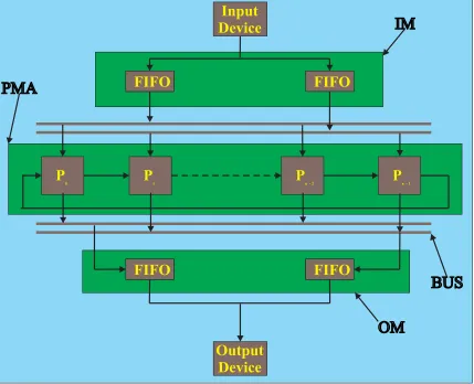
The theme of the BDPA is to process the data in large granularity blocks. We developed the BDPA to implement the BDFP for a variety of one-dimensional and two-dimensional DSP applications. The architecture is composed of three main parts, the Input Module (IM), the Processor Module Array (PMA), and the Output Module (OM) in order to manage the block flow smoothly through the processors.
In figure 3.1, the IM receives the data string coming from the input device. The input device could be an audio/video recorder, a sound/graphic file installed on a disk, or a host system data file. The IM acts as an I/O buffer which splits and forms the incoming data string into data block format. It has a distributor at the front end so that the data blocks can be distributed into the corresponding FIFO buffer. The FIFO outputs transfer data blocks into each of the different processor modules in a direct individual channel without any interference. A data flow regulator is responsible for handshaking at both sides of the IM, which is the input device and the PMA.
input channel and an output channel. The processors are divided into two processor groups, namely, an odd number processor group and an even number processor group. Each processor group is directly connected to one of the input FIFO buffers and one of the output FIFO buffers. The purpose of dividing the processors into two groups is to make sure that the two IM FIFO buffers alternatively write and read at the same time. The individual processor will process its own mathematical operations (small programs) on the data and update the values inside itself until the whole block of data is finished. The partitioned algorithm and the partitioned data determine the number of iterations within a block. The intermediate values from each processor are transferred to the FIFO between the processors as needed according to the algo-rithm being implemented. The transferring of the intermediate values is only in one direction. The calculated output value of each processor is output sequentially to the FIFO in the OM.
Chapter 4
Hierarchical Data Flow Control
Concept
Traditional processor control normally uses a centralized control technique which is designed with complex scheduling schemes, such as interrupt, queue, semaphores, round robin. When the system grows larger, it is very difficult to synchronize the multi-tasking.
the asynchronous design renders more concurrent operations and higher efficiency (average-case performance as opposed to worst-case performance). When the system design gets more and more complicated and different function modules are integrated for a system on a chip using deep sub quarter micron silicon, the timing delay problem between different connected modules will get more serious. An asynchronous HDFC, modularized design, will eliminate a lot of these potential problems [30].
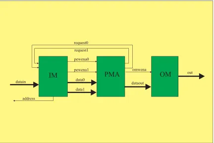
Figure 4.1: System Top Level Block Diagram
The IM FIFO guarantees adequate data block are provided for the PMA. Only when both of the IM FIFOs are full will the IM regulator, which monitors the IM FIFOs status, fire a freeze signal to stop the data coming from the data source. Therefore, the regulator control signal is determined by the data flow situation.
In figure 4.1, the signals exchanged between the IM and the PMA are the request signals, the data buses, and the FIFO write enable signal lines. The only active (as opposed to passive) signal generated from the PMA to the IM is the data request signal. This signal will stay alive until one block of data is fed into the requesting processor. There will be no request signal if all the processors are busy. Other than the request signal, the PMA has no control over the data flow.
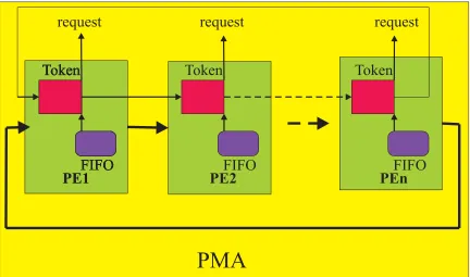
Figure 4.2: Processor Module Array Block Diagram
un-til the block of data is output to the OM. The processor architecture itself can be hierarchical. Whether it is one level processing or two level hierarchical processing depends on the algorithm. The algorithms we use have architectures with no more than two hierarchical levels. Therefore, the hierarchical processing controller is easily implemented in our system with a variable counter combined with a finite state ma-chine controller. The controller follows the data processing cycles, controls the data processing flow, data path, and feeds the data back to the processor FIFO.
Since the data block assignment (the path of the data block) is controlled by the token passing controller, there is no need for complex task scheduling, synchronizing controllers, or complex data path assigning. Thus, the PMA is a self-sufficient control, pipeline parallel processing, one dimensional linear array, and is a fully data block driven module.
Chapter 5
Dual Clock Rate Multi-processor
System
Linear speedup and high throughput performance are the goals and characteristics of a BDPA. In order to reach these goals, it is necessary to provide the processors with sufficient data and keep them busy at all times. However, most of the time, a multiprocessor system bottleneck occurs either due to the speed of the data bus or instruction scheduling (i.e., branch prediction). We categorize this kind of bottleneck as the data flow bottleneck. This data flow bottleneck will saturate the multiprocessor operation and prevent the system from obtaining any more speedup. In other words, no matter how many processors are added to the multiprocessor system, there is no increase in throughput.
OM was done to reduce the data flow bottleneck problem. The use of a dual rate clock multiprocessor can further reduce this problem.
Figure 5.1: 2D-FIR Filter Data Flow Bottleneck
A data flow bottleneck example is shown in figure 5.1. The signal waveforms in row 8 and row 9 in figure 5.1 are the PMA request signal. The normal operation is to provide a processor its requesting data block whenever it raises a request signal. This normal operation is also the basic principle for a BDPA to have the linear speedup characteristic and high throughput performance. Now, the request signal is suspended after five processors obtain their data blocks. We were using six processors for this simulation. That means the IM FIFO is not big enough and is already empty before the sixth processor tries to obtain its data block for the first time.
The algorithm we used in our design for the FIR filter system is the overlap-save algorithm. With this algorithm, there is an overlapped area for each data block. Be-fore the data block is input into the PMA, the overlapped data block must be formed. While this data block is formed, in the 1D-FIR filter system case, the overlapped area data is broadcast to both IM FIFOs simultaneously. In order to let the PMA acquires its data block first, during this broadcasting time, the data source is stopped because the FIFO cannot be read and written to at the same time. This data flow bottleneck is an unavoidable situation with the 1D-FIR filter system unless the data blocks are formed outside of the system in advance.
will still be empty. The second solution is changing the FIFO memory into dual port RAM memory, since dual port RAM can be read and written to at the same time. However, the read/write controller for the dual port RAM must not read and write at the same address at the same time. The read/write controller itself is another complicated design and consumes much of the wafer area and power.
A third solution is to use the dual clock rate multiprocessor system. The procedure of using a dual clock rate system is to use a very high clock rate to acquire the data block, process the data at the slower clock rate required in the processor, and output the processed data block from the processor FIFO to the OM at the original high clock rate. Since system clock rates are increasing at a very fast pace, it is simple and easy to add a clock divider in our design to implement the dual clock rate multiprocessor system to obtain high throughput performance. This method is better than adding complicated control circuitry or a large memory to the system. The linear speedup performance of the whole system was improved dramatically by using a dual clock rate multiprocessor system.
The BDPA processor architecture and its HDFC architecture are well designed to accommodate globally asynchronous, locally synchronous processing, and it is totally modularized. After the processor gets its own data block, it is isolated from the outside environment. The only interface of a processor to the outside environment is the on board FIFO. Therefore, it is feasible to use the system clock, which is faster, to input/output the data block into/from the on board processor FIFO while using another slower rate clock to drive the data through the processor computational primitives.
the data block buffer but without actually adding any memory or a complicated con-troller in the system circuitry. We can call it a phantom memory. The data flow speed to the data processing speed ratio is adjustable. Therefore by adjusting this ra-tio and adjusting the number of processors in the system, we can obtain the targeted performance and processor utilization for the BDPA.
Chapter 6
Algorithm Partitioning and
Mapping
The purpose of partitioning the algorithm is that the partitioned task can be run on different processors concurrently. This is different from parallelizing a sequential program and running it on a super computer, or parallelizing the instructions and running them on a general-purpose computer with VLIW technology. The algorithm partition strategy for the BDFP starts partitioning at the mathematical equation level while the other parallelism methods are based on the program or instructions. Note that the program or the instruction itself is normally sequential and follows a Von Neumann architecture in nature. Therefore, the cost-performance of the BDFP is expected to be better than that of the other methods.
6.1
1D-FIR Filter Algorithm
The transfer function of a 1D-FIR filter is
H(z) = Y(z)
X(z) = L
k=0
b(k)z−k, (6.1)
where Y(z) is the Z–Transform of the output data and X(z) is the Z–Transform of the input data. L is the filter order and b(k) represents the filter coefficients. z−k is the kth delay element. The transfer function can then be expanded as
Y(z) = L
k=0
b(k)X(z)z−k, or
Y(z) = b(0)X(z) +b(1)X(z)z−1+b(2)X(z)z−2+· · ·+b(L)X(z)z−L. (6.2) The equation above does not give us much information on parallelism; it only describes an input data multiplied by all the designated filter coefficients with designated delays. However, if we use a simple direct implementation for the equation, the difference equation can be easily represented with the following signal flow graph in figure 6.1.
Figure 6.1: Signal Flow Graph of 1D-FIR Filter Direct Implementation
state variables can be stored in these registers and subsequently used for the next computation iteration. Therefore, it is more logical to locate the state variables at the input of the delays.
According to the signal flow graph and the assignment of the state variables, the state variable equations are as follows:
qL(n) = b(L)x(n)
qL−1(n) = b(L−1)x(n) +qL(n−1)
qL−2(n) = b(L−2)x(n) +qL−1(n−1) ..
.
q1(n) = b(1)x(n) +q2(n−1)
y(n) = b(0)x(n) +q1(n−1). (6.3)
6.2
2D-FIR Filter Algorithm
We also start our 2D-FIR filter system design by partitioning the mathematical equation, trying to optimize these equations in a sense of parallelism, and mapping the parallel smaller tasks into different processors. At the same time, we need to consider the partitioning of an image into blocks of data that can flow smoothly through our processors.
The 2D-FIR transfer function is
H(z) = Y(z1, z2)
X(z1, z2) = L2 k2=0 L1 k1=0
b(k1, k2)z1−k1z2−k2, (6.4) where X(z1, z2) is the transform of the input image data, Y(z1, z2) is the transform of the output result, b(k1, k2) represents the filter coefficients, and z1−1 and z2−1 are horizontal and vertical delay elements. The filter is L1 + 1 by L2 + 1 in size. The order is L1 by L2 . If we separate the input and the output transforms on different sides of the equation, we obtain
Y(z1, z2) = L2 k2=0 L1 k1=0
It is not so easy to see any parallelism with the difference equations. Therefore, we expand the difference equation into a two-dimensional signal flow graph as shown in figure 6.2.
Figure 6.2: 2D-FIR Filter Signal Flow Graph
From figure 6.2, we can compute the present cycle state variable and store it into the delay element for the usage of the next cycle state variable. Therefore, the state space representation of the signal flow graph and the output equation is
y(n1, n2) = x(n1, n2)b(0,0) +q1,1(n1−1, n2) +q2,1(n1, n2−1)
q1,1(n1, n2) = x(n1, n2)b(1,0) +q1,2(n1−1, n2)
q1,2(n1, n2) = x(n1, n2)b(2,0) +q1,3(n1−1, n2) ..
q1,L(n1, n2) = x(n1, n2)b(L,0)
q2,1(n1, n2) = x(n1, n2)b(0,1) +q1,L+1(n1−1, n2) +q2,2(n1, n2−1)
q1,L+1(n1, n2) = x(n1, n2)b(1,1) +q1,L+2(n1−1, n2)
q1,L+2(n1, n2) = x(n1, n2)b(2,1) +q1,L+3(n1−1, n2) ..
.
q1,2L(n1, n2) = x(n1, n2)b(L,1)
q2,2(n1, n2) = x(n1, n2)b(0,2) +q1,2L+1(n1−1, n2) +q2,3(n1, n2 −1)
q1,2L+1(n1, n2) = x(n1, n2)b(1,2) +q1,2L+2(n1−1, n2) ..
.
q2,L(n1, n2) = x(n1, n2)b(0, L) +q1,L(L−1)+1(n1−1, n2)
q1,L(L−1)+1(n1, n2) = x(n1, n2)b(1, L) +q1,L(L−1)+2(n1−1, n2) ..
.
q1,L(L−1)+L(n1, n2) = x(n1, n2)b(L, L) (6.6) The dashed square in figure 6.2 shows a possible computational primitive to be used to implement the filter.
6.3
2D-IIR Filter Algorithm
The third algorithm that is used in this paper is a second order 2D-IIR filter system. It is also a filtering algorithm, but the data computation itself is different from the previous two.
The transfer function of a 2D-IIR filter is
H(z1, z2) =
L1 j1=0 L2 j2=0
b(j1, j2)z1−j1z2−j2
1 + L1 j1=0 L2 j2=0
a(j1, j2)z1−j1z2−j2
j1+j2>0
The example we use is a second order 2D-IIR filter, whereL1 =L2 = 2. The transfer function is expanded as
Y(z1, z2) = b(0,0)X(z1, z2) +
2
j1=0
2
j2=0
[b(j1, j2)X(z1, z2) j1+j2>0
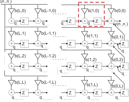
− a(j1, j2)Y(z1, z2)]z−1j1z−2j2, (6.8) and is represented in a two dimensional signal flow graph as shown in figure 6.3, where
x(n1, n2) is the input pixel data and they(n1, n2) is the computed output data. The coefficients a and b can be generated by using a Matlab filter design program.
In figure 6.3, the input of each delay is chosen as a state variable q. There can be horizontal state variable equations as follows
q1,1(n1, n2) = b(1,0)x(n1, n2)−a(1,0)y(n1, n2) +q1,2(n1−1, n2)
q1,2(n1, n2) = b(2,0)x(n1, n2)−a(2,0)y(n1, n2)
q1,3(n1, n2) = b(1,1)x(n1, n2)−a(1,1)y(n1, n2) +q1,4(n1−1, n2)
q1,4(n1, n2) = b(2,1)x(n1, n2)−a(2,1)y(n1, n2)
q1,5(n1, n2) = b(1,2)x(n1, n2)−a(1,2)y(n1, n2) +q1,6(n1−1, n2)
q1,6(n1, n2) = b(2,2)x(n1, n2)−a(2,2)y(n1, n2). (6.9) The equations for the vertical state variables are given by
q2,1(n1, n2) = b(0,1)x(n1, n2)−a(0,1)y(n1, n2) +q1,3(n1−1, n2) +q2,2(n1, n2−1)
q2,2(n1, n2) = b(0,2)x(n1, n2)−a(0,2)y(n1, n2) +q1,5(n1−1, n2), (6.10) and the output equation is
Chapter 7
Architecture Mapping and Design
7.1
Commonality and Differences between
Algo-rithms
The purpose of generating the state space equations mentioned in the previous sec-tion is to see how the data path is managed in the processor computasec-tional primitive. Other than considering the data path and the coefficient path in the computational primitive, the block data formation and its data flow is also another key factor to high performance computing. Since the goal of the research is to fit three algorithms into a same piece of hardware, we need to investigate the architectural commonality and differences among these three algorithms. The common parts of the algorithms can be mapped into reusable micro-architectures. These micro-architectures can be used by all three algorithms and are also good candidates to be implemented in an ASIC. The differt parts of the three algorithms are tasks for us to find ways to minimize the required system hardware architecture variations so that the three algorithms can run on the same hardware.
7.1.1
Commonality
the following operations:
• The formatted data blocks are to be distributed into the two IM FIFO buffers.
• The buffered data blocks are to be assigned to the designated processors asyn-chronously.
• After a data block is processed within the designated processor, it is output to the OM asynchronously.
The first operation includes the data block distribution control and the data flow control. The second operation includes the assignment control that inputs data blocks into the PMA asynchronously. The third operation includes the assignment control for the processor output. All these controls are common reusable micro-architectures for the three algorithms.
There is a computational commonality between the 1D-FIR and the 2D-FIR filter system if we compare state space equation 6.3 with 6.6, or the signal flow graph in figure 6.1 with the one in figure 6.2. Note that the one dimensional signal flow graph architecture in figure 6.1 is also used in figure 6.2 for computing the 2D-FIR filter horizontal state variables. Therefore, the processor architecture of the 1D-FIR filter system can be reused in part of the 2D-FIR filter system processor architecture.
7.1.2
Differences
The input data format of the designed filter system in our research is different from algorithm to algorithm. One dimensional data is different from two dimensional data. The filter lengths and the block sizes for each algorithm are different. Therefore, the data block formation and the data partitioning for the three algorithms are different. The second dimensional (vertical) data processing architecture in the 2D-FIR filter system is different from the 1D-FIR filter processor architecture. Since the processor architecture is different, the independent self-sufficient control on a processor is also different for these two algorithms.
the processing in the 2D-IIR filter (figure 6.3) makes its computational primitive architecture different from that for the FIR filter system. The overlap-save algorithm is used in the FIR filter system. There is no inter-communication between processors in the FIR filter system. This is different from the 2D-IIR filter system, which has inter-communication between processors. The onboard FIFO size, which is the block size, in the processor for each system is different. All the different architectures mentioned above have to be resolved in our research.
7.2
Input Module Architecture
7.2.1
1D-FIR Filter
We implemented the FIR digital filter using the overlap-save algorithm. According to the overlap-save algorithm, each input block of data is overlapped. The overlap length is equal to the order of the filter. The 1D-FIR filter simulation in this paper uses a 63 tap filter and a block size of 512 samples.
Figure 7.1: Overlapped Block Graph
stream into blocks and for alternatively distributing the blocks of data into the odd FIFO buffer and the even FIFO buffer.
There are two different sizes of data in the overlapped block graph, namely 63 (N1) and 386 (N2). It is our desire to let the block size as well as the filter length be variable. Therefore, two variable counters are used to resolve the block size and filter length variation requirements. There is a correlation between the two variable counters due to the characteristic of the alternatively distributing data stream into two FIFOs. When the first counter counts from 0 to 62, the second counter is frozen, and vice versa. A Flip-Flop counter is designed to meet this requirement.
Figure 7.2: FIFO Distribution Sequence
The output of the Flip-Flop counter, which behaves like a pseudo code, is used to access data from the input device. These data must be sent to the designated FIFO. The first period of data N1 is solely sent to FIFO1, the second period of data N2 is sent to FIFO1, the third period of data N1 is broadcasted to FIFO1 and FIFO2, etc. Figure 7.2 shows a detail sequence for the Flip-Flop counter distributing data into the FIFOs. A selector is responsible for selecting the correct sequence and sending the corresponding package of data into the designated FIFO. The index numbers under the graph represents the select sequence. “1” represents sending the data block into FIFO1, “2” represents sending the data block into FIFO2, and “3” represents broadcasting the data block into both FIFOs.
Figure 7.3: Input Module Block Diagram
7.2.2
2D-FIR Filter
Figure 7.4: 2D Overlapped Image with FIFO Index
The architecture mapping and design for the 2D-FIR filter system is based upon the original 1D-FIR filter architecture. We will address the difference between these two architectures and its modifications. Before image data is input into different processors, the data block format must be pre-processed according to the image ge-ometry, the filter length, and the block size that is used in the system. We will explain how image data in a raster scan bit stream is block formatted, distributed, processed, and reconstructed again in this section.
situation in the one dimensional FIR filter system is where the overlapped adjacent area covers only two FIFOs (figure 7.2), meaning the overlapped area is broadcast into two FIFOs at the same time. The overlapped adjacent area in the two dimension image filter system covers up to four FIFOs (figure 7.4). Therefore, we cannot just use two variable counters and two FIFOs to solve a two dimensional image block data distribution problem.
The goal of this research is to use the same hardware architecture to accommodate different algorithms in the same category. Therefore, it is our desire not to change too many parameters/structures in the hardware in our different algorithm mappings. Based on this principle, we need to add another image pre-processing module for the 2D-FIR filter system in front of its IM in order to preserve the original architecture in the IM.
Normally, a video image is transmitted in a bit stream, raster scan format. Figure 7.5 illustrates the procedure to overlap a video image into a block data image and reconstruct it back to the original image later. The inner square area is the original input image. Once the block size and the filter length have been decided, the zero padding around the image, the number of data blocks in row and column, and the block overlapped area can be determined. The zero padding is to replace data that is unavailable at the edges of the image. The blocks of data are overlapped with each other and the overlapped area is equal to the filter length as shown in figure 7.5. There are five data blocks, row and column wise, in figure 7.5.
After padding zeros around the original image, the area of the image to be pro-cessed is the area that newly formed as circled by the outside square. This image is then sent in blocks, which overlap as appropriate, to the designated FIFOs. These blocks are then routed to the designated processors by the IM. Once the input im-age has been processed, the processor will eliminate the overlapped areas in order to reconstruct the output image which is the same size as the original image. The remaining area is the square area in figure 7.5 without the upper and the left hand side filter length area. There are still some residue areas at the right hand side and at the bottom. A post image processing module is needed to reconstruct the image back to the original image size. For the sake of speeding up the post image processing, it is better to choose the block size and the filter length, which collaborate with the original image size, in order to minimize the residual extra area. For example, if the input image size is 512 x 512, the filter length is 25, and the block size is 80, then length of one side of the zero padded overlapped image is calculated as:
512(mod)(80−25) = 9,
25 + (80−25)×(9 + 1) = 575. (7.1)
2D-FIR Image Pre-processing
Figure 7.6: 2D-FIR Filter Image Preprocessing Block Diagram
input another image frame data blocks at the same time. Due to the large memory size in the image preprocessing module, we suggest that to separate this module from the designed filter system and to form it as another sub-system.
In figure 7.4, both horizontal and vertical directions of the image have two different data lengths. Therefore, it is feasible to use two Flip-Flop counter pairs to implement the data block formation and distribution. The first Flip-Flop counter, which is the same as in the 1D-FIR filter system generates signal S1 andS2 in figure 7.6, counts the two data lengths horizontally. The second Flip-Flop counter generates the signal
S3 and S4, records the two data lengths vertically. A Finite State Machine (FSM) controller group is responsible for managing the selector to distribute the assigned data block into the designated FIFO. The read controller monitors the status of the FIFOs and generates the enable signal to the IM. This enable signal allows the IM to output the N1 and N2 signals from the IM and read the data block accordingly from the proper pre-stored FIFO to the IM.
The following pseudo code explains how this sub-system works with the IM:
1. At initial phase, if FIFO50 is full, then freeze the data source and enable the IM to access to proper FIFOs.
2. Else if more than one of the FIFOs is empty, then release the data source.
This sub-system only works properly under the condition that the data block storing speed is faster than the retrieving speed. If it happens the other way around, then the whole system must be stopped. This condition is achievable by adjusting the dual clock ratio and it is also consistent with the BDFP basic requirement, which is to provide sufficient data block for the processor array.
Pseudo Code Counter
The principle of designing the 2D-FIR filter IM is to modify the 1D-FIR filter IM and preserve its architecture as much as possible. The 1D-FIR filter system IM has a specially designed flip-flop counter. There are two variable counters in the flip-flop counter, which counts two different numbers. These two different numbers are used to control the selector and to distribute different lengths of block data into different FIFOs. For the case of the 2D-FIR filter, the block data sizes in the FIFOs are all the same in the image pre-processing module. We just transfer the blocked data in the image pre-processing module FIFO to the IM FIFO. Therefore, it is not necessary for the two counters, which are in the flip-flop counter, to count different numbers. This is the first modification we need to make in the 2D-FIR filter IM: setting the two counter numbers equal to the same block size.
Selector and Distributor
Regulator
The purpose of designing a regulator in the IM is to guarantee that the IM provides sufficient data to the PMA whenever the PMA requests. The regulator is a two way controller, which is situated between the image pre-processing module and the PMA, and is in charge of the data flow. The regulator monitors the status of the IM FIFO. If the data flow speed is faster than the processing speed, both IM FIFOs will be full of data from time to time. It is necessary at that specific time to disable the Flip-Flop counter pseudo code generator, which retrieves data from the image pre-processing module. Thus, the streaming data source is regulated by the IM regulator.
The FIFO in the IM cannot be read from and written to at the same time. There-fore, in order to handle the read and write situation at the same FIFO, a special circuit is designed to always give the priority to feed the PMA with sufficient data, thus stopping the data source from writing data into the IM FIFO and allowing the IM FIFO to output one block of data into the PMA processor when both the data source module and the PMA are trying to access the same IM FIFO. There are two quality control counters, which monitor exactly one block of data being output from each individual IM FIFO. The size of these counters must be exactly one data block and therefore, is modified accordingly with the block size.
The on board FIFO architecture in the 2D-FIR filter system is different from that in the 1D-FIR filter system. The 1D-FIR filter system processor is a one-level hier-archical processor while the 2D-FIR filter system processor has a two-level hierarchy. The 2D-FIR filter system has to divide one block of data into smaller row blocks and put them into second-level hierarchical row-processors. Thus, for the 2D-FIR filter system, the IM data block quality control counter size is the size of the second-level hierarchical row-processor FIFO.
7.2.3
2D-IIR Filter
2D-IIR filter system input data is a two dimensional image. The image is input into the system in a raster scan bit stream format. There are many ways to divide the input image into blocks of data. In order to simplify the system control, the input image is divided in a way that each block of data contains only one row of image data. Therefore, all the data blocks are the same size. There is no block overlap situation as in the 2D-IIR filter system.
According to the IM design experience, the architecture described in the previous two algorithms, the two counters in the flip-flop counter will count the same number and distribute the same size data block into the two IM FIFOs. The regulator does the same function as described in the two previous FIR algorithms. Therefore, the 2D-IIR filter IM architecture is exactly the same as the one used in the 2D-FIR filter system.
7.3
Processor Module Array Architecture
7.3.1
1D-FIR Filter
The processor is the heart of the whole system. It contains the information as to how the data is being processed, it contains the information on how the data flows through the processor, and it determines when the data is needed.
In figure 6.1, x(n) and y(n) correspond to input data and the processed output data. The dashed rectangle includes a multiplier and an adder. This is interpreted in figure 7.7 as ’∗,+’ computational module. There are state variables qi(n) ahead of each delay component ’z−1’. The input of the multiplier is the input data and the proper filter coefficient b(j). The multiplier result and the delayed state variable are the inputs of the adder. This delayed state variable is a processed result from the previous sample and its iteration. Therefore, it is practical to store the state variables (the adder output) in the register ’qi(n−1)’ in figure 7.7.
In figure 7.7, the block data is distributed from the IM and stored in the on board memory FIFO (512x(n)), which has exactly the size of one block. The example block size in this paper is 512 samples. qx(n−1) and y(n) are registers to store the state variables and the output results. The ’∗,+’ computational modules calculate the proper state variables and the output result. The ’b(L)’ are coefficients, which are stored in the memory. The on board memory FIFOs are located on each processor in the PMA. Once the FIFO is filled with one block of data, the processor is isolated from the rest of the system and it starts processing its data. The data path, coefficient path and the state variable path management are controlled by a FSM controller. The output data y(n) uses the same FIFO memory as used for the input data. The FIFO will start outputting its computed block of data to the OM when the whole block of data has been processed. Using the same FIFO memory to store the input and output block data saves a lot of wafer area compared to using a separate input and output FIFO architecture [28]. This is practical because we use the state space model. The block data flow in or out of the processor is controlled by the Token Passing Controller (TPC).
in the FIFO. The resulting block of data will not be output until the counter reaches its fixed number, which is equal to the filter length. Thus, the first part of the output block, which is the overlapped part, is eliminated in the final output.
Token Passing Control
It is well known that the use of synchronous control in a systolic array system results in problems due to clock skew [2]. The BDPA system uses asynchronous control to avoid problems with clock skew. This eliminates the need to use a complex architecture like the clock manager in the newest product of Xilinx’s Virtex II FPGA board. We refer to the asynchronous control manager for the BDPA as the Token Passing Control (TPC).
Figure 7.8: Token Switch Block Diagram
board, cooperates with the individual processor. It senses the status of the on board memory FIFO and accesses the bus for block data according to the token. When the FIFO is empty and the token is one, the switch will output the request signal and wait for the block of data. The processor will reset the request signal and the token, and output the token to the next processor when the FIFO full signal arrives. The next processor receives the token, and then sends an acknowledging signal to the present processor to reset the token output signal. The processor will start its data processing and continue until the processed block of data in the FIFO is sent to the OM. The processor then waits for the arrival of another token.
7.3.2
2D-FIR Filter
Rational for Using a One Dimensional Processor Array
The input image of the 2D-FIR filter system is partitioned according to the ge-ometry, the block size, and the filter length, and is divided into data blocks also containing two dimensional information. These data block sub-images overlap with each other at the surrounding edges as shown in figure 7.5 and figure 7.4. It is nat-ural using a two dimensional array processor (i.e., systolic array) to process the two dimensional sub-image. However, we intend to use a one dimensional processor array in order to avoid clock skew problems, larger chip size, more power consumption, and pin complexity. The BDFP supports a one dimensional array to achieve high performance.