ISSN(Online): 2320-9801
ISSN (Print): 2320-9798
I
nternational
J
ournal of
I
nnovative
R
esearch in
C
omputer
and
C
ommunication
E
ngineering
(An ISO 3297: 2007 Certified Organization)
Vol. 3, Issue 6, June 2015
Design and Simulation of Solid State Power
Amplifier with A
DS
for Pulsed Radar
Applications
G. Anusha1, A. Sai Suneel2, M. Durga Rao3
PG Student [CS], Dept. of E.C.E, SE&T, SPMVV, Tirupati, A.P, India
Lecturer, Dept. of E.C.E, SE&T, SPMVV, Tirupati, A.P, India2
Scientist, NARL, Gadanki, chittoor, A.P, India 3
ABSTRACT: This paper proposes a design and simulation of Solid State Power Amplifier (SSPA) using ADS which
will be useful for pulsed radar applications. The selection of proper device for the desired application plays a vital role. There are various steps involved in the present design such as Direct Current (DC) simulation in order to get the proper quiescent operating point under the platform. Subsequently, Stability simulations are to be carried out to make sure that the amplifier can be unconditionally stable. Load pull and Source pull simulations are required to match the load and source impedances, and finally Harmonic Balance (HB) simulations are to be carried out to verify the harmonic levels of the signals other than designed frequency of operation.
KEYWORDS: Solid State Power Amplifier (SSPA), Power Amplifier (PA), Advanced Design System (ADS), Direct
Current (DC) and Harmonic Balance (HB).
I. INTRODUCTION
The key features while designing an amplifier are 10MHz bandwidth, 20% efficiency, 31dB output power, reliability, good thermal performance and 11dB gain of the amplifier. A critical element in Radio Frequency (RF) front ends is the Power Amplifier (PA). Critical specifications for PA design include linearity and output power. Linearity must be maximized in order to reduce signal distortion and minimize Adjacent Channel Leakage Ratio (ACLR). This paper describes the process of designing a single stage class AB PA for operation in the 380MHz frequency.
II. NEED OF A POWER AMPLIFIER
Power Amplifier is in the transmitting chain of T\R module of radar system and this is the final amplification stage before the signal is transmitted and therefore it must producehigh output power to overcome channel losses between the transmitter and receiver.
Fig 1. Transmission path of T-R Module
III. EXISTED SYSTEM
ISSN(Online): 2320-9801
ISSN (Print): 2320-9798
I
nternational
J
ournal of
I
nnovative
R
esearch in
C
omputer
and
C
ommunication
E
ngineering
(An ISO 3297: 2007 Certified Organization)
Vol. 3, Issue 6, June 2015
IV. SOLID STATE POWER AMPLIFIER
An amplifier that uses transistors (BJT or FET) to provide useful amplification at Mega and Giga hertz frequencies. Power Amplifier is an integral part of modern wireless infrastructure.
V. CLASSIFICATION OF SOLID STATE POWER AMPLIFIERS
The Solid State Power Amplifier is classified into different classes based on the operating or bias point of the circuit. Power Amplifiers are mainly classified into two types Linear and Nonlinear, this can be divided based on linearity, efficiency and circuit topologies. Class A, Class B and Class AB are linear amplifiers. Class A has highest linearity. Nonlinear amplifier classes are Class C, D, E, F, G and H. In this paper, we are going to design a class AB power amplifier because it has more efficiency than class A and it reduces the cross over distortion, which is present in class B. Linearity is also the major criterion in the selection of Power Amplifier which is used for radar applications. But in radar applications the efficiency is not a criterion so we can also use class A. But the class A has a major disadvantage i.e., the transistors are on during both the cycles. Due to this the power dissipation is observed continuously which spoils the Power Amplifier circuit. This is not observed in class AB amplifier.
VI. CLASS AB POWER AMPLIFIER
A class AB amplifier is a linear amplifier, a compromise between class B and class A regarding to efficiency and linearity parameters and operates between two edges defined for these two amplifiers. For ideal case, an operating class AB mode is biased to a quiescent point, which is in the region between the cutoff point and the bias point of class A. Efficiency is improved compared to class A PA, but still less than 78.5% by virtue of conduction angle in this class is between 1800 and 3600. Unlike class B amplifier, the conduction angle for a class AB amplifier being a function of drive level results in distortion of amplitude modulated signals at their peak power level.
Fig 2. Transfer Characteristics of FET
VII. INTRODUCTION TO ADS
Advanced design system is an electronic design automation software for RF, microwave and high speed digital applications. It contains a variety of bundles, including PLL (phase locked loops) design, time domain and EM modelling (momentum simulator). To design a power amplifier the following steps are required.
VIII. DESIGNING STEPS WITH SIMULATION RESULTS OF A POWER AMPLIFIER
1. DC and Load line Analysis
2. Bias and Stability Analysis
3. Load pull Analysis
ISSN(Online): 2320-9801
ISSN (Print): 2320-9798
I
nternational
J
ournal of
I
nnovative
R
esearch in
C
omputer
and
C
ommunication
E
ngineering
(An ISO 3297: 2007 Certified Organization)
Vol. 3, Issue 6, June 2015
TYPE OF TRANSISTOR USED IN THIS PAPER
The transistor used in this design is MRF134. The MRF134 is an Enhancement mode N channel MOSFET. This transistor is used upto 400MHz frequency.
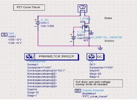
1. DC LOADLINE ANAYLSIS
DC simulation is used for finding the bias point and operating characteristics of the transistor. Below circuit shows characteristics for MOSFET.
Fig 3. FET Curve Tracer circuit in ADS
Fig 4. FET Curve Tracer simulation in ADS
2. BIAS AND STABILITY ANALYSIS
ISSN(Online): 2320-9801
ISSN (Print): 2320-9798
I
nternational
J
ournal of
I
nnovative
R
esearch in
C
omputer
and
C
ommunication
E
ngineering
(An ISO 3297: 2007 Certified Organization)
Vol. 3, Issue 6, June 2015
Fig 5. Bias and Stability circuit of FET in ADS
Fig 6. Bias and Stability circuit simulation of FET MRF134 in ADS
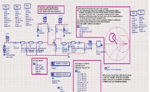
3. LOADPULL SIMULATION
Load pull simulation is utilized to find the optimal load value that will maximize the output power and the efficiency, or achieve a compromise between both of them. This analysis utilizes the built-in ADS load-pull circuit simulator. Different values of load impedance are applied to find out the optimum one, which meets the required value of gain, output power and efficiency. Before running the simulation, some parameters like frequency, V_high and V_low have to be set. The load pull circuit is shown below.
ISSN(Online): 2320-9801
ISSN (Print): 2320-9798
I
nternational
J
ournal of
I
nnovative
R
esearch in
C
omputer
and
C
ommunication
E
ngineering
(An ISO 3297: 2007 Certified Organization)
Vol. 3, Issue 6, June 2015
Fig 8. Load pull circuit simulation of FET MRF134 in ADS
4. HARMONIC BALANCE SIMULATION
To study the performance of the design regarding the output power and efficiency, one tone harmonic balance must be done. The Harmonic Balance circuit is shown below.
Fig 9. Harmonic Balance circuit of FET MRF134 in ADS
ISSN(Online): 2320-9801
ISSN (Print): 2320-9798
I
nternational
J
ournal of
I
nnovative
R
esearch in
C
omputer
and
C
ommunication
E
ngineering
(An ISO 3297: 2007 Certified Organization)
Vol. 3, Issue 6, June 2015
IX. CONCLUSIONS
This paper proposes design of Solid State Power Amplifier for radar applications using ADS software. Here we are designing a power amplifier by using MRF134 and performing DC simulation, S-parameters simulation, Loadpull simulation and Harmonic Balance simulation.
REFERENCES
[1] P. Saad, H. M. Nemati, M. Thorsell, K. Andersson, and C. Fager, "An opposite class-F GaN HEMT power amplier with 78% PAE at 3.5 GHz," in 39rd Eur. Microw. Conf., Oct. 2009, vol. 1, pp. 496-499
[2] A. Adahl and H. Zirath, "A 1 GHz class E LDMOS power amplier," in 33rd Eur. Microw. Conf., Oct. 2003, vol. 1, pp. 285– 288
[3] D. Kang, D. Kim, J. Choi, J. Kim, Y. Cho, and B. Kim, "A multimode/multiband power amplier with a helped suply modulator," IEEE Trans. Microw. Hypothesis Tech., vol. 58, no. 10, pp. 2598–2608, Oct. 2 010
[4] J. Kang, D. Yu, K. Min, and B. Kim, "A ultra-high PAE Doherty amplifier based 0.13-mm CMOS process," IEEE Microw. Remote Compon. Lett., vol. 16, no. 9, pp. 505–507, Sep.
[5] G. S. Cripps, “RF Power Amplifiers for Wireless Communications,”Artech House, 1999, chapters 3, 5, 8. [6] Harald, Par Rundqvist, “Active Microwave Circuit”, Chalmers University.
[7] “The Design of CMOS Radio-Frequency Integrated Circuits”, second edition, ByThomas H. Lee.
BIOGRAPHY
G. Anusha passed B.Tech (E.C.E) at G. Narayanamma Institute of Technology and Science, Hyderabad, in 2013 and pursuing M.Tech (DECS) at Sri PadmavathiMahilaViswavidyalyam.
A. SaiSuneel, passed B.Tech. (E.C.E) at Kuppam Engineering College, Kuppam and M.Tech. (Digital Electronics and Communication Systems), Tirupati. He published 14 International Journals and 1 National Journal. He is participated in 10 National Conferences, International Conferences and 3 Workshops.