ISSN(Online): 2320-9801
ISSN (Print): 2320-9798
International Journal of Innovative Research in Computer
and Communication Engineering
(An ISO 3297: 2007 Certified Organization)
Vol. 3, Issue 2, February 2015
Design of a Programmable Low Drop-Out
Regulator using CMOS Technology
Anjali V. Nimkar
1, Shirish V. Pattalwar
2, Preeti R. Lawhale
3M.E Student, Department of Electronics and Telecommunication, Prof. Ram Meghe Institute of Technology &
Research, Amravati, M.S, India 1
Associate Professor, Department of Electronics and Telecommunication, Prof. Ram Meghe Institute of Technology &
Research, Amravati, M.S, India 2
Assistant Professor, Department of Electronics and Telecommunication, Prof. Ram Meghe Institute of Technology &
Research, Amravati, M.S, India 3
ABSTRACT: Low drop-out regulators (LDO) are circuits which are designed to provide a stable and specified DC voltage, with a low input-to-output voltage difference. To get a new approach of power management towards a design of a low drop-out voltage regulator that provides a modern system on chip (SoC) solution and fulfils the present commercial requirements as well as the upcoming demands of the future, it becomes necessary to design the LDO regulator which gives all-rounder performance. This LDO should beware of various performance matrices. Also future nm technology offers more advantages in achieving most of the performance specifications. This paper presents a low-voltage low-dropout regulator that is capable of providing regulated output with small drop-out low-voltage and offers a range of different voltages, by using two binary-input control signals. The entire circuit has been designed in a 32 nm technology and simulated using Microwind tool. This design utilizes a cascode current amplifier used with a high threshold PMOS operated in the sub-threshold region, which is responsible to boost the gain and yield the desired output voltage.
KEYWORDS:Low Drop-Out, Low Power, 32nm, CMOS technology.
I. INTRODUCTION
CMOS linear regulators are widely used in battery-powered portable electronics devices as their low drop-out and low supply current characteristics found more advantageous in the world of electronics. The dropout voltage of a regulator is defined as that value of differential voltage at which regulation provided by the control loop stops. The regulator is a device that adjusts a voltage divider network to maintain a constant output voltage, and continually dissipates the difference between the input and regulated voltages as waste heat. The low drop-out nature of the regulator makes it appropriate for use in many applications namely automotive, portable, industrial, and medical applications. LDO regulators enable battery to be used up to the certain limit, and therefore the regulators are now essential power management ICs for the devices like mobile phones, digital cameras, and laptop PCs to have long battery life. Also Low quiescent current flow is important in portable products where the total current drain determines battery life.
ISSN(Online): 2320-9801
ISSN (Print): 2320-9798
International Journal of Innovative Research in Computer
and Communication Engineering
(An ISO 3297: 2007 Certified Organization)
Vol. 3, Issue 2, February 2015
Main focus is to design a programmable low-dropout (LDO) voltage regulator that can operate with a very small input output differential voltage with 32nm CMOS technology whose output voltage level is controlled externally by means of control signals. The operation of the LDO circuit is based on feeding back an amplified error signal to control the output current flow of the power transistor driving the load. More emphasis is given on the compactness and regulator is proposed to combat with stability and regulation issues. Integrating the power management circuit into system on-a-chip (SoC) devices has become a growing trend in SoC development [3].Proposed design is a complete SOC(system on chip) design which provides many circuit applications in portable, industrial and medical sectors.
II. RELATEDWORK
From review of published literature, it is observed that many researchers have designed different models of low drop-out regulator by applying different methodologies. Also many phenomena have been undertaken to enhance the transient response of the LDO regulators and to combat with stability issues and power management problems. It is seen that nm technology proves better in achieving required performance specifications. An error amplifier structure to improve load regulation of low voltage, low-dropout regulators can be employed. In [5]–[7], external control signals open or short the switch transistors to change the feedback resistor divider ratio to achieve a programmable output voltage. A LDO regulator using a simple OTA-type EA plus an adaptive transient accelerator achieve fast transient response, low IQ, and high PSR under a wide range of operating conditions [1]. By comparing circuit topologies for designing LDO regulator, it is seen that in general, all LDO specifications constrain each other. It is difficult to improve all of them simultaneously. The capacitor less LDO architecture overcomes the typical load transient and ac stability issues [4]. Furthermore, the designing can be possible with digital implementation [2] and programmability can be added to increase application area. As future nm technology offers more advantages in achieving most of the performance specifications so it is beneficial to propose the regulator with the selection of lower order of nm technology to fulfil targeted demands.
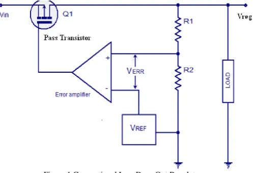
III.CONVENTIONALLOWDROP-OUTVOLTAGEREGULATOR
A low-dropout linear regulator will operate with input voltages only slightly higher than the desired output voltage. Figure 1 shows conventional low drop-out regulator. A voltage reference is used with the op-amp to generate a regulated voltage; it provides a constant output voltage which will be compared with the output voltage from the feedback network. If the voltage reference is stable with temperature, the fact that the Vreg is a function of a ratio of resistors and the variation in the op-amp’s open loop gain is desensitized using feedback makes the regulated voltage stable with process and changes in temperature.
.
Figure 1.Conventional Low Drop-Out Regulator
ISSN(Online): 2320-9801
ISSN (Print): 2320-9798
International Journal of Innovative Research in Computer
and Communication Engineering
(An ISO 3297: 2007 Certified Organization)
Vol. 3, Issue 2, February 2015
transistor. This device must be very wide so that it can source large load currents with a reasonable gate-source voltage. The length remains at the minimum value to keep the threshold voltage low. The output voltage of the LDO is at the drain of PMOS pass transistor, and resistors R1 and R2 form a voltage divider to feed a fraction of the output voltage back to the input. R1 and R2 are made large so that very little current flows through them, minimizing the power consumption of the feedback path. The loop gain depends on the products of the voltage gains of the two main gain stages in system architecture. The high loop gain provides good line and load regulations.
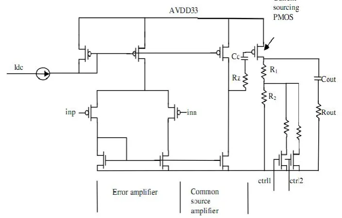
IV.PROPOSEDREGULATORARCHITECTURE ANDITSWORKING
The error amplifier is capable of desensitizing variations in the gain of PMOS and NMOS device because of high gain and resistive feedback network. So that a stable regulated voltage output is obtained. Designs using a BJT for the pass element responsible for large increase in ground current as output load increases. MOSFET based LDOs are more energy efficient as the ground current increase with load is minimal. In proposed architecture, a current-sourcing PMOS in the output stage is added. It is required that the PMOS be pulled to ground so as to be biased into saturation region. Because of this, the existing topology is modified and a Common- Source Stage is added, with the amplifying device. This amplifying device used is large enough so as it is to be used as a strong pull down device. The Common-Source stage is responsible to enhance signal swing and boost the gain at the op-amp output, subsequently. The Common-Source stage also useful to pull the gate of the large PMOS low enough so that its gate-to-source voltage increases. If the feedback voltage is smaller than the reference voltage, the gate of the PMOS device is pulled to lower, so that more current is allowed to pass and increases the output voltage. If the feedback voltage is greater than the reference voltage, the gate of the PMOS device is pulled to higher, so that less current is allowed to pass and decreases the output voltage.
Programmability is added to the LDO by using two external control signals, ctrl1and ctrl2 which are applied at the gate inputs of two NMOS devices. The binary input brings that resistance into the circuit and controls the output voltage by biasing the transistor in saturation. The proposed architecture consists of the following stages:
Figure 2.Schematic of proposed regulator
A. Error Amplifier
ISSN(Online): 2320-9801
ISSN (Print): 2320-9798
International Journal of Innovative Research in Computer
and Communication Engineering
(An ISO 3297: 2007 Certified Organization)
Vol. 3, Issue 2, February 2015
current source, along with the gate-drain connected load being driven by an ideal current source Idc. A current mirror NMOS load is responsible to provide high output impedance and high gain. An operational amplifier connected with this sort of load is termed as an open-transconductance amplifier, where all nodes are low impedance nodes with the exception of the differential pair [11].The resistive feedback network balances the amplifier by minimizing op-amp offset. The design of the output stage of the error amplifier has a substantial impact on the required size of the power transistor for the improvement of load regulation, especially when the supply voltage of the VLSI systems is low [3].
B .Common-Source Amplifier
In general, a source follower is used as the buffer stage in most LDO’s. The source follower is a simple implementation of the buffer which uses natural NMOS transistor and it has asymmetric current driving capability and limited gain. Hence a common-source amplifier is used. It has a small signal gain given
by-Av=gm (Ro1|| Ro2)
Here, gm is the transconductance of the amplifying device; Ro1 and Ro2 are the output resistances of the load and the amplifying device. When the amplifying device (NMOS) is made large enough, then we can get improved gain at the second stage. NMOS also acts as a strong pull down device, yielding rail-to-rail swing. Operational amplifiers with rail-to-rail output stage achieve the maximum output signal swing in systems with low single-supply voltages. They are capable of generating an output signal up to the supply rails.
C. Current-Sourcing PMOS
In our design, a PMOS with high voltage threshold has been used. If a lower voltage threshold PMOS is used, then we can get advantage of lesser area but low-voltage threshold FETs are known to contribute to leakage currents, increasing power dissipation in the device. Therefore current-sourcing is used which is responsible for quick charging and discharging of the output node, capable of increasing slew rate to obtain faster settling times.
V. IMPLEMENTATIONUSING32NMCMOSTECHNOLOGY
The proposed LDO is designed using 32 nm CMOS/VLSI technology in MICROWIND 3.1. The effective gate length required for this technology is 28nm. The main novelties related to the 32nm technology are high-k gate oxide, metal gate, 3rd generation high-k channel strain and very low-k interconnect dielectric. These key features of 32 nm technologies are provided from various providers like TSMC, Fujitsu, Intel, etc. As compared to 45nm CMOS technology, 32nm CMOS technology offers:
30% increase in switching performance. 30 % reduction in Power consumption 2 times higher density.
2 times reduction of the leakage between source and drain and through the gate oxide.
ISSN(Online): 2320-9801
ISSN (Print): 2320-9798
International Journal of Innovative Research in Computer
and Communication Engineering
(An ISO 3297: 2007 Certified Organization)
Vol. 3, Issue 2, February 2015
Figure 3.CMOS layout of LDO regulator
The MICROWIND3.1 program allows designing and simulating an integrated circuit at physical description level. The package consists of library of common logic and analog ICs to view and simulate. Also this program includes all the commands for a mask editor as well as original tools never gathered before in a single module (2D and 3D process view, VERILOG compiler, tutorial on MOS devices). Every step of design follows the design flow of MICROWIND 3.1 software. The design methodology will be according to VLSI backend design flow. Fig shows CMOS layout of proposed structure. The main objective is to design and analysis of the low drop-out regulator. We can gain access to circuit simulation by pressing one single key. The electric extraction of circuit is automatically performed and the analog simulator produces voltage and current curves immediately.
.
Figure 4.CMOS design Flow
VI.RESULTANDDISCUSSION
ISSN(Online): 2320-9801
ISSN (Print): 2320-9798
International Journal of Innovative Research in Computer
and Communication Engineering
(An ISO 3297: 2007 Certified Organization)
Vol. 3, Issue 2, February 2015
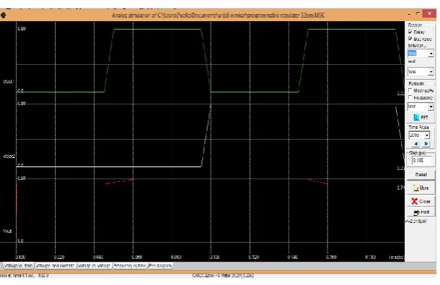
Figure 5.Regulated output voltage waveform
This programmability allows two different output voltages for four control inputs with dropout voltage of only 60 mV. Power consumption is very low as it consumes 2.019µw of power. More than one application can make use of programmability.
Binary input Output voltage
00 0.74
01 0.80
10 0.80
11 0.74
Table.1 Range of output voltages
Reduction of VDD emerges as a very effective means of limiting the power consumption. For the proposed LDO, power supply VDD of 0.80 volt is applied. The width of proposed LDO is 5.7µm & its height is 2.7µm.Thus the surface area of proposed Programmable LDO is 15.2µm2.The total number of NMOS devices used are 5 & PMOS devices are 6.The electrical nodes used are 20.
VII. CONCLUSION
ISSN(Online): 2320-9801
ISSN (Print): 2320-9798
International Journal of Innovative Research in Computer
and Communication Engineering
(An ISO 3297: 2007 Certified Organization)
Vol. 3, Issue 2, February 2015
Following table shows the parameters of proposed LDO after the simulation process targeted in microwind3.1
Foundry used 32nm CMOS technology
Vdd/Vout 0.8/
Programmable Vout 00/11-0.8
01 /10-0.74
Number of NMOS 5
Number of PMOS 6
Power consumption 2.019µw
Temperature 270 C
Surface area 15.2µm2
Drop-out voltage 60mV
Table2. Parameters of programmable LDO regulator
The design yields about 30 dB gain, but better gain can be achieved by further increase in transconductance of the differential pair. Also by reducing the number of stages and using cascade topology with resistive biasing can generate greater gain. In this architecture, the external capacitor used is quite large of 1pF, but capacitorless architectures [4] have been proposed and form a significant part of current CMOS LDO design literature. The current design hence has scope of improvement in this direction. The large external capacitor used in typical LDOs can be removed allowing for greater power system integration for system-on-chip (SoC) applications that require a sound compensation scheme for both the transient response and the alternating current (ac) stability. Furthermore, the designing can be possible with digital implementation and programmability can be added to become suitable for more applications considering the advancement of future technology.
REFERENCES
1. Chung-Hsun Huang,Ying-Ting Ma, and Wei-Chen Liao, “Design of a Low-Voltage Low-Dropout Regulator,” IEEE Transactions on Very Large
scale Integration (VLSI) systems, vol. 22, no. 6, pp.1308-1313,June 2014.
2.Yen-Chia Chu and Le-Ren Chang-Chien, “ Digitally Controlled Low-Dropout Regulator with Fast-Transient and Autotuning Algorithms’’ IEEE
Transactions on Power Electronics, vol. 28, no. 9,pp.4308-17, September 2013.
3. Ka Nang Leung, Yuan Yen Mai, and Philip K. T. Mok “ A Chip-Area Efficient Voltage Regulator for VLSI Systems’’, IEEE Transactions on
Very Large Scale Integration (VLSI) systems, vol. 18, no. 12,pp.1757-62, December 2010.
4. R. J. Milliken, J. Silva-Martinez, and E. Sanchez-Sinencio, “Full on-chip CMOS Low-Dropout Voltage Regulator,”IEEE Trans. Circuits Syst. I,
Reg. Papers, vol. 54, no. 9, pp. 1879–1890, Sep. 2007.
5. Y. C. Wu, C. Y. Huang, and B. D. Liu, “A Low Dropout Regulator with Programmable Output,” in Proc. IEEE Conf. Ind. Electron. Appl., pp. 3357–3361, June 2009.
6. J. M. Shen, W. B. Yang. Y. Huieh, and Y. L. Lo, “A Low Power Multi-Voltage Control Technique with Fast-Settling Mechanism for Low Dropout Regulator,” in Proc. IEEE Int. Symp. Integr. Circuits pp. 558–561, Feb 2009.
7. C. Y. Tseng, L. W. Wang, and P. C. Huang, “An integrated linear regulator with fast output voltage transition for dual-supply SRAMs in DVF system,” IEEE J. Solid-State Circuits, vol. 45, no. 11, pp. 2239–2249,Nov. 2010.
8. G. Patounakis, Y. W. Li, and K. Shepard, “A fully integrated on-chip DC-DC conversion and management system’’,IEEE J. Solid-State Circuits, vol. 39, no. 3, pp. 443–451, Mar. 2004.
9. Gabriel A. Rincon-Mora, and Phillip E. Allen, Fellow, “A Low-Voltage, Low Quiescent Current, Low Drop-Out Regulator” IEEE Journal of
Solid-state Circuits, vol. 33, no.1, pp.36-44, January 1998
10. “An Improved CMOS Error Amplifier Design for LDO Regulators in Communication Applications” by Xinquan Lai, Institute of Electronic CAD and Donglai Xu, School of Science and Technology