Available online: https://edupediapublications.org/journals/index.php/IJR/ P a g e | 4597
A BSTRACT: Redu n d an t Bas ed M u ltip lier Ov er Gau lo is Field (GF(2m)) has gained more po p u larity in elliptic curve cryptography (ECC) main ly d u e to th eir negligib le h ard ware co s t fo r s q u arin g an d mo d ular reduction. In this paper, we have proposed a n o vel recursive d eco mp o s itio n alg o rith m fo r RB mu ltiplication to obtain high throughput d ig it -s erial imp lementation. Depends up on a specific featu re o f red undant representation in a clas s o f fin ite field s , two new multiplication algorithms alo n g with th eir p ertaining architectures are proposed to alleviate this p ro b lem. Co n s id er an area-d elay p ro d u ct as a measure o f evaluation, it has been sho wn th at b o th th e proposed architectures considerably o u tp erfo rm exis ting digit-level multipliers by utilizing th e s ame b asis. It is also shown that for a subset of th e field s , th e proposed multipliers are of higher performance in terms of area-d elay co mp lexities amo n g s ev eral recently proposed optimal normal basis mu ltip liers . Th e main characteristics of the p o s t p lace & ro u te ap plication specific integrated circuit imp lementation o f the proposed multipliers for three p ractical d ig it s izes are als o rep o rted .
In d ex Terms: Digit-level arch itectu re, fin ite field arithmetic, mu ltip licatio n alg o rith m, red u n d an t rep res en tatio n .
I.INTRODUCTION
Finite field computation has gained growing attention because of its wide range of applications in coding theory, error control coding, and especially in cryptography, where ElGamal and elliptic curve cryptography (ECC) two out of the three well-known cryptosystems, are depends on
finite field arithmetic. Finite field computation is performed by utilizing arithmetic operations in the underlying finite field. Among the basic field operations, multiplication plays a fundamental role as more complicated operations, namely, field exponentiation and field inversion can be carried out with consecutive use of field multiplication.
Similar to linear algebra, the concept of representation bases is also used in finite field arithmetic to represent field elements. The choice of representation system mainly affected by the hardware in use and the requirements of the cryptosystem, has a great impact on computational performance.
A few number of representation systems for extension binary fields have been proposed in the literature, such as polynomial basis normal basis (NB), redundant basis (RB), and dual basis. In both normal basis (NB) and redundant representation (RB), squaring operation can be performed by applying a simple permutation operation on the coordinates. Moreover, redundant representation is of a special interest because of its unique feature in accommodating ring type operations. This not only offers almost
Design An High Speed Bypass Multiplier For Communication
1GUNTUPALLI. MANISRI, 2CHALLAGUNDLA. PAPA RAO
1M.tech-Scholar, Dept of ECE, Guntur Engineering College, Guntur, A.P, India
Available online: https://edupediapublications.org/journals/index.php/IJR/ P a g e | 4598 cost-free squaring operation but also
eliminates the need for modular reduction in multiplication.
II.EXISTED SYSTEM
Fig. 1 shows the architecture, hereafter referred to as digit-level symmetrical Redundant Basis RB type−a multiplier. From top to bottom, the architecture contains an n-bit circular shift register which should be initialized with the coordinates of operand B. This shift register provides inputs to a wire expansion module with n inputs and w(n − 1) outputs followed by ((n − 1)/2) identical modules shown inside the dashed boxes.
FIG. 1.EXISTED A RCHITECTURE FOR DIGIT -LEVEL SIPO RB M ULTIPLIER
At the bottom, there is a network of XOR gates adding 2w outputs of each module together to form output coordinates. Each module is made of a layer of 2w AND gates receiving the outputs of the wire expansion module as their first input set. The second input set is received from certain bits of operand A in a digit-serial fashion. Each
AND gate is followed by an XOR gate connected immediately to a flip-flop.
The output of the flip-flop is fed back to the XOR gate forming an accumulation unit together. Two AND gates along with their respective accumulation units form a structure responsible to realize the operations. One of these structures is shown in the Fig. 1 inside a dotted block for j = 0 and k = 0. In total, the architecture contains w(n − 1/2) such structures, each of which consists of two AND gates, two XOR gates, and two flip-flops to generate and store each clock cycle.
III.PROPOSED ARCHITECTURE
FIG 2.PROPOSED A RCHITECTURE
Available online: https://edupediapublications.org/journals/index.php/IJR/ P a g e | 4599 two cycles to complete in the proposed
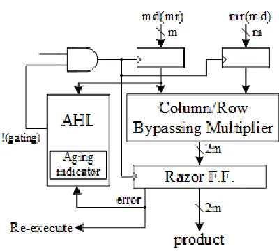
architecture the column- and row-bypassing multipliers can be examined by the number of zeros to predict in either the multiplicand or multiplicator. The number of ones and zeros in the multiplicand and multiplicator follows a normal distribution when input patterns are random.
Hence, By using similar architecture, the difference between the two bypassing multipliers lies in the input signals of the AHL and the two aging-aware multipliers can be implemented. According to the bypassing selection in the column or row-bypassing multiplier, the architecture with the column-bypassing multiplier the input signal of the AHL is the multiplicand, whereas that of the row-bypassing multiplier is the multiplicator. By utilizing Razor flip-flops timing violations occur before the next input pattern arrives can be detected.
FIG 3. RA ZOR FLIP-FLOPS
A 1-bit Razor flip-flop consists of a main flip-flop, shadow latch, XOR gate, and mux. The shadow latch catches the execution result using a delayed clock signal, which is slower than the normal clock signal and the main flip-flop catches the execution result for the combination circuit using a normal clock signal. The path delay of the current
operation exceeds the cycle period, and the main flip-flop catches an incorrect result if the latched bit of the shadow latch is different from that of the main flip-flop. To notify the system the Razor flip-flop will set the error signal to 1 to re execute the operation if any errors occur and notify the AHL circuit that an error has occurred. To detect whether an operation is considered to be a one-cycle pattern can really finish in a cycle we utilize Razor flip-flops. If not, the operation is reexecuted with two cycles. Although the reexecution may seem costly, because of the reexecution frequency is low then overall cost is low.
FIG 4. DIA GRA M OF A HL
Available online: https://edupediapublications.org/journals/index.php/IJR/ P a g e | 4600 The column-or row-bypassing multiplier is
not able to complete these operations successfully, if the cycle period is too short causing timing violations. These timing violations will generate error signals which be caught by the Razor flip-flops. If errors happen frequently and exceed a predefined threshold, it means the circuit has suffered significant timing degradation due to the aging effect and the aging indicator will output signal 1; otherwise, it will output 0 to indicate the aging effect is still not significant, and no actions are needed.
In the AHL circuit first judging block will output 1 If the number of zeros in the multiplicand is larger than n. The second judging block in the AHL circuit will output 1 if the number of zeros in the multiplicand (multiplicator) is larger than n + 1. Whether an input pattern requires one or two cycles, they are both employed to decide but only one of them will be chosen at a time. The aging effect is not significant, and the aging indicator produces 0, in the beginning, so the first judging block is used. When the aging effect becomes significant, after a period of time the second judging block is chosen. The second judging block allows a smaller number of patterns to become one-cycle patterns when compared with the first judging block, because it requires more zeros in the multiplicand (multiplicator).
The operation details of the AHL circuit are as follows: whether the pattern requires one cycle or two cycles to complete when an input pattern arrives and pass both results to the multiplexer will decided by both judging blocks. Based on the output of the aging
indicator the multiplexer selects one of either result. Then between the result of the multiplexer, an OR operation is performed and the .Q signal is used to determine the input of the D flip-flop. The output of the multiplexer is 1 when the pattern requires one cycle,. The !(gating) signal will become 1, and in the next cycle the input flip flops will latch new data. On the other hand, when the output of the multiplexer is 0, which means the input pattern requires two cycles to complete, the OR gate will output 0 to the D flip-flop. Therefore, the !(gating) signal will be 0 to disable the clock signal of the input flip-flops in the next cycle. Note that only a cycle of the input flip-flop will be disabled because the D flip-flop will latch 1 in the next cycle.
Available online: https://edupediapublications.org/journals/index.php/IJR/ P a g e | 4601 IV. RESULTS
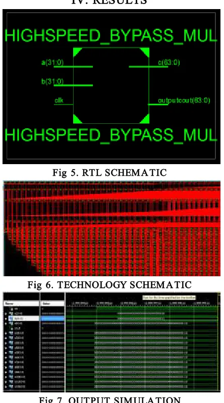
Fig 5. RTL SCHEM A TIC
Fig 6. TECHNOLOGY SCHEM A TIC
Fig 7. OUTPUT SIM ULA TION
V.CONCLUSION
This paper proposed an aging-aware variable latency multiplier design with the AHL. The multiplier is able to adjust the AHL to mitigate performance degradation due to increased delay. The proposed variable latency multipliers have less performance degradation due to the variable latency multipliers which have less timing waste, but traditional multipliers need to consider the degradation which is caused by both the BTI effect and electro-migration
and utilize the worst case delay as the cycle period.
VI.REFERENCES
[1] Y. Cao. (2013). Predictive Technology Model (PTM) and NBTI Model [Online]. Available: http://www.eas.asu.edu/∼ptm [2] S. Zafar et al., “A comparative study of NBTI and PBTI (charge trapping) in SiO2/HfO2 stacks with FUSI, TiN, Re gates,” in Proc. IEEE Symp. VLSI Technol. Dig. Tech. Papers, 2006, pp. 23–25.
[3] S. Zafar, A. Kumar, E. Gusev, and E. Cartier, “Threshold voltage instabilities in high-k gate dielectric stacks,” IEEE Trans. Device Mater. Rel., vol. 5, no. 1, pp. 45–64, Mar. 2005.
[4] H.-I. Yang, S.-C. Yang, W. Hwang, and C.-T. Chuang, “Impacts of NBTI/PBTI on timing control circuits and degradation tolerant design in nanoscale CMOS SRAM,” IEEE Trans. Circuit Syst., vol. 58, no. 6,pp. 1239–1251, Jun. 2011.
[5] R. Vattikonda, W. Wang, and Y. Cao, “Modeling and miimization of pMOS NBTI effect for robust naometer design,” in Proc. ACM/IEEE DAC, Jun. 2004, pp. 1047–1052
1GUNTUPALLI. MANISRI pursuing M.Tech
in Guntur Engineering College, Guntur. Her area of interest is VLSI.
2CHALLAGUNDLA. PAPA RAO passed his