Electromagnetic Waves Radiation by a Vibrators System
with Variable Surface Impedance
Sergey L. Berdnik, Victor A. Katrich, Mikhail V. Nesterenko*, and Yuriy M. Penkin
Abstract—The problem of electromagnetic waves radiation by a vibrators system with variable distributed surface impedance along their axes located in free space is solved by the generalized method of induced electromotive forces (EMF). The distinctive peculiarity of this method is the use of the functional distributions, obtained as a result of the analytical solution of the integral equation for the current by the asymptotic averaging method before, as the basic approximations for the currents along the impedance vibrators. The multi-parameter characteristics of three-element and multi-element antennas with variable impedance vibrators are calculated.
1. INTRODUCTION
Systems of perfectly conducting vibrators are widely used both as antennas with directional axial radiation and as a multi-element antenna array in the meter and decimeter wave bands [1–10]. An additional parameter, which allows forming a required amplitude-phase distribution of vibrators currents, and thus, modifying and optimizing the electromagnetic characteristics of the system as a whole, can be distributed surface impedance (both constant and variable along the vibrator length) [11– 16]. The length of impedance vibrators can be both shorter or longer than that of a perfectly conducting vibrator. This is particularly important when there exist restrictions on radiator dimensions. Here we present a mathematical model of the impedance vibrator systems in the free space, characterized by the surface impedances and by its distribution functions along the vibrators length.
2. FORMULATION OF THE PROBLEM AND SOLUTION OF INTEGRAL EQUATIONS FOR THE CURRENTS
Consider a system consisting ofN parallel impedance vibrators in the free space. Let 2Lnandrnbe the length and radius of the n-th vibrator, respectively. The vibrators centers in the Cartesian coordinate system are zn, xn, yn. The projection of electric fields E0sn(sn) of extraneous sources on the n-th vibrator axis (n= 1,2, . . . , N) can be decomposed into two parts relative to the geometric center of the vibrator: a symmetric E0ssn(sn) and anti-symmetricE0asn(sn) marked by the superscriptssand a. The variable sn is the local coordinate along the axis of the n-th vibrator. A system of integral equations relative to vibrators currentsJn(sn) can be written as follows [11]
N
n=1
d2 ds2
m+k
2
Ln
−Ln
Jn(sn)Gsm(sm, sn)dsn=−iω[E0sm(sm) +zim(sm)Jm(sm)], m= 1,2, . . . , N, (1)
Received 16 September 2016, Accepted 18 October 2016, Scheduled 3 November 2016
* Corresponding author: Mikhail V. Nesterenko ([email protected]).
where zim(sm) = rim+ixim(sm) is the internal complex impedance per unit length [Ohm/m] of the m-th vibrator, which may be variable along the vibrator length; k= 2π/λ,λis the wavelength in free space;ω is the circular frequency.
Since the fields of extraneous source are presented by two components, each vibrator current consists of two terms, symmetric and antisymmetric, i.e., Jn(sn) = Jns(sn) +Jna(sn). Let us now present the vibrator currents as a product of the unknown complex amplitudes and predefined scalar function fnqs,a(sn)(q= 0,1, . . . , Q) as
Jns,a(s) = Q
q=0
Jnqs,afnqs,a(sn), fnqs,a(±Ln) = 0. (2)
Then the system of Equation (1) can be written as
N n=1 Q q=0 d2 ds2 m +k2
Ln
−Ln
Jnqs fnqs (sn) +Jnqa fnqa (sn)
Gsm(sm, sn)dsn−iωzim(sm) Q
p=0
Jmqs fmqs (sm)+Jmqa fmqa (sm)
=−iω[Es0sm(sm) +Ea0sm(sm)]. (3)
Let us multiply, following the generalized method of induced EMF [11, 13], the left- and right-hand sides of Equation (3) by fmps (sm) and fmpa (sm) (p= 0,1, . . . , Q) and integrate results over the length of the vibrators. Thus, we arrive at the system of linear algebraic equations for the current amplitudes Jnqs and Jnqa
⎧ ⎪ ⎪ ⎪ ⎪ ⎪ ⎨ ⎪ ⎪ ⎪ ⎪ ⎪ ⎩ N n=1 Q q=0 Jnqs
Zmn,pqss +δmnZ˜m,pqss
+Jnqa
Zmn,pqsa +δmnZ˜m,pqsa
=−iω 2kE
s
0mp,
N n=1 Q q=0 Jnqs
Zmn,pqas +δmnZ˜m,pqas
+Jnqa
Zmn,pqaa +δmnZ˜m,pqaa
=−iω 2kE
a
0mp,
(4) where Z ⎧ ⎪ ⎨ ⎪ ⎩ ss aa sa as ⎫ ⎪ ⎬ ⎪ ⎭ mn,pq = 1
2k Lm
−Lm
f ⎧ ⎪ ⎨ ⎪ ⎩ s a s a ⎫ ⎪ ⎬ ⎪ ⎭ mp (sm)
⎡ ⎢ ⎢ ⎢ ⎢ ⎢ ⎣ d2 ds2
m +k
2
Ln
−Ln
f ⎧ ⎪ ⎨ ⎪ ⎩ s a a s ⎫ ⎪ ⎬ ⎪ ⎭
nq (sn)Gsm(sm, sn)dsn
⎤ ⎥ ⎥ ⎥ ⎥ ⎥ ⎦dsm,
˜ Z ⎧ ⎪ ⎨ ⎪ ⎩ ss aa sa as ⎫ ⎪ ⎬ ⎪ ⎭
m,pq = −iω
2k Lm
−Lm
f ⎧ ⎪ ⎨ ⎪ ⎩ s a s a ⎫ ⎪ ⎬ ⎪ ⎭ mp (sm)f
⎧ ⎪ ⎨ ⎪ ⎩ s a a s ⎫ ⎪ ⎬ ⎪ ⎭
mq (sm)zim(sm)dsm,
E0s,amp =
Lm
−Lm
fmps,aE0s,asm(sm)dsm, δmn=
1 if m=n, 0 if m=n .
As an example, let us consider the Yagi-Uda antenna [2–10] (Fig. 1).
Let the vibrators be arranged so that their central points are on the z-axis of the Cartesian coordinate system, and the longitudinal axes of the vibrators are oriented parallel to the x-axis. Let us enumerate the vibrators n = 1,2, . . . , N by their position on the z-axis, so that n = 1 and n = 2 correspond to the active vibrator and reflector, respectively, and the remaining vibrators are directors. The active vibrator (n = 1) is excited at its center (s1 = 0) by δ-generator of harmonic oscillations
with voltage amplitude V0. Thus, the projection of the electric field of extraneous sources on the
longitudinal axis of the active vibrator has only symmetric component E0s1(s1) = E0ss1(s1) =V0δ(s1)
Figure 1. The configuration of Yagi-Uda antenna.
the active vibrator by functions f10s(s1) = sin ˜k(L1− |s1|) and f11s (s1) = cos ˜ks1 −cos ˜kL1, while the
currents on the passive vibrators by functions fns1(sn) = cos ˜ksn−cos ˜kLn (n = 2,3, . . . , N). Here
˜
k=k−i2πzinav
Z0Ω ,zavin = 1 2Ln
Ln
−Ln
zin(sn)dsn is the mean internal impedance along the vibrator length [11],
Z0 = 120π Ohm and Ω = 2 ln(2Ln/rn). The current distribution functions were obtained as solutions of
the integral equation for the current on a solitary impedance vibrator by the averaging method [11, 12]. The impedance distribution along the vibrators can be represented by zin(sn) =zinavφn(sn), where the distribution functions φn(sn) are normalized so that mean values over the vibrator length were equal to unit. In general case, the normalized surface impedance of the vibrator ¯ZSn = 2πrnzin/Z0 can be
complex so that ¯ZSn = ¯RSn+iX¯Sn. If ¯XSn >0 the impedance is of inductive type and ¯XSn =krnCLn, and if ¯XSn < 0, the impedance is of capacitive type and ¯XSn = −CCn/(krn) where the constants CLn and CCn are defined by the vibrator dimensions and physical parameters of the vibrator material. Formulas defining specific realizations of the vibrator surface impedance are given in Appendix A.
The radiation pattern of Yagi-Uda antenna (Fig. 1) can be written as follows
F(θ, ϕ) = 1
Fm sin (arccos (sinθcosϕ)) N
n=1
⎡
⎣eikzncosθ
Ln
−Ln
Jn(sn)eiksnsinθcosϕdsn ⎤ ⎦,
where 1/Fm is the normalizing factor. The radiation patterns in E- and H-vector’s planes may be defined as FE =F(θ, ϕ= 0◦) and FH =F(θ, ϕ= 90◦), respectively.
3. NUMERICAL RESULTS
It is known that the characteristics of the Yagi-Uda antenna can be varied by adjusting the lengths of vibrators and distances between them. To obtain axial radiation of the Yagi-Uda antenna composed of perfectly conducting vibrators, the directors should be slightly shorter and the reflector should be longer than the active vibrator (Fig. 2(a)). Recent studies have shown that the reactance of the vibrators in the Yagi-Uda array required to obtain the necessary input parameters and radiation characteristics can also be achieved by variable the magnitude and distribution function of the surface impedance of the fixed length vibrator. The electrical length of the impedance vibrators can be both shorter and longer than that of the perfectly conducting vibrator.
(a) (b) (c)
Figure 2. Three-element Yagi-Uda antenna array: (a) perfectly conducting vibrators (2L1 = 0.44λ0,
2L2 = 0.5λ0, 2L3 = 0.38λ0); (b) inductive impedance vibrators (2Ln = 0.35λ0); (c) capacitive
impedance vibrators (2Ln= 0.65λ0).
-1.0 -0.5 0.0 0.5 1.0
0.0 0.5 1.0 1.5 2.0
D
is
tr
ib
u
ti
o
n
fu
n
cti
o
n
φn
(
sn
)
Relative coordinate sn/Ln director (β=2.1) reflector (β=1.7)
active vibrator
-1.0 -0.5 0.0 0.5 1.0
0.0 1.0 2.0 3.0 4.0 5.0
Relative coordinate sn/Ln
D
is
tr
ib
u
ti
o
n
fu
n
cti
o
n
φn
(
sn
)
director (β=5.3)
reflector (β=1.7)
active vibrator
(a) (b)
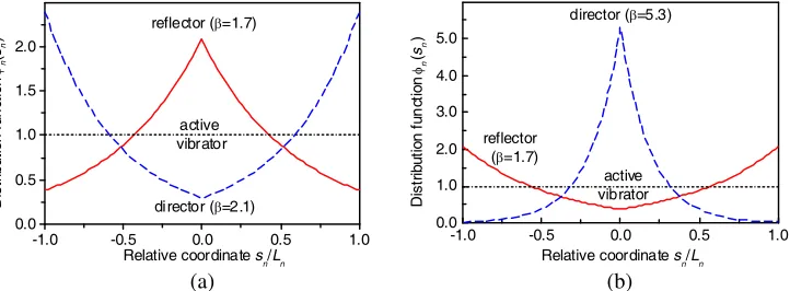
Figure 3. The distribution functions of the surface impedance of vibrators in Yagi-Uda arrays: (a) the inductive impedance; (b) the capacitive impedance (reflector, director, active vibrator).
relative to the impedance with CDF, while the inductive impedance with IDF and the capacitive impedance with DDF decrease the resonant length. That is, the DDF increases impedance while the IDF decreases it. This effect can be used during the design of antenna arrays. Let’s illustrate this possibility by numerical calculations of electrodynamic characteristics for a three-element Yagi-Uda antenna array with the equal-length vibrators and the variable inductive impedance ¯ZSn(sn) =iX¯Snavφn(sn) (Fig. 2(b)) and capacitive impedance ¯ZSn(sn) =−iX¯Snavφn(sn) (Fig. 2(c)). Since the normalized surface impedances
¯
XSnav of all vibrators in the array are equal, phases of currents in the radiators to ensure the axial radiation can be obtained by selection of the surface impedance distribution functions. The geometric parameters of array elements and impedances ¯XSnav should be selected so as to match the antenna input impedance at operating wavelength λ0 and the feeder line characteristic impedance and to provide a low voltage
standing-wave ratio (VSWR) in the feeder line of the active vibrator.
Consider the exponentially decreasing and exponentially increasing distribution functionsφn(sn) = αexp[−β|sn|/Ln] andφn(sn) =αexp[−β(|sn|/Ln−1)], whereα=β/[1−exp(−β)] is the normalization factor, andβis the arbitrary dimensionless constant. The functionsφn(sn) for the three antennas shown in Fig. 2 are plotted in Fig. 3.
The plots of VSWR in feeder lines with wave resistance W = 50 Ohm (curves 1, 4), W = 25 Ohm (curve 2), and W = 75 Ohm (curve 3) and directivity D versus the wavelength are shown in Fig. 4 for the three-element Yagi-Uda arrays (Fig. 2) with the impedance distribution presented in the Fig. 3 (CLnav = 1.448,CCnav = 5.466×10⁻³,rn= 0.01λ0,z2=−0.25λ0,z3= 0.2λ0).
As can be seen from the plots in Fig. 4(a), the antenna array with impedance vibrators and the feed line can be better matched than the antenna with perfectly conducting vibrators. Fig. 5 shows similar plots for seven-element arrays with perfectly conducting vibrators (2L1 = 0.45λ0, 2L2 = 0.5λ0,
0.90 0.95 1.00 1.05 1.10 1.15 1.0
1.5 2.0 2.5 3.0 3.5
VS
W
R
1 2 3 4
Relative wavelength λ/λ0
(a)
0.90 0.95 1.00 1.05 1.10 1.15
2.0 3.0 4.0 5.0 6.0 7.0 8.0
1 2 3 4
Di
re
c
tiv
e
g
a
in
D
Relative wavelength λ/λ0
(b)
Figure 4. VSWR and D versus the wavelength for the three-element Yagi-Uda antenna: curves 1, 4 — perfectly conducting vibrators, curve 4 was obtained by the method of moments with piecewise constant basis vibrators; curve 2 — vibrators with variable impedance of inductive type; curve 3 — vibrators with variable capacitive impedance.
0.90 0.95 1.00 1.05 1.10 1.15
1.0 1.5 2.0 2.5 3.0 3.5
1 2 3
VSW
R
Relative wavelength λ/λ0
(a)
0.90 0.95 1.00 1.05 1.10 1.15 2.0
4.0 6.0 8.0 10.0 12.0 14.0 16.0
1 2 3
Directive gain
D
Relative wavelength λ/λ0
(b)
Figure 5. VSWR and D versus the wavelength for the seven-element Yagi-Uda antenna: curve 1 — perfectly conducting vibrators, curve 2 — vibrators with variable impedance of inductive type; curve 3 — vibrators with variable capacitive impedance.
θo
(a) (b)
0.0 0.2 0.4 0.6 0.8 1.0
1 2 3
0.0 0.2 0.4 0.6 0.8 1.0
1 2 3
0 30 60 90 120 150 180
θo
0 30 60 90 120 150 180
|F H|
E
|F |
|F H|
E
|F |
H
E
|
F
|, |
F
|
H
E
|
F
|, |
F
|
Figure 6. The radiation patterns of the (a) three-element and (b) seven-element Yagi-Uda antennas: curves 1 — perfectly conducting vibrators, curves 2 — vibrators with variable impedance of inductive type; curves 3 — vibrators with variable capacitive impedance.
2Ln= 0.35λ0,CLnav = 1.464, β= 1.7 for the reflector and directors, W = 25 Ohm), and with impedance
vibrators (variable impedance of capacitive type: 2Ln = 0.65λ0, CCnav = 5.341×10⁻³, β = 1.7 for the
reflector andβ = 4.5 for the directors,W = 75 Ohm). The other parameters are as follows: rn= 0.01λ0,
As can be seen from the plots in Fig. 4(a) and Fig. 5(a), the array with the impedance vibrators is better matched with feed line than perfectly conducting vibrators. The inductive impedance decreases and capacitive impedance increases the array operating band defined using VSWR (for example, at the level VSWR = 2) and the directivity D as compared with the case ¯ZSn= 0.
The radiation patterns of the Yagi-Uda antennas atλ=λ0 are shown in Fig. 6.
4. CONCLUSION
The problem solution presented in the paper can be used as a basis for multi-parameter optimization of electrodynamic characteristics of radiating multi-element structures built on vibrators with variable distributed surface impedance. The distinctive peculiarity of the method, proposed by the authors, is the use of the approximating functions, resulting from the integral equation solution for the current by the asymptotic averaging method, in the current distribution along the impedance vibrator. The ground of rightness and correctness of such an approach is represented in the format of comparative analysis with the calculated results by the method of moments. One would note that the new conception of the generalized method of induced EMF, keeping all known advantages of numerical-analytical methods in comparison with direct numerical methods, extends to the cases of the vibrator with the impedance, variable along its length, and the impedance vibrators systems rather simply. Thus the proposed generalized method of induced EMF allows to widen the boundaries of numerical-analytical investigations of practically significant problems of the impedance vibrators application sufficiently.
APPENDIX A. SURFACE IMPEDANCE OF VIBRATORS
Formulas determining the distributed surface impedance of electrically thin vibrators (material parameters are: permittivityε, permeabilityμ, and conductivity σ) have the following form
No The vibrator design Vibrator model Impedance
1 Solid metal cylinder. The radius
satisfy inequality r >> Δ , Δ is
skin layer thickness.
0 1
120πσΔ S
i
Z = +
2 Metallized dielectric cylinder. Metal
layer thickness is h << Δ .
3 Metal-dielectric cylinder. 1 L is the
thickness of a metal discs, L2 is the thickness of a dielectric disks.
4 Magnetodielectric metalized cylinder. ri is the radius of internal conducting cylinder.
5 Metal cylinder coated with
magnetodielectric layer, which thickness is r − ri, or corrugated
cylinder ( )<<λ, where L1 is
crests thickness where , L2
is the notch width where .
6 Metal monofilar helix. r is helix
radius kr<<1, ψ is winding angle.
0 0
0 R
S
Z = 1
120πσh + ikrR (ε − 1)/2
2 i
krε +
S
Z = − L2
2 L 1 L
1
i
S
Z =
120πσh − i/krμ R ln(r/r )
+L2 1
L
S Z = 0
S
Z = 0/
S
Z = i/krμ ln(r/r i)
S
Z (s)= Z Sφ(s)
S
Formulas for surface impedances of vibrators are derived in the frame of the impedance concept [11] and valid for thin cylinders |(k√εμr)2ln(k√εμr
i)| 1 both for finite and infinite cylinders, located in the hollow electrodynamic volume. If vibrators are in a material medium with parameters ε1 and μ1,
all above formulas must contain the factor μ1/ε1.
REFERENCES
1. King, R. W. P., R. B. Mack, and S. S. Sandler,Arrays of Cylindrical Dipoles, Cambridge University Press, New York, USA, 1968.
2. Yagi, H. and S. Uda, “Projector of the sharpest beam of electric waves,” Proc. Imperial Academy
Japan, Vol. 2, 49–52, 1926.
3. Altshuler, E. E., “A monopole array driven from a rectangular waveguide,” IRE Trans. Antennas
and Propag., Vol. 10, 558–560, 1962.
4. Jones, E. A. and W. T. Joines, “Design of Yagi-Uda antennas using genetic algorithms,” IEEE
Trans. Antennas and Propag., Vol. 45, 1386–1392, 1997.
5. Sun, B.-H., S.-G. Zhou, Y.-F. Wei, and Q.-Z. Liu, “Modified two-element Yagi-Uda antenna with tunable beams,”Progress In Electromagnetics Research, Vol. 100, 175–187, 2010.
6. Formato, R. A., “Improving bandwidth of Yagi-Uda arrays,”Wireless Engineering and Technology, Vol. 3, 18–24, 2012.
7. Yeo, J., J.-I. Lee, and J.-T. Park, “Broadband series-fed dipole pair antenna with parasitic strip pair director,”Progress In Electromagnetics Research C, Vol. 45, 1–13, 2013.
8. Liu, H., S. Gao, and T.-H. Loh, “Small director array for low-profile smart antennas achieving higher gain,”IEEE Trans. Antennas and Propag., Vol. 61, 162–168, 2013.
9. Wang, Z., X. L. Liu, Y.-Z. Yin, J. H. Wang, and Z. Li, “A novel design of folded dipole for broadband printed Yagi-Uda antenna,” Progress In Electromagnetics Research C, Vol. 46, 23–30, 2014.
10. Zhang, Z., X.-Y. Cao, J. Gao, S.-J. Li, and X. Liu, “Compact microstrip magnetic Yagi antenna and array with vertical polarization based on substrate integrated waveguide,” Progress In
Electromagnetics Research C, Vol. 59, 135–141, 2015.
11. Nesterenko, M. V., V. A. Katrich, Yu. M. Penkin, V. M. Dakhov, and S. L. Berdnik,Thin Impedance
Vibrators. Theory and Applications, Springer Science+Business Media, New York, 2011.
12. Nesterenko, M. V., “Analytical methods in the theory of thin impedance vibrators,” Progress In
Electromagnetics Research B, Vol. 21, 299–328, 2010.
13. Nesterenko, M. V., V. A. Katrich, S. L. Berdnik, Y. M. Penkin, and V. M. Dakhov, “Application of the generalized method of induced EMF for investigation of characteristics of thin impedance vibrators,”Progress In Electromagnetics Research B, Vol. 26, 149–178, 2010.
14. Penkin, D. Y., V. A. Katrich, Y. M. Penkin, M. V. Nesterenko, V. M. Dakhov, and S. L. Berdnik, “Electrodynamic characteristics of a radial impedance vibrator on a conduction sphere,”Progress
In Electromagnetics Research B, Vol. 62, 137–151, 2015.
15. Yeliseyeva, N. P., S. L. Berdnik, V. A. Katrich, and M. V. Nesterenko, “Electrodynamic characteristics of horizontal impedance vibrator located over a finite-dimensional perfectly conducting screen,” Progress In Electromagnetics Research B, Vol. 63, 275–288, 2015.