An Improved MoM-GEC Method for Fast and Accurate
Computation of Transmission Planar Structures in Waveguides:
Application to Planar Microstrip Lines
Nejla Oueslati* and Taoufik Aguili
Abstract—This paper presents a new hybridization between MoM-GEC and a MultiResolution analysis (MR) based on the use of wavelets functions as trial functions. The proposed approach is developed to speed up convergence, alleviate calculation and then provide a considerable gain in requirements (processing time and memory storage) because it generates a sparse linear system. The approach consists in calculating the total current and input impedance on an invariant metallic pattern through two steps. The first one consists in expressing the boundary conditions of the unknown electromagnetic current with a single electrical circuit using the Generalized Equivalent Circuit method (GEC) and then deduce an electromagnetic equation based on the impedance operator [6, 7]. The impedance operator used here is described using the local modal basis of the waveguide enclosing the studied structure. The second step consists in approximating the total current using orthonormal periodic wavelets as testing functions and the local modal basis of the waveguide as basis functions. The proposed approach allows fast calculation of such inner products through the use of the wavelets multiresolution (MR) analysis advantages, thus significantly reducing the required CPU-time for microstrip-type structure analysis [13, 14]. A sparse matrix is generated from the application of a threshold. A sparsely filled matrix is easier to store and invert [15, 16]. Based on this approach, we study the planar structures. The obtained results show good accuracy with the method of moments. Moreover, we prove considerable improvements in CPU time and memory storage achieved by the MR-GEC approach when studying these structures.
1. INTRODUCTION
Microwave devices applications cover a wide band of electromagnetic domain and have numerous functions and dimensions according to their frequency range of use. To model such devices and their interactions, there is a set of methods that solves a number of problems, in some scope. Maxwell’s equations cannot be analytically solved in most cases. Hence, many modeling methods and various techniques have been developed to solve electromagnetic problems in time or frequency domain. They provide an approximate solution by numerically solving Maxwell’s equations, in differential or integral form.
Among all these numerical techniques, full wave ones [1, 2] have the most high return, since it is possible to know the electromagnetic field in any point by taking into account of singularities. All the publications in this domain [2, 3] have shown that the integral formulation was the best to set this method more efficiently. Then small dimensions of the integrated circuits cause some problems of precision, and the coupling conditions between different elements must be taken into account. A general procedure for finding a solution accurate enough for most practical purposes is the method of moments (MoM) [4, 5]. The MoM uses the integral from of Maxwell’s equations. However, in most
Received 2 March 2016, Accepted 26 March 2016, Scheduled 19 April 2016 * Corresponding author: Nejla Oueslati (nejla [email protected]).
cases, knowledge of the Green’s functions, either in simple functional form or series expansion form, are required. This limits the use of MoM to simple structures in which Green’s functions are available. The integral equation needs enormous amount of analytical effort to implement since it gives rise to singular integrals that causes problems in the compute of matrix elements. In addition, the application of the spatial-domain MOM requires the necessary Green’s functions in the spatial domain that can be obtained from their spectral domain counterparts; therefor, additional numerical implementation are needed.
Hence, the investigation of complex structures poses a major problem due to the limitation of MoM. Thus, it is necessary to use the hybridization of numerical methods to overcome the problem of modeling complex structures that contain fine details in large domains. Indeed, the hybridization of numerical methods is one of the speediest, efficient and accurate solutions of electromagnetic modeling of complex structures. For example, hybridization of analytical solution and MoM has been investigated in [33, 34].
In this paper, the method of moment is combined to the Generalized Equivalent Circuit (MoM-GEC) to convert an integral or differential equation into a linear system that will be solved using a matrix representation.
The equivalent circuits have been introduced in the development of integral methods formulation with equivalent circuit problems (V, I) instead of field problems (E, H).
This constitutes the concept of MoM-GEC. Its key idea is the transposition of field problems in GEC which are simpler to treat and the use of the impedance (admittance) operator simplifying the transition between spectral and spatial domains.
A major feature of this method is reducing the spatial degree size of problems. The study of a volume structure is solved by a surface approach which makes this method particularly suitable for finite areas in infinite medium. Determining the electromagnetic field radiated by an object in a certain volume of calculation is reduced to determine the current on its surface, and this problem requires a surface meshing and not a volume one, so that we can find the electromagnetic field radiated by the structure in the entire space. MoM-GEC is a general method that transforms a functional (differential or integral equation) into a linear equations system that can be solved by matrix techniques.
The procedure of the MoM-GEC method is based on minimizing the residual error on basis and test functions in order to get the convergence of the solution. As the number of test functions is high, we need a very high number of basis functions to get convergence [21, 25]. This leads to manipulating matrices with great sizes. Consequently, the needed memory resources and computational time to solve such problems will be considerably increased.
In this context, several fast algorithms have been used to reduce the computational complexity and memory requirement, such as Finite Element Method (FEM), which formulate electromagnetic problems using differential equation and more power methods such as the Fast Multi-pole Method or Multilevel Fast Multi-pole Algorithm (MLFMA), which need more powerful machine implemented. In contrast, Wavelet-Based Moment method can be implemented easily in personal computer [8–12].
The approach proposed in this paper uses Galerkin’s procedure, leading to a sparse matrix, whose elements are constituted of inner products of local modal basis of the waveguide as basis functions, with periodic wavelets as trial functions obtained by integral calculation.
The remainder of the paper is organized as follows. Section 2 describes the generalized equivalent circuits’ concept. The choice of wavelets as trial functions is described in Section 3. The MR-GEC method will be applied in Section 4 to a planar microstrip line, and the theoretical formulation is presented. Section 5 illustrates the numerical results and discussions for the convergence of the input impedance viewed by located source, the convergence of current density on the strip line and compared to advanced design system (ADS), SONNET and to those of previously published data.
2. PRINCIPLES OF GEC METHOD
discontinuity environment is expressed by an impedance operator or admittance operator that represents boundary conditions on each side of discontinuity surface.
In a discontinuity plane, the electromagnetic state is described by generalized test functions modeled by virtual sources not storing energy. The discontinuity environment is expressed by an impedance operator or admittance operator that represents boundary conditions on each side of discontinuity surface. However, the wave exciting the discontinuity surface is represented by a real field source or a real current source because it delivers energy.
Generally, the electromagnetic modeling with GEC extends the Kirchhoff’s laws used in (V, I) concept to the Maxwell’s formalism (E, H). In order to apply Kirchhoff’s laws accurately, we should substitute the magnetic field by the current density J defined as J⃗ = H⃗ ∧⃗n where ⃗n is the normal vector to the discontinuity surface. It is noted that these generalized equivalent circuits are associated to perfect interfaces, which are characterized by the fact that electric field and current density are defined on complementary domains.
2.1. The Adjustable Virtual Sources
Let’s consider D a discontinuity plane formed by metallic and dielectric patterns (D=DM+DD). Based on current and field properties on D,DM is the metallic sub-domain on which the field is null, and its dual-current is not null. However,DD is the dielectric domain on which the current is null, and its dual field is not null. The concept of virtual source is to assemble all field and current representations in an only one which will be valid in all points of the domainD. Figure 1(a) and Figure 1(b) describes virtual sources.
(a) (b)
Figure 1. Symbolic notation of virtual sources: (a) field source; (b) current source.
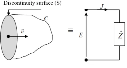
2.2. The Impedance Operator
The impedance operator, as shown in Figure 2, is a modal integro-differential operator and presents an alternative to the Green operator in the spectral field. The relation between E⃗ and J⃗ classically takes the form of the Ohm’s law: E⃗ = ˆZ ⃗J orJ⃗= ˆY ⃗E.
Figure 2. Equivalence between the half-space (S+C).
2.3. The Excitation Sources
(a) (b)
Figure 3. (a) Field source, (b) current source.
3. CHOICE OF TRIAL FUNCTIONS: WAVELETS EXPANSION
The testing functions are presented as a superposition of wavelets at several scales and include a scaling function. A Galerkin’s method is then applied to transform the integral equation into algebraic equations in the expansion coefficients.
Wavelet theory is detailed in many books [16–18]. In this section, we concisely list basic wavelet principles.
A multiresolution analysis ofL2(R) is defined as a sequence of closed subspacesV
s ofL2(R),s∈Z.
A unique function ϕ(x) ∈V0 with a typical width of unity, referred to as the scaling function (scalet), with a nonvanishing integral, exists so that the collection{φ(t−k);k∈Z}forms a Riesz (stable) basis of V0.
The collection of functions{φs,k;k∈Z}contains the dilated and translated versions of the mother
wavelet and are defined with
ϕs,k(x) = 2s/2ϕ(2sx−k) (1)
It forms a Riesz basis ofVswhich is the space of all square integrable functions possessing details whose
length scales are not smaller than 2s.
An approximation of an arbitrary function f(x) ∈ L2(R) at a specific resolution of 2−s0 can be
defined as the orthogonal projection of f(x) intoVs0, i.e.,
Ps0(f) = Σk⟨f(x)|ϕs0,k(x)⟩ϕs0,k(x) = Σkas0ϕs0,k(x), (2)
It is desirable to describe a function in terms of its approximation in Eq. (2) and remaining terms containing local measure of the finer details. It is formally facilitated by the fact that there exists a complementary subspace Ws of Vs inVs+1; that is, a space that satisfies
Vs+1 =Vs⊕Ws (3)
The orthogonal projection of a function f(x)∈L2(R) intoWs,
Qs(f) = Σk⟨f(x)|ψs,k(x)⟩ψs,k(x) = Σkds,kψs,k(x), (4)
gives finer details at resolution level 2−s. Consequently, Eq. (3) implies
Ps+1(f) =Ps(f) +Qs(f). (5)
Starting with a coarse approximation at an initially lowest resolution level s0, one can improve the accuracy to any desired stage, up to the resolution level s(+)+ 1, by adding the projections onto the intermediate wavelet subspacesWs as follows:
Psu+1(f) =Ps0(f) + Σ
su
s=s0Qs(f) (6)
Thus, the last equation describes f(x) at the resolution of 2−su in terms of its approximation at the
resolution 2−s0 and its finer details.
The electromagnetic study of a perfectly-conducting body is usually formulated as an integral equation written to describe the current distribution on the body surface with finite size.
Given a multiresolution system defined on R with scaling function ϕ and wavelet ψ, periodic functions {ϕps,k}and {ψps,k} of unit period are given by
ϕps,k(x) = Σl∈Zϕs,k(x−l), s≥0, 0< k≤2s−1 (7)
ψs,kp (x) = Σl∈Zψs,k(x−l), s≥0, 0< k≤2s−1 (8)
For any functionf(x)∈L2([0,1]), we have the following wavelet projection in a periodic system [19, 20]:
P f(x) = Σ2ks=0(−)cs(−),kϕs(−),k(x) + Σ s(+)
s=s(−)Σ 2s−1
k=0 ds,kψs,k(x) (9)
wheres(−) is the coarsest resolution level,s(+) the finest resolution level andkthe translation index [21]. The scale coefficients are calculated for the coarse level of resolutions(−) by:
cs−,k =⟨f |ϕs−,k⟩=
∫
f(x)ϕs−,k(x)dx;∀k∈[0,2s−1] (10)
The wavelet coefficients are calculated for in intermediate resolution levelsby:
ds,k =⟨f |ψs,k⟩=
∫
f(x)ψs−,k(x)dx;∀k∈[0,2s−1] (11)
4. VALIDATION OF NUMERICAL RESULTS
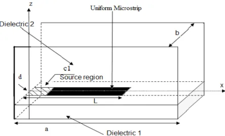
4.1. Formulation of the MR-GEC
The proposed approach will be validated through the study of the structure described in Figure 4. It is an open-end planar microstrip line excited by an arbitrary located voltage source E0 placed on the circuit plane. The dielectric substrate used to analyze shielded microstrip-type structures has been assumed homogeneous, isotropic, and lossless. Its upper face is partially metallized with a uniform zero-thickness conducting strip along the direction of propagation (ox). This structure is embedded in a metallic waveguide whose cross section corresponds to the shape of the circuit. The considered waveguide is infinite in the positive direction of (oz) axis and lossless. It is associated to EEEE boundaries: four perfect electric plates. The characterization of the structure is made by modeling current density with appropriate wavelets used as trial functions.
Figure 4. Open-end microstrip line.
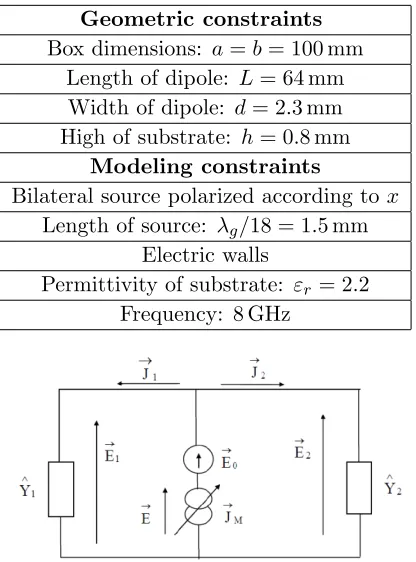
Based on the implementing rules, we can formulate the problem of searching the currentJ flowing in the structure by studying its equivalent circuit. To do this, we bring back different modes propagating in space on the study area, and we transpose vacuum to a dipole representing the admittance of vacuum
ˆ
Y1. The same applies to the ground plane which is replaced by a dipole representative of the admittance shorted ˆY2. We use an arbitrary excitation E⃗0 on the microstrip line subregion. On the plane of the strip, the current density on the metal regionJ⃗M is expressed in terms of trial functions basis. We then
Table 1. Modeling of geometric constraints.
Geometric constraints
Box dimensions: a=b= 100 mm Length of dipole: L= 64 mm Width of dipole: d= 2.3 mm High of substrate: h= 0.8 mm
Modeling constraints
Bilateral source polarized according tox
Length of source: λg/18 = 1.5 mm
Electric walls
Permittivity of substrate: εr= 2.2
Frequency: 8 GHz
Figure 5. Equivalent circuit of the microstrip line.
Let{fmnTE,TM}be the local modal basis of the EEEEE waveguide enclosing the microstrip line [22].
⃗
E0 = V0G⃗(x, y) denotes the electric field excitation, defined on the surface of the planar source according to a distribution G⃗ on a sub-region of the microstrip line and with an amplitude V0.
JM can be expressed in terms of the magnetic fields defined in the discontinuity plane as:
⃗
JM =H⃗1∧⃗n1+H⃗2∧⃗n2=J⃗1+J⃗2 (12) where ⃗n1 and ⃗n2 indicate unit vectors normal to the discontinuity plane and directed toward z > 0 and z <0, respectively. Here, the admittance operators ˆY1 and ˆY2 for region 1 and 2, respectively, are viewed by the discontinuity plane.
Figure 5 describes the electric circuit obtained by the application of GEC modeling to the studied structure, and the generalized Ohm and Kirchhoff laws are then rewritten as equations system:
E0+E2= ˆY2−1J2
E0+E1= ˆY1−1J1
J1+J2=JM
(13)
We then obtain the following system: {
JM =J1+J2=J
E=−E0+ (
ˆ
Y1+ ˆY2 )−1
JM =−E0+ ˆZJM
(14)
Sources and their duals are related as:(
J Ee
) =
(
0 1
−1 Zˆ
) (
E0
Je
)
(15)
This method requires the involvement of a complete set of orthogonal basis functions {|fm,n⟩}m,n=0,N,
shielding [23]. This process also needs to calculate the mode impedances z1
mn and zmn2 , of regions
1 and 2, respectively, at the discontinuity plane. For each medium i ∈ {1,2}, the expressions of the total modal admittance and impedance for TEm,n and TMm,n modes are given respectively by:
TE :yi,T Em,n =
γm,ni jωµ0
TM :yi,T Mm,n =
jωε0 γi m,n ⇒
TE :zm,ni,T E =
1
ym,ni,T E
TM :zm,ni,T M =
1
ym,ni,T M
(16)
with
γm,ni =√(maΠ)2+(nbΠ)2−ki2
k2
i =
{
k20; (i= 1(vacuum))
k20εr; (i= 2(dielectric))
.
When the structure along thezaxis is terminated in the metallic wall (short circuit), the admittance seen by each mode at the interface is given by:
Ym,nα,i =ym,nα,i coth(γm,ni hi
)
, (17)
hi is the thickness of the mediumi, in our case,i= 2;hi =h (the medium is the dielectric).
If a termination was an open circuit (no metallic wall at the end of the mediumi), the admittance seen by each mode at the interface is given by:
Ym,nα,i =yα,im,n (18) In our case, the medium iis the vacuum.
The total impedance seen by each mode at the interface is given by:
Zm,nα = 1
Yα m,n
= 1
Ym,nα,1+Ym,nα,2
; α∈ {TE,TM} (19)
The expression of the impedance operator is expressed as: ˆ
Z = Σm,n|fm,n⟩zm,n⟨fm,n|= Σm,nfm,nTE
⟩
zm,nTE⟨fm,nTE|+ Σm,nfm,nTM
⟩
zm,nTM⟨fm,nTM| (20) At this stage, we can project the unknownJ⃗M (current) on the basis of trial functions, so we will express
it with series of scaling and wavelets functions (test functions) and then write:
JM(x) = Σ2
s(−)
k=0 cs(−),kϕs(−),k(x) + Σ s(+)
s=s(−)Σ 2s−1
k=0 ds,kψs,k(x) (21)
wheres(−) is the coarsest level and s(+) the finest level.
We use the Galerkin method to solve Eq. (21) numerically. The method consists in determining the system matrix from the equivalent circuit and makes projections based on test functions. The resulting matrix equation is written in this form:
[
[Zϕϕ] [Zφψ]
[Zψϕ] [Zψψ]
] [ [c
s(−),k
]
k
[ds,k]s,k
] =
[
[⟨ϕs(−),k′, E0⟩]k′
(⟨ψs′,k′, E0⟩)s′,k′
]
⇒A·X=B (22a)
where,
Zϕϕ
(
k′, k) = ⟨ϕs(−),k′(x),Zϕˆ s(−),k(x)⟩
= ΣNBTEm,n ⟨ϕs(−),k′(x), fm,nTE(x))⟩zTEm,n⟨fm,nTE(x), ϕs(−),k(x))⟩
+ΣNBTMm,n ⟨ϕs(−),k′(x), fm,nTM(x))⟩zm,nTM⟨fm,nTM(x), ϕs(−),k(x))⟩ (22b)
Zϕψ
(
k′, k) = ⟨ϕs(−),k′(x),Zψˆ s,k(x)⟩
= ΣNBTEm,n ⟨ϕs(−),k′(x), fm,nTE(x))⟩zTEm,n⟨fm,nTE(x)), ψs,k(x)⟩
+ΣNBTMm,n ⟨ϕs(−),k′(x), fm,nTM(x))⟩zm,nTM⟨fm,nTM(x)), ψs,k(x)⟩ (22c)
Zψϕ
(
k′, k) = ⟨ψs′,k′(x),Zϕˆ s(−),k(x)⟩
= ΣNBTEm,n ⟨ψs′,k′(x), fm,nTE(x))⟩zTEm,n⟨fm,nTE(x)), ϕs(−),k(x)⟩
Zψψ
(
k′, k) = ⟨ψs′,k′(x),Zψˆ s,k(x)⟩
= ΣNBTEm,n ⟨ψs′,k′(x), fm,nTE(x))⟩zm,nTE⟨fm,nTE(x)), ψs,k(x)⟩
+ΣNBTMm,n ⟨ψs′,k′(x), fm,nTM(x))⟩zm,nTM⟨fm,nTM(x)), ψs,k(x)⟩ (22e)
The input impedance seen by the source is determined by:
Zin= ⟨
E0|E0⟩
⟨E0|JM⟩
=(BTA−1B)−1 (23)
The reflection coefficient is then expressed as:
S11=
Zin−Zc
Zin+Zc
(24)
whereZC = 50 Ω is also the characteristic impedance of microstrip line.
Optimization of the Evaluation of Matrix Elements
In the application of the MR-GEC approach, some improvements can be realized to speed up our method. Indeed, wavelets are localized functions whose support is too narrow for the finer resolution which generates a strong interaction between the elements of the matrix. In addition, wavelets may not have analytical expressions which oblige us to perform additional treatments to evaluate the impedance matrix. Here we present the numerical implementation of the presented MR-GEC.
In the general structure of the matrix, we are led to the calculation of the following two terms as basic functions and test are real functions:
fmn,ϕα
s(−),k = ⟨ϕs(−),k(x), f
αx
m,n(x, y)⟩; ∀k∈[0,2s(−)−1] (25a)
fmn,ψα
s,k = ⟨ψs,k(x), f
αx
m,n(x, y)⟩; ∀s∈[s(−), s(+)] ∀k∈[0,2s−1] (25b)
where,
fmnαx(x, y) =Nxαfmx(x)fnx(y); α∈ {TE,TM} are the basis functions in the longitudinal direction.
The corresponding terms described with Eq. (25a) are first computed with scaling function at a fine resolution level (s(+) + 1).
fm,ϕs(+)+1,k =⟨ϕs(+)+1,k(x), f
x
m(x)⟩; k∈
[
0,2s(+)+1−1 ]
(26)
As we use the periodic wavelets, a linear mapping relation between the length of the microstrip line and [0,1] is made. We can simplify the evaluation of the inner products and make the calculation faster by applying the one point quadrature rule [24–26]:
⟨f(x), ϕ(s, k)(x)⟩ ≈mf(k/2s); m= ∫ +∝
−∝ ϕ(x)dx (27)
The accuracy of this approximation increases with the level of resolutionsand negligible for the Coifman family.
The next step in our algorithm is to apply the pyramidal algorithm of Mallat (Discrete Wavelet Transform DWT) from the fine resolution level (s(+) + 1) to the coarse resolution level s(−). This decomposition allows reducing the CPU time for the impedance matrix fill in [27].
The last step of the computation of the impedance matrix is a thresholding procedure. This is done in order to reduce the memory storage and matrix time computation. This step is to look for the largest element of the impedance matrix Z. The other elements are thus compared to this reference value multiplied by a thresholding parameterδ. Thresholding rule is defined as follows:
Zi,j = 0 if |Zi,j|<|Zmax| ×δ (28)
The compression rate is defined as follows:
TC (%) = NBzero
4.2. Validation of the Analysis Method
In order to validate the detailed approach, a MATLAB code has been written to analyze the microstrip line. A study of convergence is performed to verify the stability of the method.
Let us consider the structure given in Figure 4 to calculate the input impedance using the MR-GEC procedure. A convergence study of Zin based on the basis functions is performed, knowing that the
Daubechies family of wavelets (db5) is used as test functions describing the metal part for different levels of resolutions, and the following result is obtained as shown in Figure 6.
We observe in Figure 6 that beyond a mesh size of the order of λg
30 and 400 basis functions (200 TE guide’s modes +200 TM guide’s modes), the results stabilize. In the remainder of the study, the number of basis functions retained is 600, and the level of discretization retained is about λg
50 which corresponds to a resolution level s = 6, so 64 scaling functions and 64 wavelet functions are used as test functions (128 trial functions). This level of resolution is the minimum mesh size to ensure good accuracy of numerical calculation and stability of the obtained results.
Input ImpedanceZin is calculated for the frequencies between 2–8 GHz.
Figure 6. Numerical convergence of the input impedance evaluated by the MR-GEC method as a function of number of cells per guided wavelength atf = 8 GHz.
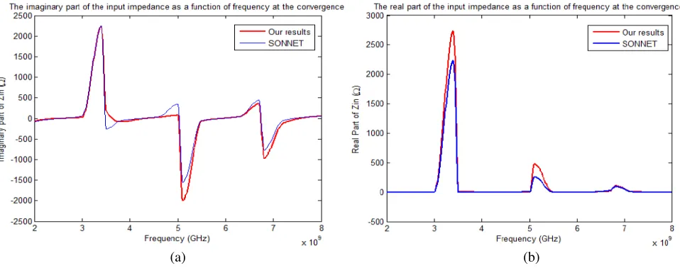
(a) (b)
Figure 7. The imaginary and real parts ofZin evaluated by the MoM-GEC method at the convergence
Figure 8. Numerical convergence of current as a function of wavelet functions number (db5) at
f = 8 GHz.
Figure 9. Numerical convergence of current as a function of basis functions number (db5) atf = 8 GHz and using 128 trial functions (db5).
The comparison between our results and those calculated by using SONNET simulation tools (Figure 7(a) and Figure 7(b)) show that they have the same graphs against the frequency.
The behavior of Zin as a function of frequency allows determining the resonance frequency of the
studied structure. These frequencies are in good agreement with electromagnetic theory that between two distinct resonances. We should assure a difference equal to λ0
2 ≈18.7 mm.
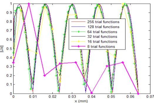
Figure 8 represents the current behavior as a function of the resolution level (number of trial functions) of the db5 wavelet’s family along the xdirection dependence.
We remark that the current convergence is obtained for 128 trial functions (which correspond to a resolution level of wavelets equal to 6).
Figure 9 represents the current behavior as a function of basis functions number. It is shown that the current convergence is obtained starting from 200 basis functions.
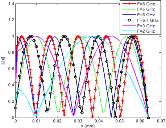
Figure 10. Representation of the current density in the direction of propagation at 8 GHz.
Figure 11. Representation of the current density as a function of frequency.
Table 2. Microstrip line characteristics.
LineCalc (HP-MDS) MoM GEC+wavelets R. Loison [26]
εeff 1.90 1.929 1.92
λg 27.2 27 27.05
λg.
Figure 11 shows the agreement between our results, those obtained by Loison [26] and the results calculated by the conventional moment method.
5. GAIN IN STORAGE MEMORY COST AND COMPUTATIONAL TIME
In this paragraph, we highlight the benefits of using wavelet trial functions in storage memory cost and reducing computational time compared to traditional MoM method. Indeed, the computational time needed by MoM is as [29]:
TMoM=A+BP +CP2+DP3 (30)
P is unknowns’ number. A,B,C and D are constants independent ofP.
A accounts for the simulation set-up time. The meshing of the structure leads to the linear term BP. The filling of the system matrix is responsible for the quadratic term, and solving the matrix equation for the cubic term. The values ofA,B,CandDdepend on the problem at hand. The number of operations needed by MoMNop-MoM is evaluated using [30]:
Nop-MoM≈O (
P3) (31)
To show the gain of the MR-GEC compared to the MoM, we need to evaluate the cost of the new approach required to compute the input impedance.
The parameters used are the following:
- Ts: Computational time of⟨gp|fn⟩.
- Tc: Computational time of multiplication or addition.
- Ti(q): Time inversing of a square matrix includingq2 elements.
- P: Number of test functions characterizing the structure. - N: Number of waveguide modes.
The time used by the MoM-GEC to compute the input impedance of a planar microstrip structure is as:
TMoM GEC =N ×P×Ts+
[
(N + 1)×P2+P]×Tc+Ti(P) +δ (32)
So, in the MoM-GEC, the number of operationsNop−MoM GEC can be expressed as:
Nop−MoM GEC≈O(P2) (33)
We can deduct that Nop−MoM GEC ≪Nop−M oM chiefly when studying large structure with significant
number of test functions. This reduction in number of operations leads then to a reduction in the computational time.
Obviously, in MoM-GEC, the same computational time in the impedance matrix fill in is needed as the conventional moment method since a direct scheme based on a standard numerical integration is used to compute each element of the matrix, and the wavelet functions, which have localized supports, must be computed and stored.
Fortunately, we can take advantage of MALLAT’s algorithm when using wavelets as trial functions. In this paper, an indirect implementation scheme is used to significantly improve the cost of the matrix fill in.
In the MoM GEC method, to compute all matrix elements, we have to computeN ×P times the inner product⟨gp|fn⟩forN modes in the modal basis andP different test functions.
However, according to Eq. (25) and Eq. (26), we need only to calculate fm,ϕs(+)+1,k which can be
approximated by applying the one point quadrature rule.
At the finest resolution level (s(+) + 1), for each value of m ∈[1, N], the vector of P = 2s(+)+1 coefficients (fm,ϕ
s(+)+1,k;k= 0,1, . . . ,2
s(+)+1−1) is filtered byh
kandgkemploying 2LP multiplications
and 2L(P −1) additions [34], where L is the filter length.
The number of required operations is divided by two with regard to the previous stage, due to the data decimation.
Therefore, the total number of multiplications used to compute all scalar products ⟨gp|fn⟩ is
Nop mult= 2LN(P +P2 +P4 +. . .+2sP(−) = 4LN P
(
1−21−s(−)).
Using periodic wavelets and GEC modeling, the computational time required by MR-GEC to solve a proposed problem is as:
TMR GEC= [
(N + 1)×P2+P+Nop mult+Nop add ]
×Tc+Ti(P) +δ (34)
In the adopted approach, after applying a threshold and by discarding all elements smaller than a predetermined threshold δ, the impedance matrix will be converted into a very sparse matrix. Then, the use of wavelets as trial functions in the MoM GEC method produces a sparse impedance matrix which may be solved rapidly thanks to the existence of several efficient techniques.
For such problems, wavelets can be used to obtain a solution inO(PlogP) operations, whereP is the number of unknowns [31, 32]. This is in contrast with a cost ofO(P3) for a dense matrix inversion orO(P2) per dense matrix-vector multiply in an iterative solution such as conjugate-gradient.
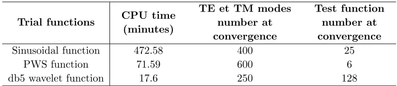
The comparison of the computing time of simulation obtained by using this technique with sinusoidal, piecewise sinusoidal basis functions (PWS) and wavelet test functions is shown in Table 3.
Table 3. Comparison of computational time.
Trial functions CPU time (minutes)
TE et TM modes number at convergence
Test function number at convergence
Sinusoidal function 472.58 400 25
PWS function 71.59 600 6
db5 wavelet function 17.6 250 128
There is a noticeable improvement in the required computing time for calculating the input impedance in our proposed method despite the relatively high number of wavelets functions. For instance, at the frequency of 8 GHz, the computing time in a 2.6 GHz Pentium IV processor with 2 Go of RAM is about 17.6 minutes for MR GEC and 71.59 minutes for MoM GEC with PWS test functions and 472.58 minutes for MoM GEC with sinusoidal test functions.
At this point, the CPU time by our technique represents 96% in relation with the one obtained by sinusoidal functions and 75% with PWS functions.
This contribution in considerable saving in computing time will be more apparent in the study of more complex structures formed by several metallization and with no invariance.
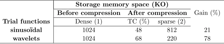
The memory storage is also reduced due to the sparsity of the impedance matrix which is reached by using the thresholding technic.
Figure 12 depicts the compression rate T C(%) for the MOM GEC with sinusoidal functions and MR GEC.
It is shown that the performances obtained with the two types of test functions are not identical. For the simulation of the line, it is possible to achieve a compression rate of 68% with wavelets and only 48% with sinusoidal test functions.
Figure 13 depicts the current’s behavior on the microstrip line obtained by sparse matrices for different values of thresholding parameterδ.
In comparison with the exact solution obtained by uncompressed impedance matrix, the result computed by using the sparse matrix with until 68% nonzero entries demonstrates excellent accuracy. A good precision is always detected when the used number of the nonzero entries reaches 68.2%.
Owing to its sparsity, the impedance matrix, evaluated using wavelet functions, is stored with 220 KO of memory, whereas it would have required 1024 KO to store the dense matrix.
Figure 12. Compression rate of the matrix impedance for two types of test functions at 8 GHz.
Figure 13. Compression effect on the current distribution.
Table 4. Comparison of storage memory of the impedance matrix of a microstrip line at 8 GHz.
Storage memory space (KO)
Gain (%)
Before compression After compression Trial functions Dense (1) TC (%) sparse (2)
sinuso¨ıdal 1024 48 812 21
wavelets 1024 68 220 78
6. CONCLUSION
In this paper, we detail an integral method based on MoM to study microstrip circuits. This original, simple but rigorous approach is obtained by the use of the generalized equivalent circuit modeling based on the impedance operator. Consequently, the electromagnetic problem is transposed to electrical one. To make the proposed method more efficient and obtain a significant reduction in required memory resources, periodic wavelets are used as trial functions in the representation of the unknown current.
In fact, wavelets are characterized by the number of vanishing moments to cancel a significant number of terms of the impedance matrix and thus obtain a sparse matrix and a remarkable gain in memory storage. This gain is enhanced by thresholding operation without affecting the accuracy of found results. Further, the use of the Mallat algorithm allowed us to obtain a gain in computation time thanks to an indirect calculation of the different scalar products.
a numerical analysis of current distribution. A good agreement with technical literature and with those obtained by the software momentum of ADS and the software SONNET was observed which proves the efficiency of the present method.
The technique described in this paper could be extended to model active circuits, multilayer antennas and arrays.
REFERENCES
1. Itoh, T. and M. Menzel, “A full-wave analysis method for open microstrip structures,”IEEE Trans. Antennas Propagat., Vol. 29, 63–68, Jan. 1981.
2. Baudrand, H., “Tridimensional methods in monolithic microwave integrated circuits,” SMBO Brazilian Symposium NATAL, 183–192, Jul. 27–29, 1988.
3. Baudrand, H., “Representation by equivalent circuit of the integral methods in microwave passive elements,” 20th EMC, Budapest, Sep. 10–14, 1990.
4. Harrington, R. F., Field Computation by Moment Methods, Wiley-IEEE Press, Apr. 1993. 5. Zhou, P. B., Numerical Analysis of Electromagnetic Field, 1st Edition, Springer, 1993.
6. Mekkioui, Z. and H. Baudrand, “A full-wave analysis of uniform microstrip leaky-wave antenna with arbitrary metallic strips,”Electromagnetics, Vol. 28, No. 4, 296–314, 2008.
7. Aubert, H. and H. Baudrand, “L’Electromagn´etisme par les sch´emas ´equivalents,” Cepadu`es Editions, 2003.
8. Xiang, Z. and Y. Lu, “An effective wavelet matrix transform approach for efficient solutions of electromagnetic integral equations,” IEEE Trans. Antennas Propagat., Vol. 45, Aug. 1997.
9. Loison, R., R. Gillard, J. Citerne, and G. Piton, “Application of the wavelet transform for the fast computation of a linear array of printed antennas,” European Microwave Conf., Vol. 2, 301–304, Amsterdam, The Netherlands, 1998.
10. Oberschmidt, G. and A. F. Jacob, “Accelerated simulation of planar circuits by means of wavelets,” European Microwave Conf., 305–310, Amsterdam, The Netherlands, 1998.
11. Wang, G., and G.-W. Pan, “Full wave analysis of microstrip floating line structures by wavelet expansion method,”IEEE Trans. on Microw. Theory Tech., Vol. 43, No. I, 131–142, 1995.
12. Chui, C. K. and E. Quak, “Wavelets on a bounded interval,” D. Braess and C. L. Schumaker, (eds.), “Numerical methods of approximation theory,” Vol. 9, 53–75, 1992.
13. Steinberg, B. Z. and Y. Leviatan, “On the use of wavelet expansions in the method of moments,” IEEE Trans. Antennas Propagat., Vol. 41, No. 5, 610–619, 1993.
14. Zhu, X., T. Sogaru, and L. Carin, “Three-dimensional biorthogonal multiresolution time-domain method and its application to electromagnetic scattering problems,” IEEE Trans. Antennas Propagat., Vol. 51, No. 5, 1085–1092, May 2003.
15. Baudrand, H.,Circuits Passifs en Hyperfr´equences, Editions C´epadu`es, Jan. 2001.
16. Aguili, T., “Mod´elisation des composants S. H. F planaires par la m´ethode des circuits ´equivalents g´en´eralis´es,” Thesis, National Engineering School of Tunis ENIT, May 2000.
17. Wang, G., “On the utilization of periodic wavelet expansions in the moment methods,” IEEE Trans. on Microw. Theory Tech., Vol. 43, No. 10, Oct. 1995.
19. Pan, G. W. and X. Zhu, “The application of fast adaptive wavelet expansion method in the computation of parameter matrices of multiple lossy transmission lines,”IEEE Trans. on Microw. Theory Tech., Vol. 1, 29–32, 1994.
20. Meyer, Y., “Ondelettes sur I’intervalle,”Rev. Math. Iberoamer., Vol. 7, 115–143, 1991.
21. Baudrand, H., “Introduction au calcul des circuits microsondes,” Cepadues Ed., ENSEEIHT, Toulouse, 1994.
22. Boggess, F. and J. Narcowich,First Course in Wavelets with Fourier Analysis, Wiley, Oct. 2009. 23. Pan, G. W.,Wavelets in Electromagnetics and Device Modeling, Wiley, New York, 2003.
24. Daubechies, “Ten lectures on wavelets,” Society for Applied Mathematics Philadelphia, Pennsylvania, 1992.
25. Beylkin, G., R. R. Coifman, and V. Rokhlin, “Fast wavelet transforms and numerical algorithms — I,” Yale Univ. Tech. Rep., YALEU/DCS/RR-696, Aug. 1989, Commun. Pure Appl. Math., Vol. XLIV, 141–183, 1991.
26. Loison, R., “Utilisation de l’analyse multir´esolution dans la m´ethode des moments. Application `
a la mod´elisation de r´eseaux d’antennes imprim´ees,” Ph.D. Thesis, National Institute of Applied Sciences, Jan. 2000.
27. Zhu, J., “Development of sensitivity analysis and optimization for microwave circuits and antennas in the frequency domain,” Master Thesis, Mcmaster University, Amilton, Ontario, Jun. 2006. 28. N’Gongo, R. S. and H. Baudrand, “Application of wave concept iterative procedure in planar
circuits,”Recent Res. Devel. Microwave Theory and Technique, Vol. 1, 187–197, 1999.
29. Beylkin, G., R. Coifman, and V. Rokhlin, “Fast wavelet transforms and numerical algorithms I,” Comm. Pure Appl. Math., Vol. 44, 141–183, 1991.
30. Alpert, B., R. Coifman, and V. Rokhlin, “Wavelet-like bases for the fast solution of second-kind integral equations,” SIAM J. Sci. Comput., Vol. 14, No. 1, 159–184, Jan. 1993.
31. Beylkin, G., R. R. Coifman, and V. Rokhlin, “Fast wavelet transforms and numerical algorithms — I,” Yale Univ. Tech. Rep., YALEU/DCS/RR-696, Aug. 1989, Commun. Pure Appl. Math., Vol. XLIV, 141–183, 1991.
32. Alpert, B., R. Coifman, and V. Rokhlin, “Wavelet-like bases for the fast solution of second-kind integral equations,” SIAM J. Sci. Comput., Vol. 14, No. 1, 159–184, Jan. 1993.
33. Chang, X. and L. Tsang, “Fast and broadband modeling method for multiple vias with irregular antipad in arbitrarily shaped power/ground planes in 3-D IC and packaging based on generalized foldy-lax equations,” IEEE Transactions on Components, Packaging and Manufacturing Technology, Vol. 4, 685–696, 2014.