Reduced Capacitance of Single Phase Four-Switch Rectifier with
Fuzzy Controller
Madupu Rajendar & V.Sunil Kumar
1m.Tech, St.Martin‟s Engineering College Affiliated To Jntuh, Hyderabad, Telangana, India. 2associate Professor, St.Martin‟s Engineering College Affiliated To Jntuh, Hyderabad, Telangana, India
ABSTRACT- In this project we are implementing a single-phase four-switch rectifier with considerably reduced capacitance. In this paper the rectifier consists of one conventional rectification leg and one neutral leg linked with two capacitors that split the DC bus. According to the ripple energy inside the rectifier is diverted into the lower split capacitor in order that the voltage throughout the upper split capacitor, designed to be the DC output voltage, has very small ripples. Here we are utilizing the fuzzy logic controller because of its better performance when comparing to the other controller. Such as, the fuzzy controller is the most suitable for the human decision-making mechanism, providing the operation of an electronic system with decisions of experts. There the voltage throughout the lower capacitor is designed to have big ripples on purpose so that the entire capacitance wished is considerably reduced and especially dependable film capacitors, as opposed to electrolytic capacitors, can be utilized. The ripple energy in the rectifier is diverted into the lower split capacitor so that the voltage across the upper split capacitor, designed to be the DC output voltage, has very small ripples. The voltage across the lower capacitor is designed to have large ripples on purpose so that the total capacitance needed is significantly reduced and highly reliable film capacitors, instead of electrolytic capacitors, can be used. By using the simulation results we can analyze the performance of the proposed strategy.
Index Terms—Electrolytic capacitors, neutral leg, reliability, ripple eliminator, single-phase rectifiers, voltage ripples.
I. INTRODUCTION
More and more microgrids are now connected to the public grid and various loads through power converters [1]. For both AC and DC microgrids, single-phase rectifiers are often needed when supplying DC loads. Such rectifiers are expected to have high power density, high efficiency, high reliability and low costs. As a result, the study of single-phase rectifiers has attracted more and more attention. Conventionally, bulky electrolytic capacitors are required for single-phase rectifiers to produce smooth DC-bus voltage, due to the pulsating input power.
However, the volume and weight of bulky electrolytic capacitors could be a serious problem for volume-critical and/or weight-critical applications, such as electrical vehicles [4] and aircraft power systems [5]. What is worse is that electrolytic capacitors, known to have limited lifetime, are one of the most vulnerable components in power electronic systems. In general, the
reduction of electrolytic capacitors can be achieved in four approaches. One approach is to inject harmonic currents to suppress fluctuations of input energy by changing control strategies for existing power switches in rectifiers.
The objective of this paper are
1. To introduces the rectifier under investigation. 2. To significantly reduce DC-bus capacitors is discussed.
3. The associated control strategies are developed. In order to achieve the minimal capacitance, the selection criteria of the split capacitors are then discussed .
4. The impact of the different voltages across the split capacitors are analyzed.
Different from other solutions, an AC capacitor instead of a DC capacitor is used to handle ripple energy, which also reduces the voltage stress on the switches. The rectifier only uses four switches, which is similar to a conventional bridge PWM rectifier, but the switches are formed as a rectification leg and a neutral leg and operated differently from a conventional full-bridge rectifier.
II. THE SINGLE-PHASE RECTIFIER UNDER INVESTIGATION
The rectifier proposed in the preliminary version of this paper is investigated further in this paper. It consists of one rectification leg and one neutral leg, as shown in Figure 1.
The total capacitance could be significantly reduced because the ripple energy is diverted from the output capacitor to the other capacitor, which could have high voltage ripples. By diverting all the ripple power to the lower capacitor C−, the output voltage V+ can become ripple free, which means the output capacitance C+ can be reduced a lot because it does not need to process any low frequency ripple energy. Importantly, the capacitor C− can also be significantly reduced because its voltage is not supplied to any loads so it can be designed to have large ripples on purpose.
III. REDUCTION OF THE BULKY DC-BUS CAPACITORS
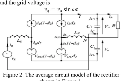
In order to clearly show how to significantly reduce the DC-bus capacitors, there is a need to analyze the relationship between the ripple energy and the required capacitors for the investigated rectifier. For this purpose, an average circuit model is built up at first.
A. Circuit Analysis
It is assumed that the DC-bus voltage of the rectifier is 𝑉𝐷𝐶= 𝑉++ 𝑉−
where V+ and V− are the voltages across the split capacitors C+ and C− with respect to the neutral point N and the negative point of the DC bus, respectively. Suppose that the grid current is
𝑖𝑔 = 𝐼𝑔sin 𝜔𝑡 and the grid voltage is
𝑣𝑔 = 𝑣𝑔sin 𝜔𝑡
Figure 2. The average circuit model of the rectifier shown in Figure 1.
In which V g and Ig are the peak values of the grid voltage and current, respectively, and ω is the angular line frequency.
In this paper, the split capacitors are not necessarily the same, so the model in this paper is more generic. Also note that in order to facilitate the exposition in the sequel, the duty cycle of the lower switch of the rectification leg (Q2) and the duty cycle of the upper switch of the neutral leg (Q3) are adopted in the model. According to the average circuit model of the rectifier shown in Figure 2, the capacitor currents can be found as
𝑖𝐶+= 𝑖𝑔 1 − 𝑑2 − 𝐼𝑅− 𝑖𝐿𝑑3
𝑖𝐶−= −𝑖𝑔𝑑2+ 𝑖𝐿(1 − 𝑑3)
and the neutral current iL can be found as
𝑖𝐿= 𝑖𝐶−− 𝑖𝐶++ 𝑖𝑔− 𝐼𝑅
In order to obtain the unity power factor, the two switches Q1 and Q2 can be operated complementarily to track the reference of the grid current, which is in phase with the grid voltage. Since the switching frequency is much higher than the line frequency, the duty cycle of Switch Q2 can be calculated in the average sense as
𝑑2= 𝑉+
𝑉𝐷𝐶−
𝑉𝑔
𝑉𝐷𝐶sin 𝜔𝑡
To maintain the DC-bus voltage VDC, according to [26], [29]. Normally, Switches Q3 and Q4 are operated complementarily to split the DC-bus voltage VDC into V+ and V− [1], [21], [30], [31]. The duty cycle of Switch Q3 can be calculated as
𝑑3= 𝑉−
𝑉𝐷𝐶
because the neutral leg is operated as a DC/DC buck converter. Because of the power balance between the AC and DC sides (ignoring the power losses), there is
𝑉𝑔𝑖𝑔
2 = 𝑉+2
𝑅
and the load current is 𝐼𝑅=
𝑉𝑔𝐼𝑔
2𝑉+
which is also the DC component of current I. (4) can then be re-written as
𝑖𝐶+= 𝐼𝑔sin 𝜔𝑡 𝑉−
𝑉𝐷𝐶+
𝑉𝑔
𝑉𝐷𝐶sin 𝜔𝑡 −
𝑉𝑔𝐼𝑔
2𝑉+ −
𝑉−
𝑉𝐷𝐶𝑖𝐿=
𝑉−
𝑉𝐷𝐶𝑖𝑔−
𝑉𝑔𝐼𝑔
2𝑉𝐷𝐶cos 2𝜔𝑡 −
𝑉𝑔𝐼𝑔𝑉−
2𝑉+𝑉𝐷𝐶−
𝑉−
𝑉𝐷𝐶𝑖𝐿
Similarly, (5) can be re-written as 𝑖𝐶−= −𝐼𝑔sin 𝜔𝑡
𝑉+
𝑉𝐷𝐶−
𝑉𝑔
𝑉𝐷𝐶sin 𝜔𝑡 + 𝑖𝐿 1 −
𝑉−
𝑉𝐷𝐶 = − 𝑉+
𝑉𝐷𝐶𝐼𝑔−
𝑉𝑔𝐼𝑔
2𝑉𝐷𝐶cos 2𝜔𝑡 +
𝑉𝑔𝐼𝑔
2𝑉𝐷𝐶+
𝑉+
𝑉𝐷𝐶𝑖𝐿
As is well known, no DC currents could pass through capacitors. As a result, iL should have a DC component so that iC+ and iC− do not have any DC component. It can be found out from (10) and (11) that the DC component of iL is −IR = − V 2g VI + g , i.e., the same value as the load current. If the neutral current iL is controlled to provide the DC component only, that is,
𝑖𝐿= −𝐼𝑅
then the capacitor currents are
𝑖𝐶+= 𝑉−
𝑉𝐷𝐶𝐼𝑔−
𝑉𝑔𝐼𝑔
2𝑉𝐷𝐶cos 2𝜔𝑡
and
𝑖𝐶−= − 𝑉+
𝑉𝐷𝐶𝐼𝑔−
𝑉𝑔𝐼𝑔
2𝑉𝐷𝐶cos 2𝜔𝑡
In addition to the same second-order ripple current -VgIg 2VDC cos2ωt flowing through the split capacitors, the grid current ig is split between iC+ and iC- because in this case
𝑖𝐶++ −𝑖𝐶− = 𝐼𝑔
to reduce the voltage ripples, the current flowing through the capacitors should be regulated differently. For this reason, a different control strategy is proposed in the next subsection.
B. REDUCTION OF DC-BUS CAPACITANCE
The idea is to push the current components of iC+ in (10) through the neutral leg instead of through the upper split capacitor so that iC+ does not contain any fundamental or second order ripple currents. That is to make iC+ = 0, ignoring the switching ripples. Hence, according to (10), the current iL should be controlled to satisfy
𝑖𝐿= 𝑖𝑔−𝑉𝑔𝐼𝑔
2𝑉−cos 2𝜔𝑡 −
𝑉𝑔𝐼𝑔
2𝑉+
On the other hand, iL should also satisfy (6). Hence, in this case, the current flowing through the lower split capacitor should be
𝑖𝐶−= −𝑉𝑔𝐼𝑔
2𝑉−cos 2𝜔𝑡
In other words, it only contains the second-order harmonic component or the second-second-order component only flows through the lower split capacitor. As a result, all the voltage ripples are then diverted to the lower capacitor C−, which would increase the voltage ripples on C−.
IV. CONTROL DESIGN
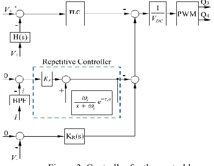
A) Control of the Neutral Leg
The neutral leg should be controlled to maintain the output voltage V+, to remove the ripple components in iC+ and also to remove the fundamental component in iC−.
1) Regulation of the output voltage V+:
Maintaining a stable output voltage V+ with very small ripples at the desired output reference voltage V+ ∗ is a major target. The regulation of the sum of the voltages V+ and V−, i.e. the DC-bus voltage VDC, is the task of the rectification leg and will be discussed in the next subsection. The neutral leg is responsible for splitting the DC-bus voltage into V+ and V−, which are independent from each other.
In order to regulate the output voltage V+, it is measured and put through the hold filter
𝐻 𝑠 =1−𝑒−𝑇𝑠
𝑇𝑠
where T is the fundamental period of the grid voltage, to extract its DC component, as shown in Figure 3. A simple proportional-integral (PI) controller is then applied to regulate the voltage. The output of the PI controller can be converted to PWM signals to drive the switches. The parameters for the PI controller can be selected according to classical design methods for a second-order system, with the characteristic equation given by
𝑠2+𝐾𝑝𝑠
𝐶+ +
𝐾𝑖
𝐶+= 0
where Kp and Ki are the gains of the PI controller. These parameters can be chosen to obtain the damping coefficient of
𝐾𝑝
2 1 𝐶+𝐾𝑖=
1 2
As a result,
𝐾𝑝2= 2𝐶+𝐾𝑖
The relationship between Kp and Ki is mostly related to the capacitor C+. In practice, Kp or Ki can be initially set to small values, which approximately satisfy (15), and then gradually be increased to achieve the desired performance. In this way, both parameters can be well tuned
2) Removal of the ripple components in iC+:
As discussed before, the capacitor current iC+ should be maintained around zero in order to smooth the ripples of the output voltage V+.
In order to reduce the stress on the switches, a repetitive controller is applied in this paper as shown in the dashed box of Figure 3. The repetitive controller consists of a proportional controller Kr and an internal model given by
𝐶 𝑠 = 𝐾𝑟
1−𝜔 𝑟
𝑠+𝜔 𝑟 𝑒−𝜏𝑑 𝑠
where τd is designed based on the analysis as
𝜏𝑑 = 𝜏 −
1 𝜔𝑖
= 0.0196
with ωi = 2550, τ = 0.02 s. Note that the regulation of V+ deals with the DC component but the removal of the ripple components of iC+ deals with non-DC components.
Figure 3. Controller for the neutral leg In general, the adoption of the BPF does not lead to any resonance of the controllers with the rectifier.
Removal of fundamental component in iC
component. However, according to (6), when i = 0, there is
𝑖𝑔 = 𝑖𝐿− 𝑖𝐶−+ 𝐼𝑅 𝐾𝑅 𝑠 =𝑠2+2𝜉𝜔𝐾2𝜉𝜔𝑠+ 𝜔 𝑠 2
which means that the grid current ig could flow through the inductor LN and the capacitor C− if not controlled properly. This can be achieved by forcing the fundamental component of V − to be zero, as shown in Figure 3. The following resonant controller
𝐾𝑅 𝑠 =
𝐾2𝜉𝜔𝑠
𝑠2+2𝜉𝜔𝑠+ 𝜔 2
with ξ = 0.01, h = 1, and ω = 2πf, can be adopted. The output of the resonant controller is then added onto the outputs of the other two controllers before sending to the PWM conversion block, as shown in Figure 3. These should be avoided.
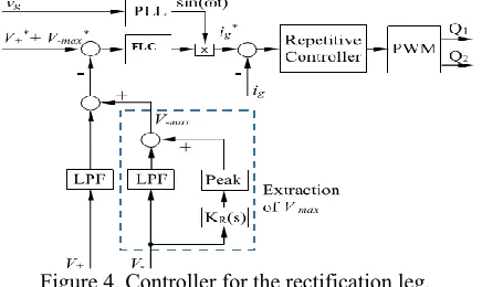
CONTROL OF THE RECTIFICATION LEG
The control of the rectification leg is very similar to that of conventional half-bridge rectifiers, which is mainly used to regulate the grid current and to control the whole DC bus voltage. To be more precise, the grid current is expected to be in phase with the grid voltage and also to be clean with low harmonics.
Figure 4. Controller for the rectification leg. For this purpose, the maximum DC-bus voltage should be extracted at first. Since the voltage V+ is controlled to be more or less pure DC without second-order components, it is only required to extract the maximum value of the voltage V−, which can be obtained by adding the DC component with the peak voltage of the ripple component, as shown in Figure 4.
B) STABILITY OF THE SYSTEM
Because of the decoupled nature of the controllers for the two legs, the stability of the system can be easily guaranteed. The controller for the rectification leg has a very typical structure, which is very mature and widely used in industry.
V. SELECTION OF COMPONENTS A. Selection of Capacitor C
As demonstrated in [9], [24], the total ripple energy stored in the split capacitors over a charging period for single-phase rectifiers with the unity power factor is
𝐸𝑟 =𝑉𝑔𝐼𝑔
2𝜔
With the proposed strategy, all the ripple energy is now stored on the lower capacitor C− instead of both capacitors C+ and C −. Hence
𝐶−= 2𝐸𝑟
𝑉_𝑚𝑎𝑥2 −𝑉_𝑚𝑖𝑛2
where V −max and V−min are the maximum and minimum voltages of V−, respectively. A small capacitor means that high V−max and/or low V−min is needed.
B. Selection Of Inductor Ln
The maximum peak-peak current ripple △iLm on the inductor LN is reached when the duty cycle d3 reaches the maximum, which is when the voltage V− reaches the maximum. That is
∆𝑖
𝐿𝑚=
𝑉+𝑑3𝑚𝑎𝑥𝐿𝑁𝑓𝑆
=
𝑉+𝑉−𝑚𝑎𝑥
𝐿𝑁𝑓𝑆 𝑉++𝑉−𝑚𝑎𝑥
For the given maximum allowed ripple current △iLm, the minimum inductance is
𝐿𝑁𝑚𝑖𝑛 =∆𝑖 𝑉+𝑉−𝑚𝑎𝑥
𝐿𝑚𝑓𝑆 𝑉++𝑉−𝑚𝑎𝑥
The inductance can be reduced if the switching frequency fs is increased. When choosing the magnetic core for the inductor, the DC current component in iL should be taken into consideration to avoid saturation.
C. Selection of Capacitor C+
When Q3 is turned on, C+ is discharged through LN and the maximum ripple current is given the peak-peak switching ripple voltage across the capacitor C+ is
∆𝑉+𝑠=
∆𝑖𝐿𝑚
8𝐶+𝑓𝑠+ ∆𝑖𝐿𝑚𝑅𝐶 =
1
8𝐶+𝑓𝑠+ 𝑅𝐶+
𝑉+𝑉−𝑚𝑎𝑥
𝐿𝑁𝑓𝑆 𝑉++𝑉−𝑚𝑎𝑥
where RC+ is the equivalent series resistance (ESR) of the capacitor C+. The second part, i.e. △iLmRC+, is caused by the ESR of the capacitor. Since RC+ is often negligible for film capacitors, (26) becomes
𝐶+𝑚𝑖𝑛 ≈ ∆𝑖𝐿𝑚
8𝑓𝑠∆𝑉+𝑠𝑚
for the given maximum switching ripple voltage △V+sm and the maximum ripple current △iLm. Note that increasing the switching frequency reduces C+.
D. Design Example
Here, an example is given for demonstration. The selected components, as summarized in Table I, are also used when building up the test rig.
Table I
If a conventional single-phase full-bridge rectifier is adopted, then the DC-bus capacitor should be larger than Vg I g 2ω△V −V−ave ≈ 740 µF in order for the output ripple voltage to be maintained lower than 5V. For capacitors at this level, electrolytic capacitors are often needed.
VI FUZZY LOGIC CONTROLLER
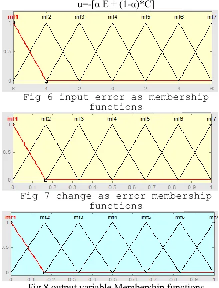
In FLC, basic control action is determined by a set of linguistic rules. These rules are determined by the system. Since the numerical variables are converted into linguistic variables, mathematical modeling of the system is not required in FC.
Fig.5.Fuzzy logic controller
The FLC comprises of three parts: fuzzification, interference engine and defuzzification. The FC is characterized as i. seven fuzzy sets for each input and output. ii. Triangular membership functions for simplicity. iii. Fuzzification using continuous universe of discourse. iv. Implication using Mamdani‟s, „min‟ operator. v. Defuzzification using the height method.
TABLE III: Fuzzy Rules
Fuzzification: Membership function values are assigned to the linguistic variables, using seven fuzzy subsets: NB (Negative Big), NM (Negative Medium), NS (Negative Small), ZE (Zero), PS (Positive Small), PM (Positive Medium), and PB (Positive Big). The Partition of fuzzy subsets and the shape of membership CE(k) E(k) function adapt the shape up to appropriate system. The triangular shape of the membership function of this arrangement
presumes that for any particular E(k) input there is only one dominant fuzzy subset. The input error for the FLC is given as
E(k) = Pp h (k )−Pp h (k −1)
Vp h (k )−Vp h (k −1)
CE(k) = E(k) – E(k-1)
Inference Method: Several composition methods such as Max–Min and Max-Dot have been proposed in the literature. In this paper Min method is used. The output membership function of each rule is given by the minimum operator and maximum operator. Table 1 shows rule base of the FLC.
Defuzzification: As a plant usually requires a non-fuzzy value of control, a defuzzification stage is needed. To compute the output of the FLC, „height‟ method is used and the FLC output modifies the control output. Further, the output of FLC controls the switch in the inverter. To achieve this, the membership functions of FC are: error, change in error and output
The set of FC rules are derived from
u=-[α E + (1-α)*C]
Fig 6 input error as membership functions
Fig 7 change as error membership functions
Fig.8 output variable Membership functions Where α is self-adjustable factor which can regulate the whole operation. E is the error of the system, C is the change in error and u is the control variable.
VII. IMPACT OF DIFFERENT VOLTAGES V+ AND V−
The voltages across the two split capacitors are normally maintained to be the same in similar topologies.
The main objective of the rectification leg is to maintain the grid current to be clean and to be in phase with the grid voltage. According to (7), the maximum and minimum values of the duty cycle of the two switches in the rectification leg are
𝑑2𝑚𝑎𝑥 = 1
𝑉𝐷𝐶 𝑉++ 𝑉𝑔
𝑑2𝑚𝑖𝑛 =
1
𝑉𝐷𝐶 𝑉+− 𝑉𝑔
Since V+, V− > Vg, then d2min > 0 and d2max < 1 can be achieved for any combinations of V+ and V−. According to the average model, the duty cycle of the switch Q2 is
𝑑2= 𝑉+
𝑉𝐷𝐶−
𝑉𝑔
𝑉𝐷𝐶sin 𝜔𝑡 =
1
𝑉++𝑉− 𝑉+− 𝑉𝑔sin 𝜔𝑡
If all the ripple power is provided by the lower capacitor, then(28) becomes
𝑑2= 1
𝑉++ 𝑉−𝑚𝑖𝑛2 +𝑃𝑂𝐶− 1−sin 2𝜔𝑡
𝑉+− 𝑉𝑔sin 𝜔𝑡
where the derivation of V − can be found in [24] for a given load power Po. It is clear that the obtained duty cycle contains a second-order ripple component coming from V−.
Impact on the Neutral Leg
The neutral leg is used for two purposes, i.e. splitting the DC-bus voltage to V+ and V− and diverting the ripple power to the lower capacitor C−. According to the average model, the duty cycle of the switch Q3 can be given as
𝑑2= 1 −
𝑉+
𝑉𝐷𝐶= 1 −
𝑉+
𝑉++ 𝑉−𝑚𝑖𝑛2 +𝜔𝐶 −𝑃𝑂 1−sin 2𝜔𝑡
which is also affected by a second-order ripple component. As long as V− < VDC, which is always true because VDC = V++ V− > V+, V−, the duty cycle d3 can be always achieved by controlling the two switches Q3 and Q4 in an complementary way. Impact on the Current Stress of the Switches
The two voltages can be controlled to be the same. In this case, the average currents of the switches become the same and also, the average currents of the switches become the same too.
Switches and diodes of the neutral leg:
For the neutral leg, there are also two switches and two diodes in total. The current flowing through the neutral leg mainly depends on the inductor current iL. In order to analyze the average currents, similar analysis can be done.
Impact on the Voltage Stress of the Switches
In order to choose suitable switches for both legs, the voltage stress of the switches is another factor to be considered. Compared to the current stress of the switches, it is more straightforward to analyze the voltage stress of the switches.
Impact on Switching Ripples of the Grid Current
Since the switching frequency is much higher than the fundamental frequency, the average grid current over each switching period can be controlled to track its reference, which is a sinusoidal signal. According to [26], the peak-peak switching ripple of the grid current can be given as
∆𝑖𝑔= 𝑉 −
𝑉 𝐷𝐶𝑉𝐷𝐶+𝑉𝑔sin 𝜔𝑡
𝐿𝑔𝑓𝑠 𝑑2=
1
𝐿𝑔𝑉𝐷𝐶 𝑉+𝑉−− 𝑉𝑔
2sin2𝜔𝑡 +
𝑉+−𝑉− 𝑉𝑔
𝐿𝑔𝑓𝑠𝑉𝐷𝐶 sin 𝜔𝑡
Apparently, increasing the inductor and/or increasing the switching frequency could reduce the switching current ripple.
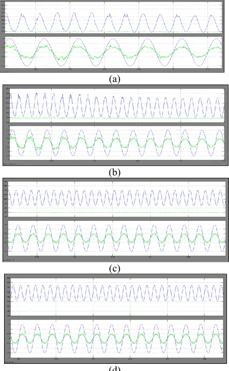
A. STEADY-STATE PERFORMANCE
1) The grid current ig and the DC voltages V+ and V−: The system steady-state performance with V+ ∗ = 200 V is given in Figure 5(a)-(d) for V− ∗max = 600, V− ∗max = 650, V ∗ −max = 700 and V− ∗max = 750, respectively.
(a)
(b)
(c)
(d)
∗max = 600 V, (b) whenV- ∗max = 650 V, (c)when V ∗ -max = 700 V and (d) when V- ∗max = 750 V.
for the cases when the DC voltages V+ and V− were lower than the peak grid voltage and when the controller that removes the fundamental component from iC− was disabled.
Figure 10. Voltage ripples of V+ and V- over a wide range of V-ave.
Figure 11. Deteriorated system performance with V+ ∗ = 200 V when V ∗-max = 500 V
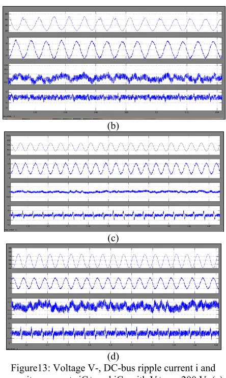
The DC-bus current and the capacitor currents: As mentioned above, the reduction of the voltage ripples is achieved by controlling the AC component i of the DC-bus current I.
Figure 12. Deteriorated system performance when the controller that removes fundamental component from iC-
was disabled (V- ∗max = 700 V)
(a)
(b)
(c)
(d)
Figure13: Voltage V-, DC-bus ripple current i and capacitor currents iC+ and iC- with V+ ∗ = 200 V: (a) when V- ∗max = 600 V, (b) when V- ∗max = 650 V, (c) when V- ∗max = 700 V and (d) when V- ∗max = 750 V.
Figure 14. DC-bus current i and capacitor currents iC+ and iC- over a wide range of V-ave.
(b)
Figure 15. Comparison of (a) without and (b) with the repetitive current controller for the neutral leg.
Due to the diverted 100 Hz current, both the ripples of the output voltage V+ and DC-bus current I are considerably reduced as shown in Figure 15(b).
B. Transient Performance 1) System start-up:
The grid current first increased to charge the capacitors and then the current was maintained well back to its steady-state value after the DC output voltage was settled. The system start-up took about 200 ms, which is only about 10 cycles.
2)Change of the voltage reference:
When the reference of the voltage V+ was changed from 200 V to 300 V, the results are shown in Figure 16.
Figure 16. Transient response when the reference of the voltage V+ was changed from 200 V to 300 V.
3) Hold-up time:
Although the DC-bus capacitors are designed for systems without hold-time requirement, it is still interesting to see how the proposed rectifier responds to a sudden AC power outage.
(a)
(b)
Figure 17. Transient response after a sudden AC power outage with (a) C+ = 5 µF, C- = 10 µF and (b) C+ = 100
µF, C- = 10 µF
shown in Figure 17(b). Indeed, the voltage V+ was decreased at a much slower pace, which took about 42 ms for the voltage V+ to decrease from 200 V to 0 V. Since the main focus of this paper is not about the hold-up time, no further mathematical analysis is made. Interested readers are referred to [17] to see how to design capacitors for single-phase rectifiers with holdup time requirement
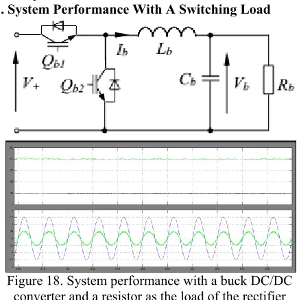
C. System Performance With A Switching Load
Figure 18. System performance with a buck DC/DC converter and a resistor as the load of the rectifier
Apart from resistive loads, rectifiers often have switching devices connected as loads. Such switching devices can include DC/DC converters and DC/AC converters.
VIII. CONCLUSIONS
the operation of an electronic system with decisions of experts. here it is used for the elimination of DC-bus electrolytic capacitors is achieved by the neutral leg of the rectifier without adding any other power components. At the same time, the voltage across the lower capacitor is designed to have large ripples as it is not supplied to any loads. In this case, both capacitors can be reduced to a level that film capacitors are cost effective to be used. The rectification leg of the rectifier is used to maintain the grid current and the DC-bus voltage. As a result, in order to enhance the reliability of power electronic systems, it is highly desirable to minimize the usage of electrolytic capacitors and use highly-reliable small capacitors like film capacitors if possible, while maintaining low voltage ripples. By using simulation result we can verify the proposed system.
REFERENCES
[1] Q.-C. Zhong and T. Hornik, Control of Power Inverters in Renewable Energy and Smart Grid Integration. Wiley-IEEE Press, 2013
. [2] D. Dong, F. Luo, D. Boroyevich, and P. Mattavelli, “Leakage current reduction in a single-phase bidirectional AC–DC full-bridge inverter,” IEEE Trans. Power Electron., vol. 27, no. 10, pp. 4281–4291, 2012. [3] D. Dong, T. Thacker, I. Cvetkovic, R. Burgos, D. Boroyevich, F. Wang, and G. Skutt, “Modes of operation and system-level control of singlephase bidirectional PWM converter for microgrid systems,” IEEE Transactions on Smart Grid, vol. 3, no. 1, pp. 93–104, 2012.
[4] H. Wen, W. Xiao, X. Wen, and P. Armstrong, “Analysis and evaluation of DC-link capacitors for high-power-density electric vehicle drive systems,” IEEE Trans. Veh. Technol., vol. 61, no. 7, pp. 2950–2964, Sept 2012.
[5] R. Wang, F. Wang, D. Boroyevich, R. Burgos, R. Lai, P. Ning, and K. Rajashekara, “A high power density single-phase PWM rectifier with active ripple energy storage,” IEEE Trans. Power Electron., vol. 26, no. 5, pp. 1430–1443, May 2011.
[6] J. Stevens, J. Shaffer, and J. Vandenham, “The service life of large aluminum electrolytic capacitors: effects of construction and application,” IEEE Trans. Ind. Appl., vol. 38, no. 5, pp. 1441–1446, 2002.
[7] L. Han and N. Narendran, “An accelerated test method for predicting the useful life of an LED driver,” IEEE Trans. Power Electron., vol. 26, no. 8, pp. 2249– 2257, 2011.
[8] P. Krein, R. Balog, and M. Mirjafari, “Minimum energy and capacitance requirements for single-phase inverters and rectifiers using a ripple port,” IEEE Trans. Power Electron., vol. 27, no. 11, pp. 4690–4698, Nov. 2012.
[9] K. Yao, X. Ruan, X. Mao, and Z. Ye, “Reducing storage capacitor of a DCM Boost PFC converter,” IEEE Trans. Power Electron., vol. 27, no. 1, pp. 151–160, Jan. 201
[10] O. Garcia, M. Martinez-Avial, J. Cobos, J. Uceda, J. Gonzalez, and J. Navas, “Harmonic reducer converter,” IEEE Trans. Ind. Electron., vol. 50, no. 2, pp. 322–327, 2003
MADUPU RAJENDAR
Completed his B.Tech in Electrical & Electronics Engineering from Tirumala Engineering College Affiliated to JNTU Hyderabad, Telangana, India and is Student of St.Martin‟s Engineering College, Pursuing his M.Tech 2nd Year in EPS (Electrical Power System).His Area of Interest includes Electrical Power Systems, Electrical SubStation, Renewable Energy Systems and High Voltage Engineering.
E-mail id: [email protected]
V.SUNIL KUMAR
Completed B.Tech in Electrical & Electronics Engineering from Syed Hashim College of Science and Technology Affiliated to JNTU Hyderabad and M.Tech in Electrical Power Systems from B.S.A.Crescent Engineering College affiliated to Anna University, Chennai. He is working as Associate Professor in St. Martin‟s Engineering College, Dhullapally, Secunderabad, Telangana. His Area of interest includes Power Systems, FACTS Devices and Renewable Energy Systems.