Temperature Based Behaviour Analysis of SWCNT
Bundle as VLSI Interconnect
Nandita Yadav1, Anup Kumar2 1, 2
Department of Electronics and Communication, Ajay Kumar Garg Engineering College, Ghaziabad
Abstract: The work in this paper describes the analysis delay and power of single walled carbon nanotube (SWCNT) and copper interconnect. Temperature dependent changes in delay for SWCNT have also been discussed. The work has been done on Tanner EDA tool using 22nm technology node. Results shows how SWCNT is a promising interconnect material in future for VLSI application.
Keywords: Carbon Nanotube (CNT), Single Walled Carbon nanotube (SWCNT), Electro migration
I. INTRODUCTION
CNT has got the potential to replace copper for future VLSI interconnects applications. On moving towards deep submicron levels, the resistivity of copper interconnect increases due to several effects [1] like electro migration, surface scattering, skin effect, grain boundary effect. This rapid increase in the resistance of copper poses a serious issue in the future interconnect application.
Thus, to have relieve from such problems it has been decided to replace copper as a interconnect material from CNT. CNT stands
for carbon nanotube and are the allotropes of carbon. They have sp2 bonds similar to graphene. However the properties [1,2] of CNT
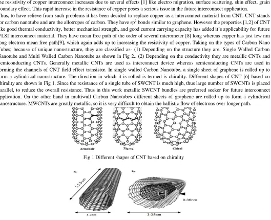
like good thermal conductivity, better mechanical strength, and good current carrying capacity has added it’s applicability for future VLSI interconnect material. They have mean free path of the order of several micrometer [8] long whereas copper has just few nm long electron mean free path[9], which again adds up to increasing the resistivity of copper. Taking on the types of Carbon Nano Tubes; because of unique nanostructure, they are classified as- (1) Depending on the structure they are, Single Walled Carbon Nanotube and Multi Walled Carbon Nanotube as shown in Fig 2.. (2) Depending on the conductivity they are metallic CNTs and Semiconducting CNTs. Generally metallic CNTs are used as interconnect device whereas semiconducting CNTs are used in forming the channels of CNT field effect transistor. In single walled Carbon Nanotube, a single sheet of graphene is rolled up to form a cylindrical nanostructure. The direction in which it is rolled is termed is chirality. Different shapes of CNT [6] based on chirality are shown in Fig 1. Since the resistance of a single tube of SWCNT is much high, thus large number of SWCNTs is placed parallel, to reduce the overall resistance. Thus in this work metallic SWCNT bundles are preferred seeker for future interconnect application. On the other hand in multiwall Carbon Nanotubes different sheets of graphene are rolled up to form a cylindrical nanostructure. MWCNTs are greatly metallic, so it is very difficult to obtain the ballistic flow of electrons over longer path.
Fig 1 Different shapes of CNT based on chirality
[image:2.612.45.574.296.726.2]It is very obvious that as the density of the integrated circuit increases the need to understand effect of temperature increases as well. The operating temperature of most of the densely packaged integrated circuit is more than the room temperature. Several studies have shown that the optical phonon scattering is dominating factor for the temperature above 250K.
II. MODELLINGPARAMETEROFCOPPERINTERCONNECT
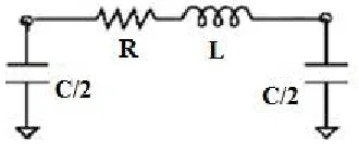
The equivalent circuit model of copper interconnect is shown in Fig 3. The parasitic present in copper interconnect are resistance, inductance and capacitance. These parasitic are calculated using the Windbound TSM
Fig 3 Equivalent circuit model of copper interconnect model.
This model generally contains the global layer interconnect line with coupling above the ground [6]. This model defines the thickness of interconnect as t, width as w, height as h and spacing as s. The equivalent resistance for copper interconnect is given in Eqn 1.
=
( ) = (1 + ( − ))
Here ρ is the resistivity, T is the temperature and T0 is the room temperature. The temperature dependent resistance is given by Eqn 2. The equivalent capacitance of copper interconnect is given by Eqn 3 and equivalent inductance is given by Eqn 4.
Cg
=
2 ln
2
+ +
1
2+
0.22( + )
Here, = where is dielectric permittivity, is relative dielectric permittivity and µ0 is permeability of free space.
III.MODELLINGPARAMETEROFCNTINTERCONNECT
[image:3.612.228.393.173.243.2]Schematic of the interconnect structure using SWCNT is shown in Fig 4 and the equivalent circuit of SWCNT operated is shown in Fig.5.
Fig 4 Equivalent circuit model of SWCNT interconnect
The Landauer- Buttiker formula is used to evaluate [8] the conductance of carbon Nanotube, which is applicable for a one dimensional system having N channels in parallel. In nanotube there are four conducting channels that are in parallel due to spin
=
ℎ+ 2.22 + 0.7ℎ
.
+ 1.17
+ 1.51ℎ
.
+ 4.53ℎ
.
(1)
(2)
(3)
degeneracy and sub lattice degeneracy of electrons present in graphene. The conductance in SWCNT is given by =ℎ⁄4 , which
inturn gives the fundamental resistance as 6.45KΩ. The resistance will be equal to the fundamental resistance [6] if the length of
CNT is less than mean free path of electron, but as the length extends resistance is given by Eqn 5.
= ℎ
4ℯ
Perfect ohmic behaviour is shown by CNT in the low bias regime [10] and thus it is applicable in interconnect application. The effect of temperature on the resistance of SWCNT can be seen through the thermal dependence [7] of electron having acoustic (AC) and optical phonons (OP) scattering mean free path. The temperature dependent resistance of SWCNT is given by Eqn 6 which is
applicable only if L>λ.
( ) = ℎ
4
+ ( )
( ) +
λ(T) is the total mean free path (MFP) of SWCNT and is given by the [6] formula mentioned in Eqn7.
( ) = + , + ,
= ,
300
, = ,
(300) + 1 ( )
, =
1
,
+ 1
,
, = , ( ) +
(300) + 1
( ) + 1 ,
, ( ) =
ℏ
ℯ. +
(300) + 1
( ) + 1 ,
( ) =
ℏ
−1
Eqn 8 shows the mean free path of acoustic phonon i.e. λAC , Eqn 9 shows the amount of electron scattering due to optical phonon
absorption i.e. λOP,abs and Eqn 10 shows the amount of electron scattering due to optical phonon emission i.e. λOP,em.the value of
, is generally 1600nm and that of , is 15nm. The total [6] temperature dependent resistance of SWCNT is given by Eqns
14 and 15
[image:4.612.211.404.279.541.2]( ) = ( )
Fig 5 Schematic of SWCNT bundle (5)
(6)
(7)
(8)
(9)
(10)
(11)
(12)
(13)
= √ + 1 − ( √ + 1)
The capacitance in CNT comes up with the contribution of two sources [6,7]. The first one is electrostatic capacitance (CE) and the
other is quantum capacitamce (CQ). The total effective capacitance in SWCNT bundle is given by Eqn 16 and the values of
electrostatic capacitance and quantum capacitance is evaluated using Eqns 17 and 18.
= ∗
+
= 2 + ( ) + ( )
= ℯ
ℎ
The inductance in SWCNT comes up with the contribution of two sources. The first [6] one is kinetic inductance (LK) and the other is magnetic inductance (LM). The total effective inductance in SWCNT bundle is given by Eqn 19 and the values of kinetic inductance and magnetic inductance is shown in Eqn 20 and Eqn 21.
( ) = + 4 = ℎ 2ℯ = 2 ln
Thus using these equations the impedance parameter for both copper and SWCNT interconnect are evaluated and then the delay and power for both are calculated followed by comparison.
IV.SIMULATIONRESULTANDDISCUSSION
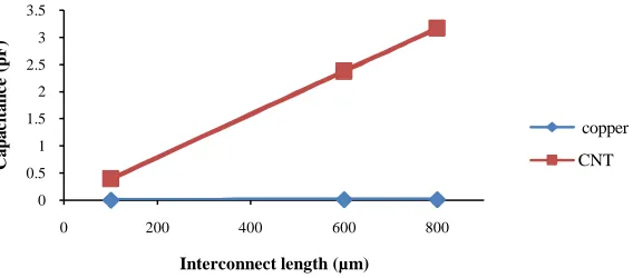
The RLC parameters of copper and SWCNT interconnect are evaluated using Eqns 1-21. Using these values obtained, the resistance, inductance and capacitance of copper and SWCNT interconnect are plotted at local, Semiglobal and global interconnect length which is shown in Fig.6-8 The values of parasitic are shown in the Table 1 for Semiglobal length of interconnect where it is clear that the resistance and inductance of copper is higher than CNT whereas the capacitance of copper is lower than SWCNT interconnect. Using these parameters the delay and power dissipation for copper and SWCNT interconnect has been evaluated with the help of Tanner EDA tool worked at 22nm technology node.
Fig 6 Comparison of resistance between Copper and SWCNT interconnect at 22nm tech node 0 500 1000 1500 2000 2500 3000 3500 4000
0 200 400 600 800 1000
R e si sta n c e ( Ω )
Interconnect length (µm)
It is very clear from the graph that the value of resistance and inductance for copper is far much more than CNT interconnect. The reason behind this is various effects like skin effect, electromigration, grain boundary effect taking place in copper that generally increases its resistance and hence leading to increase in delay. But the capacitance of CNT is more than copper, thus it contributes more in the power dissipation.
Table 1 Impedance parameter at Semiglobal length of interconnect
Parameters Copper
interconnect
SWCNT interconnect Thermally aware
resistance(300K)(Ω) 2816 353.523
Temp. independent
resistance (Ω) 2816 461.43
Capacitance (pF) 0.0106 2.3775
[image:6.612.123.490.341.494.2]Inductance (pH) 1103.95 0.098835
Fig 9 and Fig 10 shows the delay and power comparison between copper and CNT interconnect at 22nm technology node. It is very clear that the delay in copper is much more than SWCNT interconnect. This is because the resistance in copper is high than SWCNT interconnect. Thus CNT can be used in high speed applications.
Fig 7 Comparison of inductance between Copper and SWCNT interconnect at 22nm tech node
Also the power dissipation in CNT is less than copper though CNT has high capacitance. The capacitance of CNT contribute more in power dissipation, thus on varying capacitance the power can be varied as well.
Fig 8 comparison between the capacitance of Copper and SWCNT interconnect at 22nm tech node 0 200 400 600 800 1000 1200 1400 1600
0 100 200 300 400 500 600 700 800 900
In d u c ta n c e
Interconnect length (µm)
copper (pH)
CNT (fH) 0 0.5 1 1.5 2 2.5 3 3.5
0 200 400 600 800
C a p a c ita n c e (p F )
Interconnect length (µm)
copper
[image:6.612.168.452.560.685.2]Fig 9 Comparison between the delay of copper and SWCNT interconnect at 22nm tech node
[image:7.612.152.439.495.684.2]Fig 10 Comparison between the power of copper and SWCNT interconnect at 22nm tech node
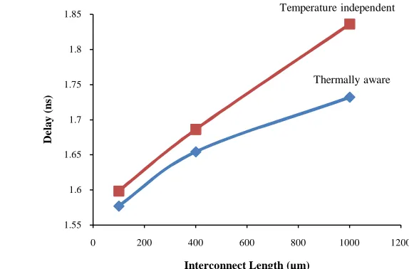
Fig 11 Comparison between the delay of SWCNT interconnect for thermally aware and temperature independent model of resistance 1 1.5 2 2.5 3 3.5 4 4.5 5
0 200 400 600 800 1000
D e la y (n s)
Interconnect Length (µm)
Copper CNT 0 0.1 0.2 0.3 0.4 0.5 0.6 0.7 0.8 0.9
0 200 400 600 800 1000 1200
P o w e r (µW )
Interconnect Length (µm)
Copper CNT 1.55 1.6 1.65 1.7 1.75 1.8 1.85
0 200 400 600 800 1000 1200
D e la y (n s)
Interconnect Length (µm)
Temperature independent
Fig 11 shows the comparison between the delay of temperature dependent and independent model of resistance for SWCNT interconnect. Thermally aware model is considered at 300K. It is very clear from the graph that the thermally aware model gives less delay than that of temperature dependent model. This is so because the resistance of temperature independent model is always higher than thermally aware model. Thus it can be easily said that copper can be replaced by CNT in interconnect application.
V. CONCLUSION
The comparison between delay and power of copper and CNT interconnect has been done for local, Semiglobal and global interconnect. The values of resistance, inductance and capacitance have also been evaluated and it is clear that with changing these parameters the delay and power can be changed. It has been observed that for any length of interconnect the delay for copper is more than SWCNT due to higher resistance. Also power dissipation in copper is much high than SWCNT interconnect. The temperature dependent delay has also been evaluated and it is clear that thermally aware delay in SWCNT is also less than temperature dependent delay. Thus, because of all these advantages CNT can be used as a future interconnect material in VLSI application.
REFERENCES
[1] Brajesh Kumar Kaushik, Saurabh Goel and Gaurav Rauthan, “Future VLSI interconnects:Optical fibre or carbon nanotube -a review”, Microelectronics international, pp. 53–63,2007 .
[2] Franz Kreupl, Andrew P. Graham, Maik Liebau, Georg S. Duesberg, Robert Seidel, Eugen Unger, “Carbon Nanotubes in Interconnect Applications,” Microelectronic Engineering, 64, pp. 399-408,2002.
[3] Jun Li', Qi Ye;Alan Cassell, Jessica Koehne, H.T. Ng, Jie Han and M. Meyyappan, "Carbon nanotube interconnects: A process solution", IEEE international. Interconnect Technology.Conference., pp. 271-272,2003.
[4] P. J. Burke, “Lüttinger liquid theory as a model of the gigahertz electrical properties of carbon nanotubes”, IEEE transactions on nanotechnology, Vol. 1, No. 3, pp 129-144, 2002.
[5] JM Rabey, “Digital integrated circuits, A design perspective”, Prentice-Hall, Englewood Cliffs, NJ,1996.
[6] Mayank Kumar Rai, Brajesh Kumar Kaushik, Sankar Sarkar, “Thermally Aware performance analysis of single walled carbon nanotube bundle as VLSI interconnect”, Springer Science + Business Media, pp 407-419,2016.
[7] Amir Hosseini, Vahid Shabro, “Thermally aware modeling and performance evaluation for single walled carbon nanotube based interconnects for future high performance integrated circuits”, Microelectronics Engineering, 87, pp. 1955-1962,2009.
[8] Kaustav Banerjee and Naveen Srivastava, “Are Carbon Nano Tubes the future of VLSI interconnections”, In:43rd ACM IEEE DAC conference proceedings,San Francisco,pp. 809-814,2006.
[9] Arijit Raychowdhury, and Kaushik roy, “Modeling of metallic carbon Nanotubes interconnects for circuit simulations and a comparison with cu Interconnects for scaled 80 technologies”, IEEE transactions on computer aided design of integrated circuits and systems, Vol. 25, No. 1, pp 58-65,2006.