Critical Path Reduction by Efficient Use of
Retiming and Its Implementation on FIR Filter of
256-Bit Length
R.Joshi1, B.K.L.Aruna2
1
M.Tech in VLSI & ES, Student at Velagapudi Ramakrishna Siddhartha Engineering College, Jawaharlal Nehru Technological University -Kakinada, Kanuru, Vijayawada-7, Andhra Pradesh
2
Assistant Professor, Electronics and Communication Engineering department, Velagapudi Ramakrishna Siddhartha Engineering College, Jawaharlal Nehru Technological University -Kakinada, Kanuru, Vijayawada-7, Andhra Pradesh
Abstract: Retiming transformation modifies the position of delay elements in a circuit without effecting its input–output characteristics of the circuit. Traditionally, the retiming based on propagation delay information can be evaluated by discrete component model. This model obeys data dependency requirement where the operation of a data flow graph node (DFG) can start after executing operation of its preceding nodes. By the technique connected component timing model, it could be easy to obtain satisfactory estimates of propagation delays on different paths in data flow graphs. This could be used for efficient retiming to reduce the critical path significantly without consequential increase in the register-complexity and the latency. The recommended technique for the deduction of critical path by combining retiming with the node-splitting and node-merging could be used at the cost of register complexity. Finally, the application of proposed technique in FIR filter of 256-bit length could be discussed.
Keywords: Retiming, Cut-set retiming, FIR filter, Data flow graph, latency
I. INTRODUCTION
Retiming transformation modifies the position of delay elements in a circuit without effecting its input–output characteristics [1]. It has several applications in the design and optimization of synchronous circuits. This technique has no of applications in designing and optimization of circuits e.g. clock period is reduced, total number of registers used in circuit can be reduced, required power to run the circuit can be decreased [1]-[4]. The technique used for dividing a normal data flow graph into sub graphs can be called Cutset Retiming. This can be implemented by changing the position of certain no of delays to or from incoming and outgoing edges of the sub graphs. This can be effectively used in architectural level of designing a digital system for deduction of period of clock. In present days, the retiming problem can be solved by assuming the propagation delays on various paths are to known [1] - [5]. Traditionally, based on propagation delay information the retiming can be evaluated by the model called Discrete Component Model. This model obeys data dependency requirement where the operation of a Data Flow Graph (DFG) node can start after executing operation of its preceding nodes. It has been shown that this model gives higher approximation of propagation delays than existing, and results unwanted grow in pipeline overhead in terms of register complexity and latency [6],[7]. Let us illustrate this case by two simple examples in the following
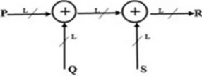
Fig. 1 (a) Multiply–addition circuit to compute R = P × Q + S.
[image:2.612.232.375.661.715.2]It is clearly understood that word-length is not affected by the addition. Anyway, the word-length should increase by 1-bit after the additions.
The DFG in Fig. 1(a) represents the estimation of R = P×Q+S and the DFG in Fig. 1(b) means the estimation of R = P + Q + S. The word-length of each of P, Q, and S is L. Traditionally, propagation delays of the circuits in Fig. 1(a) and (b) are
TMA = TMULT + TADD (1.a) TADD = 2TADD (1.b)
Where TMULT and TADD are, the times required for a multiplication and an addition respectively. The conventional estimate of propagation delay assumes the adders and multipliers as discrete components, where the operation of one circuit can start after executing whole operation of other circuits. The intermediate signals produced during the computation pass uniformly across the combinational data-path, thus an operation can start as soon as the first output of its preceding operations and other input are present and no need to wait for the whole of the preceding operations to be performed. The current propagation delays of the circuits in Fig. 1(a) and (b) are much less than these conventional valuations. It can be easily found that TMA is much less than TMULT + TADD. The computation time for adder of operand circuit (T3OP-ADD) is ample less than 2TADD and the computation time for adder of three-operand circuit (T4OP-ADD) is ample less than 3TADD. The following may explain this behavior of circuits in Fig. 2.
Fig. 2 (a) Multiply-add circuit. RCA: ripple carry adder
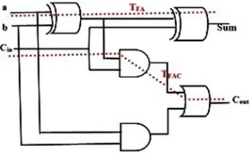
Fig. 2(a) shows a multiply–addition circuit for the computation of P × Q + S, here each of P and Q is a 4-bit word and S is an 8-bit word. The product T = P × Q is an 8-bit word. From this figure, we can find that after the product T is calculated by the multiplier unit, for the addition of T with S, a 2-bit addition is necessarily to be performed to finish the multiply–addition operation. The propagation delay of the multiply–addition circuit is given by
TMA = TMULT+TFA+TFAC (2a)
Where, TFA is the propagation delay of a one-bit full-adder (FA). TFAC is the time required by an FA to generate the output carry after the arrival of the input carry if the other two input bits are available to the FA in advance (appears as dashed lines in Fig. 3). Anyway, the bit length may increase by 1 bit after the addition and this can be given as
TMA = TMULT + TFA + 2TFAC (2b)
[image:3.612.204.408.279.424.2] [image:3.612.213.398.603.706.2]Fig. 3 Propagation delays TFA and TFAC in a 1-bit FA.
Fig. 2(b) shows the result of three-operand addition R = P + Q + S, where each of P, Q, and S is an 8-bit word. Let us consider, increase in bit-width does not take place due to this addition, then sum word T = P + Q and R are also 8-bit words. From this figure, we can find that after the sum T is calculated by the first adder, the addition of T with S needs 1-bit FA time, TFA. Consequently, the propagation delay of the three-operand additions of the form R = P + Q + S, is stated by
TAA = TADD + TFA (3a) Anyhow, if we consider the increase in bit-width after the addition, we can obtain it to be
TAA = TADD + TFA + TFAC (3b)
The timing model used in the propagation delay evaluation of Eq.1 is described as the discrete component timing model, while that of Eq.2 and Eq.3 is represented the connected component timing model. Let us consider the gate level description of digital circuits, then the precise estimate of propagation delay could be provided by discrete component timing model. Yet very often it is essential to deal with the DFGs at the granularity of arithmetic operators for mapping an algorithm to desired architecture at the architecture-level abstraction of the digital system design, here the discrete component timing model gives overestimates of propagation delays and leading to undesirable pipelining. We can easily obtain satisfactory precise estimates of propagation delays on different paths in a DFG by connected component timing model, and can use that for efficient retiming to reduce the critical path significantly without consequential increase in the register-complexity and the latency. From this paper the main contributions are as follows.
A. It expresses that the architecture level traditional retiming (based on discrete component timing model) doesn’t lead to effective reduction in critical path or the minimum sampling period (MSP), but leads to undesirable pipelining and unwanted increase in pipeline overhead. Moreover, based on connected component timing model it introduces preferable alternative retiming.
B. To achieve significant reduction in critical path, some nodes of the DFG could be split and some could be merged before and after the retiming. It illustrates the use of splitting and merging of nodes for efficient retiming of some popular digital signal processing (DSP) circuits, e.g., finite impulse response (FIR) filters.
II. RETIMING AND ANALYSIS
The limitation of usually used traditional retiming of FIR filter and propose a low-overhead possible retiming based on connected component timing model. Beyond the two-slow transformation of lattice filters does not assist minimize the MSP but enlarge the power consumption.
A. Connected Component Timing Model
B. Retiming of FIR Filter
The limitation of conventional retiming of direct-form (DF) FIR filter is discussed and a flexible retiming (FX-R) scheme based on precise estimation of propagation delay derived from the connected component timing model is proposed. Corresponding to the throughput requirement of the given application, the FX-R allows to select the cut sets where register complexity can be traded for performance.
1) Limitations of Conventional Retiming of FIR Filter: The DFG of the DF FIR filter of length N = 8 is given in Fig. 4(a). Depending on the delay model given in Eq.2 and Eq.3, let us assume that the output adder-chain could be implemented by a binary adder-tree then the critical path of an FIR filter of length N can be evaluated as
TDF = TMULT + ┌ log2 N ┐α (4a)
Where, α = TFA+TFAC (4b)
Fig. 4 (a) DFG of FIR filter of length N =8
Fig. 4(b) Decomposition of DFG to two sub graphs G1 and G2 for feed-forward cut set retiming of DFG
Fig. 4(c) Retimed DFG
To decompose the DFG into two sub graphs G1 and G2 as shown in Fig 4(b), the dashed line in Fig 4(a) moves by covering a feed-forward cut set [1]. By adding a delay element on all the edges going from sub graph G1 to sub graph G2 the Retimed DFG {Fig. 4(c)}. Let us consider that the input samples and coefficients to be of L-bit words, and then the product word to be of 2L-bits. Furthermore, the addition time of 2L-bit words could be related with that of the L-bit multiplication time. Hence, the critical path of DF retimed (DF-R) FIR filter {Fig. 4(c)} could be estimated by the time required by the final adder, and can be given by
TDF-R = TADD + (┌ log2 N ┐) − 1) α + TD-FF (5)
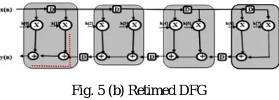
[image:5.612.41.561.92.434.2] [image:5.612.218.394.345.433.2]2) Flexible Retiming of FIR Filter Based on Connected Component Timing Model: A workable design for the retiming of DFG of Fig 4(a), to implement the required retiming, the accumulation path direction is reversed in the DFG (as represented in Fig 5(a)), and the cut sets over the dashed lines (following every gray box) are examine one after the other for the retiming. The edges of a cut set are removed during each of those retiming’s to decompose the DFG into pairs of sub graphs, and finally to get retimed DFG the delay on the upper edge of the sub graph is shifted to the lower edge as appear in Fig 5(b). The critical path of this retimed DFG is represented in dashed line.
Fig. 5 (a) Cut set selection for the proposed retiming of DFG of the FIR filter of length N =8
Fig. 5 (b) Retimed DFG
The critical path of retimed DFG by depending on the delay model of Eq.2 and Eq.3 can be represented as TFX-R = TMULT + 2TFA +
(┌ log2 N ┐) + 1) TFAC + TD-FF (6)
It is also possible to consider cutsets after four multiply add sections or after eight or after 16 sections to decrease register complexity at the cost of small rise in critical path by TFA or 2TFA or 3TFA individually. Hence the number of registers could be trade easily for critical path by suggested technique of retiming [8].
a) From Eq.5 and Eq.6 we can observe that the conventional retiming of DFG has lower critical path for small filter lengths and for higher filter lengths the suggested retiming of fig.5 involves lower critical path
b) The conventional retimed DFG requires N extra registers of 2L bit size , at the same time the suggested one allows only NL additional registers
c) So in the suggested technique the critical path can be easily traded for register complexity and vice versa
d) The two-slow transformation requires two clock cycles to produce each output sample and has no advantage over direct retiming but also consumes nearly twice the energy per output sample compared with suggested technique
III. EFFICIENT RETIMING
This portion discuss the suggested technique [8] for the scaling down of critical path using combination of retiming with splitting of nodes and merging of nodes. Apart from this the application of the suggested method in FIR filter is discussed.
A. Splitting and Merging of DFG Nodes
It is very easy to split an adder circuit into two almost equal parts as shown in Fig.6 for the ripple carry adder (RCA) to compute the addition T = P + Q, here P and Q are of 8-bit words.
[image:6.612.207.406.255.327.2]Similar splitting can be executed for carry-look ahead adders also. From the reference paper Seamless pipelining of DSP circuits [6], they showed that it is very easy to decaying a Wallace-tree Multiplier into two parts there each section includes almost half of the propagation delay of a multiplier, for fine-grained seamless pipelining of multiplier and multiply–add circuits. Such a circuit is given in Fig.7 for the division of a multiplier for the execution of T = P × Q, here P and Q are of 8-bit words.
Fig. 7 Splitting multiplier Circuit
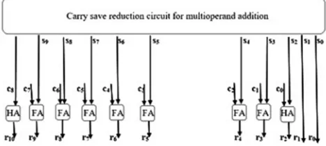
Whenever it is required to add a large number of words, it uses a carry-save reduction (CSR) section part. By a CSR section part, M operands can be deduced to a pair of words by x scaling down stages, it satisfies the condition ┌ M (2/3) x┐= 2. It is quite simple to test that x = 2 (log2 M − 1) for M = 4, 8, 16, 32, 64, etc. Every CSR stage has only 1-bit FA delay, TFA. The carry and the sum words produced by the CSR section part can be summed together by a final adder. As given in [7], it is easy to divide multioperand adder into two parts having nearly same propagation delays for pipeline Implementation. This type of circuit is shown in Fig.8 for the addition of 8 number of 8-bit words.
Fig. 8 Splitting of multioperand adder
B. Retiming of an FIR Filter combined with Splitting and Merging of Nodes
This part explains about the scaling down of critical path of FIR filter through splitting and merging of nodes together with retiming method. The DFG of FIR filter of length N = 4 is presented in Fig. 9(a) here the multiplication nodes and addition nodes are divided into two parts of nearly equal delays.
[image:7.612.187.421.390.495.2]The feed-forward cutset is represented by the horizontal dotted line in Fig. 9(a); and the following retimed DFG is presented in Fig.9 (b).
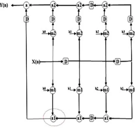
Fig. 9(b) Splitting of nodes of the DFG
Two pairs of [m1, a1] connected nodes in the DFG of Fig. 9(b) could be merged to create nodes N1 and N2. In order to obtain the final DFG of Fig.10, the DFG of Fig. 9(b) can be node-retimed around the last a1 node. The node N3 can be formed by merging the last a1 node, chain of two a2 nodes, and the final adder node a and it could be executed by a four-operand adder. Assume that the multiplication nodes and adder nodes are divided into two parts of almost equal propagation delay of 1 u.t, where 1 u.t = (1/2) TMULT or (1/2) TADD, here TADD is (∼2L)-bit addition time, while TMULT is the time needed for multiplication of two L-bit words, the
propagation delay of N1 and N2 nodes can be nearly 1 + α .
The critical path of the retimed FIR filter is almost equals to the delay of N3 node, it amounts to TFIR-RT = ∼ (1/2) TMULT + 3 α (7)
[image:8.612.188.420.121.342.2]Where α is explained in (4b). Since α is less compared to TMULT, the suggested retiming combined with splitting and node-merging can evolve in considerable deduction of the critical path over the lowest achievable critical path by the standard retiming.
Fig. 10 Feed-forward cutset retimed DFG of Fig. 9
C. Synthesis Results and Discussions
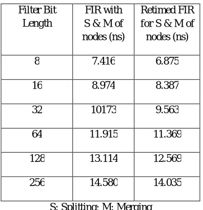
[image:8.612.201.430.535.648.2]respective filter bit lengths. Similarly, the Table II consists of node splitting and merging for FIR filter along with proposed technique of retiming
. Filter Bit Length FIR filter (ns) Retimed FIR (ns) Cutset Retimed FIR (ns)
8 13.720 8.454 5.009
16 23.760 9.654 6.209
32 43.533 11.556 8.112
64 81.104 12.733 9.288
128 154.399 14.199 10. 754
[image:9.612.208.406.333.538.2]256 300.906 15.375 11.930
Table I: combinational path delay of FIR for the proposed technique
Filter Bit Length
FIR with S & M of nodes (ns)
Retimed FIR for S & M of nodes (ns)
8 7.416 6.875
16 8.974 8.387
32 10173 9.563
64 11.915 11.369
128 13.114 12.569
256 14.580 14.035
S: Splitting; M: Merging
Table II: combinational path delay of FIR with S and M of nodes
IV. CONCLUSION
The proposed techniques can be helpful for less pipeline overheads as exact estimation of propagation delays can be made by connected component model, which results easy way to obtain exact estimation of propagation delays over different paths in DFG. The advantage of proposed retiming technique is critical path reduction, later it shown that the splitting and merging of nodes may results less combination path delays. This techniques of fixed point circuits can be extended to floating point circuits. These methods could be useful in digital signal processing and FIR, IIR filters.
REFERENCES
[1] K. K. Parhi, VLSI Digital Signal Processing Systems: Design and Implementation. NewYork, NY, USA: Wiley, 200 [2] C. E. Leiserson and J. B. Saxe, “Retiming synchronous circuitry,” Algorithmica, vol. 6, nos. 1–6, pp. 5–35, Jun. 1991.
[3] L.-F. Chao and E. H.-M. Sha, “Scheduling data-flow graphs via retiming and unfolding”, IEEE Trans. Parallel Distrib. Syst., vol. 8, no. 12, pp. 1259–1267, Dec. 1997.
[6] P. K. Meher, “Seamless pipelining of DSP circuits,” J. Circuits Syst. Signal Process, Jul. 2015. [Online]. Available: http://link.springer.com/article/10.1007%2Fs00034-015-0089-2
[7] P. K. Meher and S. Y. Park, “Critical-path analysis and low-complexity implementation of the LMS adaptive algorithm,” IEEE Trans. Circuits Syst. I, Reg. Papers, vol. 61, no. 3, pp.778–788, Mar. 2014.
[8] On Efficient Retiming of Fixed-Point Circuits Pramod Kumar Meher, Senior Member, IEEE, IEEE transactions on very large scale integration (vlsi) systems, vol. 24, no. 4, april 2016