International Journal of Emerging Technology and Advanced Engineering
Website: www.ijetae.com (ISSN 2250-2459,ISO 9001:2008 Certified Journal, Volume 4, Issue 8, August 2014)
251
Design of Optical Demultiplexer using Arrayed Waveguide
Grating
Sukhjeet Kaur
1, Dr. Amandeep Singh Sappal
21
Student, 2Assistant Professor, Department of Electronics and Communication Engineering, Punjabi University, Patiala Abstract-- Optical demultiplexers are used to receive
multiple frequency signal from an optical fiber and to split it into its different frequency components. Arrayed waveguide gratings can be used to design an optical demultiplexer and works on the principle of interferometry. This paper presents the design of optical demultiplexer for an optical signal composed of eight frequency components. Simulation results have been presented.
Keywords
--
Arrayed Waveguide Grating, Demultiplexer, Interferometery, Optical Spectrum, Photonics.I. INTRODUCTION
The foremost function of an optical demultiplexer is to receive a beam comprised of multiple optical frequencies from a fiber and to divide it into its frequency components, which are further coupled in as many individual fibers as there are frequencies. Optical multiplexer functions exactly in the reverse manner. It receives number of optical wavelengths from many fibers and congregates them into one beam that could be coupled into a single fiber[1]. These are divided into two categories, passive and active devices. First one are based on prisms, diffraction gratings, and frequency filters and next are, Active demultiplexers are based on a arrangement of passive components and tunable detectors, every detector tuned to a specific frequency. Arrayed waveguide gratings (AWGs) works on the principle of interferometry. To explain the working of AWG, consider a fiber carrying a multiplicity of wavelengths λ1, λ 2… λ N. The light of all wavelengths from fiber shine in cavity S1 and the same is coupled to an array of waveguides, W1 to WN ' . The optical length
difference of every waveguide introduces wavelength- dependent phase delays in cavity S2 to which an array of fibers is coupled[2]. Due to the change in length of fibers phase difference of each wavelength gets hinder in such a way that each wavelength contributes maximally at every end of the output fibers.
Figure: 1 Working principle of AWG
Some typical characteristics of AWG are as follows:
AWGs are polarization dependent, but means to overcome this enslavement have been reported.
AWGs are temperature sensitive.
The preferred operating range of temperature (0°-85°C).
AWGs provide good flat spectral response accordingly eases in wavelength control.
Insertion loss is in the under -3-dB range.
and cross-talk level is better than -35 dB.
AWGs are more suitable for integration with photodetectors [1].
II. DEMULTIPLEXER DESIGN
International Journal of Emerging Technology and Advanced Engineering
Website: www.ijetae.com (ISSN 2250-2459,ISO 9001:2008 Certified Journal, Volume 4, Issue 8, August 2014)
252
The central propagation constant, the modal half-width and the difference in propagation constant of the two polarizations BTE and BTM are fixed as according to thechoice of the waveguide geometry. The demultiplexer could be made polarization independent by selecting the parameters. Afterword with a lateral receiver-waveguide spacing d = 5 pm and a comparative- channel spacing, the focal length becomes 123 pm. The channel crosstalk considerations are similar to the polarization splitter design explained in [3]. A receiver-waveguide spacing of 5 pm and a number Np = 3 1 array waveguide shall be sufficient for a channel segregation better than -45 dB. When the fan-in and fan-out section length t is selected at least equal to the focal length, the mutual coupling between adjacent waveguides would become negligible. Though the concentric sector angle P, is so chosen thatthe phased array can perform a wavelength-demultiplexing function. Demultiplexer was consequently designed for TE polarization. The polarization-independence was achieved by adjusting the focal length according to specifications. To average the demultiplexer performances for both polarizations, the deviation correction shall be averaged, so that the receiver waveguides are placed such a manner that the focal mismatch is same for both polarizations. These correction are not implemented for the present design. Even better solution could be obtained to an aberration-free design. To examine the feasibility of such a design is presently being performed. The theoretical performance of this design could be computed by same transmitted signal through the demultiplexer as explained in [3]. The field at the input plane of the array is considered as the two-dimensional diffraction field of the fundamental- mode outline at the end of the transmitter waveguide.
III. SIMULATION RESULTS
This paper proposes a type of Arrayed Waveguide Grating, the method used in configuration based on phase shifters and Sagnac Loop Reflectors, usually build with an optical coupler with looped back waveguides. A model for the design and analysis of the device have been provided, for both the cases of Gaussian and flattened response, the second achieved by adjusting the AW field distribution to a sinc function by use of the single lens reflex and phase shifters. The model has been used to design and simulate Silicon-on-Insulator implementations via typical waveguide cross-sections for the technology.
[image:2.612.323.564.219.347.2]The work is presented for both the Gaussian and flattened spectral response, where as for different field distributions in the AWG arms which will result in principle with an arbitrarily customizable spectral response.
Table 1
Transmitted and received optical power for different frequencies.
Channel Frequency
in THz
Power Tx Power Rx
1 193 -3.0526 -5.0859
2 193.1 -4.6016 -4.5496
3 193.2 -3.1356 -5.1913
4 193.3 -2.7045 -4.2585
5 193.4 -2.7524 -5.3670
6 193.5 -2.3662 -4.2068
7 193.6 -2.4781 -3.0912
8 193.7 -2.6351 -4.9750
[image:2.612.337.535.447.637.2]International Journal of Emerging Technology and Advanced Engineering
Website: www.ijetae.com (ISSN 2250-2459,ISO 9001:2008 Certified Journal, Volume 4, Issue 8, August 2014)
International Journal of Emerging Technology and Advanced Engineering
Website: www.ijetae.com (ISSN 2250-2459,ISO 9001:2008 Certified Journal, Volume 4, Issue 8, August 2014)
254
International Journal of Emerging Technology and Advanced Engineering
Website: www.ijetae.com (ISSN 2250-2459,ISO 9001:2008 Certified Journal, Volume 4, Issue 8, August 2014)
International Journal of Emerging Technology and Advanced Engineering
Website: www.ijetae.com (ISSN 2250-2459,ISO 9001:2008 Certified Journal, Volume 4, Issue 8, August 2014)
256
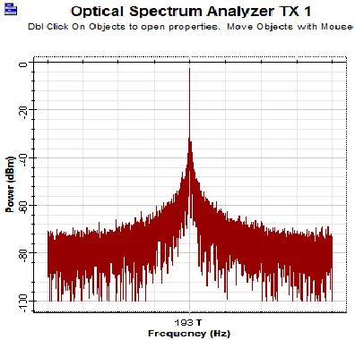
Figure:3 Graphs representing Optical spectral analyzer Receivers for 1:8 demux
Graphs have been plotted between Power and frequency for both the Transmitter and Receivers the system here used ideal multiplexer and AWG demultiplexer. It has been observed that for same frequency power is shifted with a particular level as graphs are observed.
IV. CONCLUSION
To receive multiple frequency signal from an optical fiber optical demultiplexer is used and to split received optical signal into its different frequency components, Arrayed Waveguide Gratings (AWG) can be used to design an optical demultiplexer and works on the principle of interferometry. In this paper the design of optical demultiplexer for an optical signal where the optical signal of different eight frequency components is used for experimental work. Simulation results have been presented for all the different eight frequency components.
REFERENCES
[1] G. T. Reed and A. P. Knights, “Silicon Photonics: An Introduction”. Chichester, U.K. Wiley, 2004.
[2] L. Pavesi and D. J. Lockwood, Eds.,” Silicon Photonics”. Berlin, Germany: Springer-Verlag, 2004.
[3] N. S. Patel, K. L. Hall, and K. A. Raushenbach, “40 Gbits cascadable all-optical logic with an ultrafast nonlinear interferometer”, Opt. Lett., 21, pp. 1466-1468, 1996.
[4] S. A. Hamilton, B. S. Robinson, T. E. Murphy, S. J. Savage, and E. P. Ippen, "100 Gb/s Optical time-division multiplexed networks", J. Light. Techno., 20 (12), pp. 2086-2100, Dec. 2002.
[5] C. Dragone, “An NxN optical multiplexer using a planar arrangement of two star couplers,” IEEE Photon. Technol. Lett. 3(9), 1041–1135 (1991).
[6] C. Dragone, C.A. Edwards, and R.C. Kistler, “Integrated optics NxN multiplexer on silicon,” IEEE Photon. Technol. Lett. 3(10), 896–899 (1991).
[7] T. Suhara, H. Nishihara, J. Koyama, J. Viljanen, and M. Leppihalme, “Integrated-optic wavelength multi- and demultiplexers using a chirped grating and an ion-exchanged waveguide,” in Proc. ECIO. (London, England), Sept. 1981, pp. 12-14.