HEWLETT ' " PACKARD
warranty Statement
Hewlett-Packard products are warranted against defects in materials and workmanship. For Hewlett-Packard Desktop Computer Division products sold in the U.S.A. and Canada, this warranty applies for ninety (90) days from date of delivery. * Hewlett-Packard will, at its option, repair or replace equipment which proves to be defective during the warranty period. This warranty includes labor, parts, and surface travel costs, if any. Equipment returned to Hewlett-Packard for repair must be shipped freight prepaid. Repairs necessitated by misuse of the equipment, or by hardware, software, or interfacing not provided by Hewlett-Packard are not covered by this warranty.
NO OTHER WARRANTY IS EXPRESSED OR IMPLIED, INCLUDING, BUT NOT LIMITED TO, THE IMPLIED WARRANTIES OF MERCHANTABILITY AND FITNESS FOR A PARTICULAR PURPOSE. HEWLETT-PACKARD SHALL NOT BE LIABLE FOR CONSEQUENTIAL DAMAGES.
98036A Serial
1/0 Interface
Installation and Service Manual
Hewlett-Packard Desktop Computer Division 3404 East Harmony Road, Fort Collins, Colorado 80525
ii
Table of Contents
Chapter 1 : General Information
Introduction ... 1
Background On Data Communications ... 1
98036A Description ... 3
Specifications ... 3
Cable Options ... 3
Chapter 2: Installation Introduction ... , . , ... , ... 7
Interface Housing Disassembly ... 7
Interface Configuration Switches ... 9
Factory Switch Settings ... 10
Mode Word Switches ... 10
Input/Output Mode Switch ... 12
RS-232 Driver Switch ... , ... 12
Internal/External Clock Switches ... 12
Clear To Send Switch ... 13
Bit Rate Switch ... , ... , ... , ... 13
I nterface Select Code ... 13
Interface Installation ... 14
Recommended Circuits ... , ... 14
Chapter 3: Operation Introduction ... 15
I nterface Control ... , ... 15
Bit Position Values· ... 15
R5 Registers ... , , ... , ... , ... 16
R5 OUT Register ... , ... 16
R5 I N Register ... , ... ,." ... 18
R4 Registers ... , , ... , ... , ... 18
R4A Data Output ... , 18
R4B Data Input ... , ... , .... , ... 18
R4C Mode Word· .... , , , . , , , , , , ... , .. , . , . , , , , , , .... , , .. , ... , . , ... , 19
R4D USART Control Word .... , , .... , .. , , . , ... , , ... , . , , . , ... , .. , , . , ... , 20
iii
R6 Registers ... 22
R6 OUT Register (Standard Cable) ... 22
R61N Register (Standard Cable) ... 23
R6 OUT Register (Option 001 Cable) ... 23
R6 I N Register (Option 001 Cable) ... 24
9825A/98036A Operation ... 25
Examples ., ... 25
Chapter 4: Theory of Operation Introduction ... 31
Interface Registers ... 31
Register Control ... 32
Flag Circuits ... 32
I nterrupt Circuits ... 33
Clock Generator ... 33
1/0 Drivers-Receivers ... 33
Setting Registers ... 34
Transmitting Data ... 35
Receiving Data ... 35
Reset ... , ... , ... 36
The USART ... 36
Chapter 5: Troubleshooting and Repair Introduction ... 41
Recommended Equipment ... 41
Test P.rogram ... 41
Troubleshooting ... 45
Broken Trace Repair ... 45
iv
Figures
Modem Conversion Process ... 1
I nterface Disassembly ... 8
Interface Configuration Switches ... 8
Current Loop Operation ... 14
Register Summary ... 29
Resister Access ... 29
98036A Block Diagram ... 30
USART Block Diagram ... 36
98036A Timing Diagram ... 37
Component Locators ... 38
98036A Interface Schematic ... 39
Test Connector Installed ... 42
Test Prog ram Flowchart ... 44
I nterface Test Setup ... 45
Tables Cable Signals ... 5
9825A/98036A Statements ... 25
Cable Wiring ... 40
Chapter 1
General Information
Introduction
This manual describes the installation and operation of the 98036A Serial 110 Interface when used with a 9825A Calculator and a data communications device. Theory of operation and troubleshooting chapters are also included to provide servicing information.
Background on Data Communications
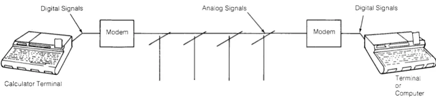
Data Communications is the means by which data is transmitted from one point to another. A
computer can be hooked directly to a remote terminal using special transmission lines, but for
long distances, this becomes impractical. Although common telephone lines can be used, there is one drawback: telephone lines are made for analog signals (e.g., the voice), not digital
signals like those generated by a computer. A modem*,or a signal converter, must be used for
converting signals from digital to analog and vice-versa.
Digital Signals Analog Signals
Calculator Terminal
Figure 1. Modem Conversion Process
Digital Signals
Terminal or Computer
The modem converts outgoing digital signals to analog form and incoming analog signals to
digital form (Figure 1). Since there are many different ways to do these conversions, it is
important that what is converted to analog is reconverted to the correct digital form and
vice-versa. So, the modem on one end of the telephone line must understand, or be
compati-ble with, the modem on the other end.
Modems can be classified as asynchronous or synchronous, half- or full-duplex, and by data
rate or modulation technique.
[image:7.613.110.535.464.559.2]2 General Information
Asynchronous transmission is often referred to as START-STOP. This is because the data is
sent serially one character at a time along with start and stop bits. These start and stop bits are used to separate characters and to synch ronize the receiver with the transmitter for each
character since the modem itself does not provide clocking information. When the signal
elements or bits of a character travel in sequence over the line, it is called a serial
transmis-sion. With the start and stop bits added, this is called serial start-stop or serial asynchronous,
meaning each character is individually synchronized. This type of transmission is normally
used at data rates less than 2400 bits per second.
Parity Bit
Start Bit Data Bits Stop Bits (Optional)
Asynchronous Mode Transmission
Modems can operate in three different modes: simplex, where data is sent only or received
only; half-duplex, where data can be both sent and received - but not simultaneously; and
full-duplex, where data can be simultaneously transmitted and received, eliminating
turn-around time.
Half-duplex is normally used for high speed batch transmission where fewer line
turn-arounds are needed and full channel capacity (bandwidth) is needed for transmission in
one direction. Full-duplex is often used for timesharing even though it seldom occurs that
data is truly being transmitted and received simultaneously. The one case were simultaneous
transmission does occur is when a "Break" is sent to the timeshare computer. A single dial-up
line can be used for fu"-duplex but this limits the maximum data rate to about 300 bits per
second. The reason for full- duplex timesharing is to provide transmission error checking by
having the computer "echo" or retransmit each character input from the terminal.
The most commonly referenced operational characteristic of a modem is its speed or data rate
expressed in bits per second (bps) or bauds. For simple low speed modulation techniques, one bit per second into a modem may equal one baud on the analog side. However, at higher
data rates with more complex modulation techniques, it is possible to encode more than one
bit per signal change (or baud) on the telephone line. In this case, bits per second (into the modem) and bauds (on the telephone line) are two different units. The following list gives a
general classification of modems by speed:
Low Speed 75 -1800 bits/second
Medium Speed 2000-4800 bits/second
General Information 3
98036A Description
The HP 98036A Serial I/O Interface allows the 9825A Calculator to communicate with serial asynchronous data communication devices. The 98036A is equipped with both RS-232C and 20ma current loop drivers and receivers for the data transmitter and receiver. Data can be transferred at bit rates of 75 to 9600 bits per second. The interface is capable of asynchronous communication. A universal receiver/transmitter integrated circuit (USART) is used to manipu-late data and provide the basic hardware protocol for asynchronous operation. Either the General I/O ROM or the General and Extended I/O ROM combination must be installed in the calculator to use the interface. The interface is available with two cable configurations to allow the calculator to act as a data terminal or the digital portion of a modem*.
Specifications
Power Requirements: +5V at 300ma typo 400 max. (from calculator) ± 12V at 20ma typo 40 max.
Operating Temperature Range: 0° C to 45° C
Bit Rates: 9600, 4800, 2400, 1800, 1200, 600, 300, 150, 110, and 75 bits per second.
Mode of Operation: Asynchronous
Data Buffer: Transmitter-one character Receiver-one character
Dimensions: Approximately 16.3 x 8.9 x 3.8cm (6.4 x 3.5 x 1.5 inches) Net Weight: 4.16 kg (I lb. 14 oz.)
Cable Length: 2 meters (6.5 ft)
Cable Options
The 98036A Interface is available in two configurations.
The standard 98036A Interface cable is shipped with a 2 meter (6.5 ft.) cable terminated with a standard female EIA 25 pin connector. The standard interface is connected between the calculator and data terminal.
4 General Information
Standard Cable Connector
Using the standard interface cable, the calculator takes the place of a modem or computer
communicating with a terminal.
98036A
ModeM
r---t\
Teemice' IData Channel
I---i Terminal
Calculator
Using Normal Data Communications Using 9825A/98036A (Standard)
The 98036A Option 001 Interface cable is shipped with a 2 meter (6.5 ft.)cable terminated with
a standard male EIA 25 pin connector. The option 001 interface is connected between the
calculator and a modem.
Option 001 Cable Connector
Data
Channe, L...--MOd----Jem
1---11
T oem;,.' I DataChannel
General Information 5
98036A Mod em 1--_----1
Calculator
Using Normal Data Communications Using 9825A/98036A (Option 001)
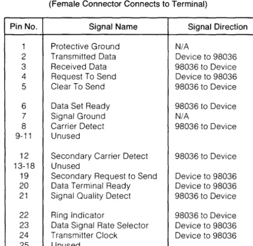
Here is a list of the signal lines and the corresponding connector pin numbers used in the standard and option 001 cables.
Table 1. Cable Signals
98036 Standard Cable
(Female Connector Connects to Terminal)
Pin No. Signal Name Signal Direction
1 Protective Ground N/A
2 Transmitted Data Device to 98036 3 Received Data 98036 to Device 4 Request To Send Device to 98036 5 Clear To Send 98036 to Device
6 Data Set Ready 98036 to Device
7 Signal Ground N/A
8 Carrier Detect 98036 to Device 9-11 Unused
12 Secondary Carrier Detect 98036 to Device 13-18 Unused
19 Secondary Request to Send Device to 98036 20 Data Terminal Ready Device to 98036 21 Signal Quality Detect 98036 to Device
[image:11.620.197.444.287.527.2]6 General Information
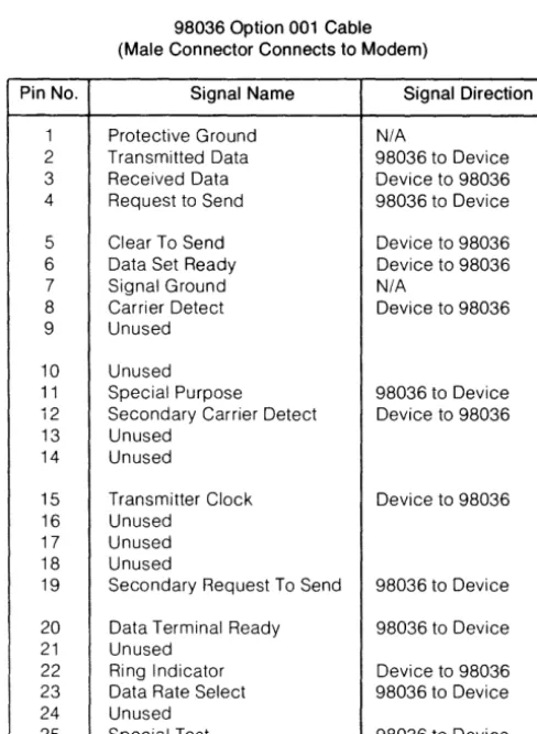
Table 1. Cable Signals (cont.)
98036 Option 001 Cable (Male Connector Connects to Modem)
Pin No. Signal Name Signal Direction
1 Protective Ground N/A
2 Transmitted Data 98036 to Device 3 Received Data Oevice to 98036 4 Request to Send 98036 to Device
5 Clear To Send Device to 98036 6 Data Set Ready Device to 98036 7 Signal Ground N/A
8 Carrier Detect Device to 98036 9 Unused
10 Unused
11 Special Purpose 98036 to Device 12 Secondary Carrier Detect Device to 98036 13 Unused
14 Unused
15 Transmitter Clock Device to 98036 16 Unused
17 Unused 18 Unused
19 Secondary Request To Send 98036 to Device
20 Data Terminal Ready 98036 to Device 21 Unused
22 Ring Indicator Device to 98036 23 Data Rate Select 98036 to Device 24 Unused
[image:12.623.173.417.121.455.2]Introduction
Chapter 2
Installation
Before installing the interface in your system it will be necessary to configure the interface for your particular system or mode of operation. This chapter describes how to configure and install the 98036A Interface. The interface switches set the power-on default condition of the interface. This default condition is used when power is applied or the calculator is reset.
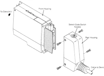
Interface Housing Disassembly
To access the various interface configuration switches it is necessary to separate the interface housing cases. Use the procedure below and refer to Figure 2 to access the switches.
1. Remove the four screws that hold the rear housing to the front housing.
2. Pull the rear housing off the front housing slightly, disconnect the cable connector from the PC assembly and remove the rear housing.
3. Remove the remaining four screws in the front housing and separate the front housing cases.
4. Carefully separate the printed circuit assemblies.
5. The various interface switches are shown in Figure 3.
6. After setting the switches, reverse this procedure to assemble the interface. Be sure that the pins on the A2 assembly are properly seated in the connectors on the A 1 assembly.
8 Installation
To Calculat:y
,
~Front Housing
Select-Code Switch Access
[image:14.613.112.481.89.633.2]Figure 2. Interface Disassembly
Figure 3. Interface Configuration Switches
UP Current Loop
[image:14.613.112.465.111.370.2]Current Loop
Factory Switch Setting
[image:15.615.102.555.59.437.2]External External
Figure 3. (cont.)
Always High
Default Mode Word Switch
Interface Configuration Switches
Installation 9
The following presentation describes how to set each of the interface configuration switches.
The questions below will help you determine how the interface switches should be set.
• What select code will you use?
• What is the bit rate?
• Will operation be RS-232 or current loop?
• Will the internal clock be used for the transmitter and receiver clock?
• Does your data communications device provide the clear to send line (option 001 cable)?
10 Installation
• What is the bit length of the characters to be transferred?
• Will parity be used?
• Even or odd parity?
• How many stop bits will be used?
• What bit rate factor will be used?
Factory Switch Settings
The interface configuration switches are preset at the factory as follows:
• Select code (Standard cable) - 10
• Select code (Option 001 cable) - 11
• Bit rate - 300 bits/second
• RS-232 operation selected
• Internal transmitter and receiver clock used
• Clear to send line is pulled up
• Character length set to 8 bits
• Parity is disabled
• 2 stop bits are selected
• The bit rate factor is 1/64
Mode Word Switches
The mode word switches (see Figure 3) determine the default mode word used by the
inter-face. The mode word determines the mode of interface operation. The default mode word is
used when power is applied to the interface or when the interface is reset. The default mode
Installation 11
1 Position
BIT 7 I BIT 6 BIT 5 BIT 4 BIT 3
I
BIT 2 BIT 1 I BIT 0Number of Stop Bits Charact~r Length Bit Rate Fa~tor
00 = not valid Parity Type Parity Enable 00 = 5 bits 00 = not used
01 = 1 bit 0= Odd 0= Disable 01 = 6 bits 01 = 1 \ bit rate clock
10= 1.5 bits 1 = Even 1 = Enable 10=7bits 10 = 1/16 X bit rate clock
11 = 2 bits 11 = 8 bits 11 = 1/64 X bit rate clock
Any switch set to the open position sets the switch to a logical 1 (high). Any switch set to the opposite position sets the switch to a logical 0 (low).
• Bits 7 and 6 - Determine the number of stop bits used.
• Bit 5 - Determines whether odd or even parity is to be used (when parity is enabled).
• Bit 4 - Enables or disables parity
• Bits 3 and 2 - Indicate the length of the characters that are to be transferred.
• Bits 1 and 0 - Determine the internal bit rate factors. Characters can be transferred at the rate of the bit rate clock, 1/16 the rate of the bit rate clock, or 1/64 the rate of the bit rate clock. The 1/64 position is recommended for increased immunity to signal distor-tion.
NOTE
12 Installation
NOTE
Setting bits 1 and 0 both to zeros will result in erroneous interface operation. Do not operate the interface with bits 1 and 0 of the mode word both set to zero.
Input/Output Mode Switch
Set the I/O mode switch (See Figure 3) for either RS-232C or 20ma current loop operation depending on the device to be connected to the interface.
The RS-232C position is used when the interface is to be connected to a data terminal or a modem.
The 20ma current loop position is used when the interface is to be connected to some teletype terminals. Only the transmit data and receive data lines are switched in current loop operation. The RS-232C control signals are not available in the current loop mode.
RS-232C Driver Switch
If the I/O mode switch is set to the RS-232C position, the RS-232C driver switch must be set to the RS-232 position (see Figure 3).
If the I/O mode switch is set to the 20ma current loop position, the RS-232C driver switch must be set to the current loop position.
Internal/External Clock Switches
External transmit and receive clocks may be used instead of the internal bit rate clock. This feature is not usually used for asynchronous operation. The external clock should have a 50% duty cycle. Be sure that the bit rate factor is the same as the external clock to bit rate ratio.
Installation 13
Clear to Send Switch
If the device connected to the interface does not provide the clear to send signal (data terminal read line), set the clear to send switch to the "always high" position. If the device does provide the clear to send signal, set the switch to the "device controlled" position.
Bit Rate Switch
The bit rate can be set (through the hole on the side) without disassembling the interface. Set the bit rate switch to correspond to the bit rate of the data communications device connected to the interface. Here is a list of the available bit rates and switch positions to select each rate. Rotate the switch to the desired position with a small screwdriver.
Switch Position Bit Rate
9600
} Use 1/16 Bit Rate Factor (bits 0 and 1 of mode word)
2 4800
3 2400
4 1800
5 1200
6 600
7 300 Use 1/64 Bit Rate Factor (bits 0 and 1 of mode word)
8 150
9 110
0 75
Interface Select Code
The interface select code can be set (through the hole on the top) without disassembling the interface. The standard interface is preset to 10 at the factory. The Opton 001 interface is preset to 11 at the factory. The select code should be checked for the proper setting as required by your system. Each interface in your system must be set to a different select code. If necessary the select code can be set to any number of from 2 through 15 by rotating the switch to the desired position using a small screwdriver. A high interrupt priority select code (8 through 15) is recommended due to the nature of data communications.
NOTE
14 Installation
Interface Installation
After the interface configuration switches have been set, assemble the interface housing by reversing the disassembly procedure. Be sure that the pins on the A2 assembly are properly seated in the connectors on the A 1 assembly. With the calculator switched off, install the interface housing into anyone of the I/O slots on the back of the calculator. Connect the other end of the interface cable to an applicable data communications device (e.g., data terminal, modem).
Recommended Circuits
The 98036A Interface is compatible with RS-232C data communication circuits. When using the 20ma current loop, the interface does not provide a
+
12V line for the teletype device. To operate the interface with the teletype, connect the teletype's data receiver and transmitter as shown in Figure 4.98036A Interface Teletvpe
r - - - l
, - - - .
- - - I
I
I
-
I
I
Data DataI
I
Transmitter ReceiverI
I
1I
1I
20mal 1I
SinkI
: Da"
Reo"",
-«J--t-i
---+-1
----v9.a;;,~tt"
I
I
I
I
:
L ______
~ L _ _ _ _ _ _ ~ [image:20.612.133.451.336.515.2]Introduction
Chapter 3
Operation
This chapter describes how to control and use the 98036A interface when it is connected to a 9825A Calculator and a serial data communications device. Either the General I/O or the General I/O and Extended I/O ROM must be installed in the calculator.
This chapter assumes that the user is familiar with the operation of the calculator and the General I/O or Extended I/O ROM.
Interface Control
[image:21.618.114.546.664.722.2]In brief, the 98036A is controlled by using the General I/O and Extended I/O ROM statements. By writing to and reading from the interface, internal interface registers (R4, R5, and R6) can be written into and read from to control and monitor the interface operation. R4 and R5 are controlled by General I/O ROM statements. R6 is controlled by Extended I/O statements. Each register is 8-bits long. Each register bit enables or disables an interface function or operation. In the following description of the registers, notice that some of the R4 and R6 bit definitions are different depending on whether the standard or option 001 cable is used.
Figure 5 is a summary of the R4, R5 and R6 registers. Figure 6 shows the sequence used to access each of the registers.
Bit Position Values
Each 8-bit register (R4, R5 or R6) has a decimal value assigned to each bit. To set a bit in a register, output the decimal number equivalent to that bit. For example: to set bit 4 to a 1, output decimal 16.
Bit Position BIT 7 BIT 6 BIT 5 BIT 4 BIT 3 BIT 2 BIT 1 t3lT 0
Decimal Value 128 64 32 16 8 4 2 1
II i
16 Operation
To set bits 5, 4, and 1, add the values of those bits and output that decimal number (i.e., 32
+
16+
2= 50).
In this manner, any bit or combination of bits can be set in the R4, R5 and R6 registers.
When writing into a register, all the register bits are accessed. Thus when changing a bit in a register, the entire register word must be sent. For example, setting only bit 3 of a register will clear all the other bits of that register. Always send the total value of a register when setting or changing a register.
R5 Registers
There are two R5 registers. R5 OUT holds the interface control word. The interface control word is sent to the R5 OUT register using a write control (wtc) or write interface (wti) statement from the calculator.
NOTE
The write control statement can not control bits 7, 6 and 4 of R5 OUT. The enable interrupt statement (eir) should be used to control these bits.
R51N holds the interface status word. The interface status word is read by the calculator with a read status (rds) statement.
Here is a description of the R5 OUT and R5 IN bit positions.
RS OUT Register
BIT 7 BIT 6 BIT 5 BIT 4 BIT 3 BIT 2 BIT 1 BIT 0 Interrupt Interrupt R4 Control Interface Programmed
Control 2 Control 1 0= Data IN/ Interrupt
- -
Interface- -
--Receiver Transmitted OUT Enable Reset Control
Control 1 = Control/ Status
Bit 7 - When bit 7 is a 1, the interface is enabled to interrupt the calculator's operation. The enable interrupt statement usually used to set this bit. Either bit 1 or bit 2 should be a 1 when bit 7 is a 1.
Operation 17
Bit 5 - When bit 5 is set to a 1, the interface is reset to the power up default condition. The
power up default conditions are:
• The default mode word will be used.
• The USART control word is set to 5.
• All other registers are set to O.
Bit 5 is reset during the interface reset.
Bits 4 and 3 - Not used.
Bit 2 - Enables the interface's receiver for interrupt operation. When bit 2 is a 1 and the
receiver is ready, an interrupt I/O operation will be performed (if bit 7 is also set). Bit 2 must be a 0 for normal programmed input operation.
Bit 1 - Enables the transmitter for interrupt operation. When bit 1 is a 1 and the transmitter is
ready, an interrupt I/O operation will be performed (if bit 7 is also set). Bit 1 must be a 0
for normal programmed output operation.
Bit 0 - Determines whether the next transfer to or from the calculator will be a data character or a control or status word. When bit 0 is a 1, access to the R4C through R4E registers
is enabled. With this,access established, control words can be set or changed and the
USART status can be read. When bit 0 is a 0, data can be received or transmitted
dependi ng on how the USART control word R4D was set.
NOTE
Bit 1 and bit 2 of R5 OUT must be cleared for non-interrupt
I/O operation.
Interrupt Interrupt 1.0 Enable (Bit 7) Operation Transmitter
Ready (Bit 1) 0 •
Receiver Ready (Bit 2)
18 Operation
RS IN Register
BIT 8 BIT 7 BIT 6 BIT 5 BIT 4 BIT 3 BIT 2 BIT 1 BIT0
Interface Control Control
Peripheral Interrupt
r! Interface Interface
r!
%
Status 2 Status 1Status 1 Enable Status 1.0.0 1.0.1 Receiver Transmitter Always Always Mode Mode
g 1
Bit 8 - Is the interface status bit. This bit is always 1 when the interface is installed and operational in the calculator.
Bit 7 - Is a 1 when the interface interrupt is enabled (bit 7 of R5 OUT).
Bit 6 - Not used, always O.
Bits 5 and 4 - Identify the interface as a serial interface. Bit 5 is always 0 and bit 4 is always 1.
Bits 3 and 2 - Not used, always O.
Bit 1 - Is a 1 when the receiver interrupt control is enabled (bit 2 of R5 OUT).
Bit 0 - Is a 1 when the transmitter interrupt control is enabled (bit 1 of R5 OUT).
R4 Registers
There are five R4 registers which are physically located in the USART chip.
R4A Data Output
R4A is the data output buffer. Each data character sent from the calculator enters this register before it is sent serially to the data communications device. A write or write binary statement is used to output characters from the calculator to this register. All 8-bits of the R4A register are used for the data character.
R4B Data Input
NOTE
R4C through R4E allow configuration of the 98036A via the 9825A. These registers are set to default conditions when power is applied or the calculator is reset. They can be changed under program control.
R4C Mode Word
Operation 19
R4C is the mode word buffer. The mode word determines the mode of operation of the interface. A mode word is sent to the interface using a write binary statement from the cal-culator. A mode word from the calculator will override the default mode word that was set (from the default mode word switches) during an interface reset. Here is a description of the R4C bit positions.
BIT 7
I
BIT 6 BIT 5 I BIT 4 BIT 3I
BIT 2 BIT 1I
BIT 0r r
Bit Rate Fdctor Number of Stop Bits Character Length
00 = not valid Parity Type Parity Enable 00 = 5 bits 00 = not used 01 = 1 bit 0= Odd 0= Disable 01 = 6 bits 01 = 1 X bit rate clock 10 = 1_5 bits 1 = Even 1 = Enable 10 = 7 bits 10 = 1/16 X bit rate clock 11 = 2 bits 11 = 8 bits 11 = 1/64 X bit rate clock
Bits 7 and 6 - Determine the number of stop bits used.
Bit 5 - Determines whether odd or even parity is to be used (when parity is enabled).
Bit 4 - Enables or disables parity.
Bits 3 and 2 - Should be set to indicate the length of the characters that are to be transferred.
Bits 1 and 0 - Determine the rate at which characters will be transferred. Characters can be transferred at the rate of the bit rate clock, 1/16 the rate of the bit rate clock or 1/64 the rate of the bit rate clock. The 1/64 position is recommended for increased immunity to signal distortion.
NOTE
20 Operation
NOTE
Setting bits 1 and 0 both to zeros will result in erroneous interface operation. Do not operate the interface with bits 1
and 0 of the mode word both set to zero.
R4D USART Control Word
R4D holds the USART control word. The USART is the integrated circuit in the interface that
transmits and receives data in the proper format. The R4D register is accessed when bit 0 of
R5 OUT is a one. A write binary statement is used to output the USART control word from the calculator. Here is a description of the R4D bit positions.
BIT 7 BIT 6 BIT 5 BIT 4 BIT 3 BIT 2 BIT 1 BIT 0 Clear To Send Data Set Ready
Pin 5 (Standard) Reset Status Pin 6 (Standard)
Always 0 I I USART Bits of USART Send Break Enable Data Data Terminal Enable Data
I Request To I
I Reset
Status Word Character Receiver Ready Pin 20 Transmitter
I
I
(Option 001) Send Pin 4 (Option 001 )Bit 7 - Bit 7 is not used and must always be a O.
Bit 6 - Is used to reset the USART. When bit 6is a 1, the USART is forced into an idle mode.
The next byte sent to the interface will be accepted as a mode word in R4C.
Bit 5 - This is a programmable RS-232 signal. In the case of the standard cable, the signal is
sent to the device on the clear to send line (pin 5). In the case of the option 001 cable,
the signal is sent to the device on the request to send line (pin 4).
Bit 4 - Status bits 3, 4 and 5 of R4E are reset to O.
Bit 3 - Enables the USART to output a break to the data communications device. This causes
a continuous space character to be output.
Bit 2 - When this bit is a 1, it allows the interface to receive characters for transfer to the
calculator.
Bit 1 - Using the standard cable, when bit 1 is a 1, a data set ready signal is sent to the data
terminal on pin 6 of the terminal connector. Using the option 001 cable, when bit 1 is a
1, a data terminal ready signal is sent to the modem on pin 20 of the modem
connec-tor.
Operation 21
NOTE
The power-up default control word is 5. Bits 0 and 2 are set.
R4E USART Status Word
R4E is the USART status word. The status word can be accessed when bit 0 of R5 OUT is a 1. A read binary statement from the calculator is used to input the status word to the calculator. Here is a description of the R4E bit positions.
BIT 7 BIT 6 BIT 5 BIT 4 BIT 3 BIT 2 B!T 1 BIT 0 Request To Send
Pin 4 (Standard)
Framing Overrun Parity Transmitter Receiver Transmitter Data Set Ready Always 0
Error Error Error Empty Ready Ready Pin 6
(Option 001)
Bit 7 - Using the standard cable, bit 7 indicates the status of the request to send line, pin 4 of the terminal connector. Using the option 001 cable, bit 7 indicates the status of the data set ready line, pin 6 of the modem connector.
Bit 6 - Not used, always O.
Bit 5 - This bit is a 1 when the received data did not contain the proper number of stop bits or when a break has been received.
Bit 4 - This bit is a 1 when data is received before the data receiver buffer is empty (overrun error).
Bit 3 - This bit is a 1 when a parity error occurs.
Bit 2 - This bit is a 1 when the USART's data transmitter buffer is empty.
Bit 1 - When a 1, this bit indicates that the USART's data receiver is ready with a received character.
22 Operation
R6 Registers
There are two R6 registers. The R6 registers are accessed by a read interface (rdi) or write interface (wti) statement. These statements are found in the Extended 1/0 ROM. Without these statements the R6 registers can not be accessed.
R6 OUT is controlled by the calculator and is used to send control information to the data communications device. The contents of R6 OUT can be changed by sending a write interface statement (wti) to the interface from the calculator. The control information is then sent to the data communications device.
R6 IN monitors the RS-232 status lines from the data communications device. By executing read interface statement (rdi) the contents of the register are input to the calculator.
Here is a description of the R6 OUT and R6 IN bit positions for both the standard and option 001 cables. Remember, when using the standard cable, the 9825A/98036A acts like a modem in communicating with a terminal and when using the option 001 cable, the 9825A/98036A
acts like a terminal connected to a modem.
R6 OUT Register (standard cable)
BIT 7 BIT 6 BIT 5 BIT 4 BIT 3 BIT 2 BIT 1 BIT a Half/Full Ring Signal Secondary
Quality Line Signal
- I
- -
- - Speed Control IndicatorDetect Line Signal Detect Pin 8
\
(Interface) Pin 22
Pin 21 Detect Pin 12
Bits 7 th ru 5 - Not used.
Bit 4 - This bit is used to signal the interface that either half or full speed data transfer is being done. (See R6 IN, bit 1.) When bit 4 isa 0, normal bit rate clock speed is being used. When bit 4 is a 1, data transfer is half the switch selected bit rate clock speed. Bit 4 information is used internally by the interface.
Bit 3 - Normally indicates a ringing signal to the data terminal on pin 22 of the terminal connector when bit 3 is a 1. Since no ringing Signal is involved in this application, this bit is not normally used, however it is available.
Operation
23
Bit 1 - Normally indicates to the data terminal that the secondary channel carrier is being sent, when bit 1 is a 1. This signal is sent to the data terminal on pin 12 of the terminal connector. The secondary channel in this application is a pseudo-channel since no carrier is involved.
Bit 0 - Normally indicates to the data terminal that the primary channel carrier is being re-ceived, when bit 0 is a 1. This signal is sent to the data terminal on pin 8 of the terminal connector. The primary channel in this application is a pseudo-channel since no carrier is involved.
R6 IN Register (standard cable)
BIT 7 BIT 6 BIT 5 BIT 4 BIT 3 BIT 2 BIT 1 BIT 0
Data Signal Secondary Request Always 1 Always 1 Always 1 Always 1 Always 1 Always 0 Rate Select To Send
Pin 23 Pin 19
Bits 7 thru 2 - Not used.
Bit 1 - This signal is sent to the interface from the data terminal on pin 23 of the terminal connector. This signal is used when the terminal has two data signaling rates or two ranges of data signaling rates. When bit 1 is a 1, the higher data signaling rate or range of rates is selected.
Bit 0 - This signal is sent to the interface from the data terminal on pin 19 of the terminal connector. When bit 0 is a 1, the secondary request to send line is raised high indicat-ing to the interface that the terminal has information to send.
R6 OUT Register (option 001 cable)
BIT 7 BIT 6 BIT 5 BIT 4 BIT 3 BIT 2 BIT 1 BIT 0 Special Data Signal Data Signal Secondary
- - - - Half/Full Purpose Rate Select Rate Select Request
-Speed Control Pin 25 (U.K.) Pin 11 Pin 23 To Send Pin 19
Bits 7 thru 5 - Not used.
24 Operation
Bit 3 - Is used for any special purpose that may arise. This bit is output to pin 25 of the modem connector.
Bit 2 - This signal is sent from the interface to the modem on pin 11 of the modem connector. Pin 11 is used in the United Kingdom for the Data Signal Rate Select signal. The signal is used to select between two data signaling rates or two ranges of data signaling rates. When bit 2 is a 1, the higher data signaling rate or range of data signaling rates of the modem is requested.
Bit 1 - This signal is sent from the interface to the modem on pin 23 of the modem connector. Pin 23 is used for the Data Signal Rate Select signal. The signal is used to select between two data signaling rates or two ranges of data signaling rates. When bit 1 is a 1, the higher data signaling rate of the modem is requested.
Bit 0 - Is sent from the interface to the modem on pin 19 of the modem connector. When this signal is a 1, the secondary request to send signal is sent to the modem indicating to the modem that the calculator has information to send.
R6 IN Register (option 001 cable)
BIT 7 BIT 6 BIT 5 BIT 4 BIT 3 BIT 2 BIT 1 BIT 0 Secondary Ring
Line Signal Always 1 Always 1 Always 1 i Always 1 Always 1 Line Signal Indicator
I
Detect Pin 12 I Pin 22 I Detect Pin 8
I
I
I
IBits 7 thru 3 - Not used.
Bit 2 - This signal is sent to the interface from the modem on pin 12 of the modem connector. When bit 2 is a 1, it indicates that the secondary channel carrier is being received.
Bit 1 - This signal indicates to the interface that a ringing signal is being received by the modem when bit 1 is a 1. The signal is sent to the interface on pin 22 of the modem connector.
Operation 25
9825A/98036A
Operation
[image:31.613.148.513.249.531.2]Here are some example programs using the 9825A Calculator. The programs show how each register on the interface can be accessed. Also refer to figures 5 and 6 for assistance. Table 2 is a summary of the 9825A statements used to control the 98036A Interface. See t1e 9825A General I/O ROM and Extended I/O ROM Manuals for more details on the statements listed in Table 2.
Table 2. 9825N98036A Statements
Basic
General I/O Syntax Use
Write wrt Transfers data to the data communications device when R5 OUT bit 0 = 0 and transmitter ready.
Write Binary wtb iT"ransfers data as in write statement. Also used to change R4C and 0 when R5 OUT bit 0 = 1.
Write Control wtc Used to change the R5 OUT register
List list# Used to list calculator programs on the data communications device when R5 OUT bit 0 = 0 and transmitter ready. Read red Reads data from the data communications device when
R5 OUT bit 0 = 0 and receiver ready.
Read Binary rdb Used to read R4E, USART status word, when R5 OUT bit 0 = 1. Read Status rds t Used to read interface status word, R5 IN.
Basic
Extended I/O Syntax Use
Write Interface wti Used to change the R6 OUT register.
Read Interface rdi Used to read the R6 IN register.
Enable Interrupt eir Enables the interface to interrupt calculator operation.
Transfer tfr Used to transfer data from a calculator buffer to a data communications device or from a data communications device to a calculator buffer.
Examples
Setting the Interface Control Word, R5 OUT
... .. . ... .
': :":: .... : .... :
...
Sets bit 0 of R5 OUT. Enables access to R4D and R4E .
Sets bit 5 of R5 OUT. Resets the interface to power-up default condi-tion.
Reading the Interface Status Word, R5 IN
. .
26 Operation
NOTE
Bit 8 of the R5 IN register (interface status bit) is a 1 when the interface is installed and operational. The bit 8 value is decimal 256.
Setting the USART Control Word R4D
:.:.: :,' : ....
Sets bit
a
of R5 OUT. Enables access to R4D (control mode set). Sets bit 3 of R4D. Break character sent.New R4D control word set, break is cancelled, transmitter and receiver are enable.
Clears bit
a
of R5 OUT (data mode set).Sets bit
a
of R5 OUT. Enables access to R4D (control mode set). Sets bitsa
and 2 of H4D. Enables the transmitter and receiver. Clears bita
of R5 OUT (data mode set).Setting the Mode Word R4C
:.:,: :,' : ....
Sets Bit
a
of R5 OUT. Enables access to R4D (control mode set). Sets Bit 6 of R4D. Resets USART and enables access to R4C. Sets bits 7, 6, 3, 2, 1 anda
of R4C. Selects 2 stop bits, no parity, 8 bit character and 1/64 bit rate factor.New R4D control word set.
Clears bit
a
of R5 OUT. Data mode set.Reading the USART Status Word R4E
:.:,: :,' : ....
Writing and Readi ng Data
Sets Bit
a
of R5 OUT. Enables access to R4E (control mode set). Displays the decimal value of R4E.Clears bit
a
of R5 OUT (data mode set).Setting the R6 OUT Register
:: .. ::: .:. :: .. : Selects select code 10.
Sets R6 to 4 (bit 2).
Reading the R6 IN Register
Selects select code 10. Reads the contents of R6 IN.
Operation 27
The following example program can be used to transfer data when the 9825A is connected to either a terminal or modem via the 98036A. The Strings, Extended I/O and General I/O ROMs are required.
Before using the program, ensure that the 98036A configuration switches are set to be com-patible with the terminal (or modem) operation. Also, ensure that the correct 98036A cable is used. This program assumes that the 98036A Interface select code is set to 11.
After loading the program in the calculator memory, press
8.
The ~ key on the calculator is defined as the escape key. Use this key to send escape characters to the terminal.
The
[3J
key on the calculator is defined as the control key. Use this key to send a control characters to the terminal.The calculator's store key is used for a carriage return.
The calculator's execute key is used for a line feed.
The calculator's back key is used as a backspace.
Data is transferred from the calculator by pressing store (carriage return).
Data from the terminal or modem is printed on the calculator's printer after a carriage return/ linefeed is given.
NOTE
28 Operation
0: lkd I: wtc 11,-1 2: wtb 11,37 3: wtc 11,0
4: OHi L$[96] ,C[25:)] ,u$[96] ,A$[80] ,3$[80]
5: " "+6$[ 1,8u]
6: gsb "string"
7: "start input transfer": oJ: oni I I , " in"
9: eir 11,4 10: ouf "in",L$,1
II: ttr 11,"in",bO,13
I~: "keYLoard locp": 13: wti 0,0
14: O+f'
15: "key":rai 4+K 1 G: i i r a i 4 # K ; j If; p -1 17: if (rai 4+CHfK;jmp -2
1&: if C=66 or C=194;gsb "control"
19: wtb 11,C[C]+~;cnar(~)+A$[~+I+~,~1
2u: asp A$[rnax(l,len(A$)-31),lliax(32,len(A$»] 21: it C[C]=13;""+A$;O+l;dsp A$
22: i f rdi 4=C;jrnp 0 23: 9 t o " key" 24: II in":
25: prtL$;" "+L$[1,80] 26: buf "in"
27: eir 11,4
28: tfr 11,"in",80,13 29: iret
30: "string": 31: for 1=1 to S!) 32: I+C [I] 33: next I
34: tor 1=78 to 87 3 5: I - 3 0 +C [ I ] 36: next I
37: tor 1=88 to 96 38: 32+C [I] 39: next I
40: for 1=~7 to 122 41: I +C [I J
42: next I
43: for 1=123 to 175 44: 32+C [I J
45: nex t 1
46: for 1=176 to 185 4 7: I - I 4 4 +C [ I ] 48: next I
49: for 1=1~6 to 224 50: 32+C[I]
51: next I
52: for 1=225 to 250 53: num(char(I-160) )+C[I] 54: next I
55: 13+C[141];10+C[138] 56: for 1=206 to 216 57: 1-158+C[I] 58: next I
59: 60+C[ 172]; 123+C[ 123] ;94+C[94] ;32+C[7]
60: 4 7+C [4 7] +C [175] ;40+C [40J +C [168J ; 4 I+C [4 I] +C [169] ;92+C [222J ; 62+C [174J 61: 10 I +C [96] +C [224 J ; 12 5+C [ 125] +C [253] ; 4 3+C [43] +C [ 17 II ; 45+C [45 J +C( 173] 02: 27+C[65] ~C[ 193] ;tiJ+C[63]
63: 64+C[ 183] ;91+C[ 184J ;93+C[ 185]
64: 3 9+C [ 1 76] ; 8 +C [ 20 ] +C [ 148] ; 6 1 +C [ 6 1] +C [ 1 89] 65: 59+C[59]+C[187] ;58+C[191];46+C[88]+C[216] 66: ret
67: "control":
6 8 : i f (r a i 4 + C>l) =C ; j r.-, p -1 69: i f rdi 4#£1l; jmf' -I
70: it (ClM]+C)<64 or C)90;beep;]mp 2 7 I: wtb 1 I ,C-64
72: if rdi 4=M;jrnp 0 73: ret
Either R4D or R4E are Accessed Write Byte = R4D Read Byte = R4E
R4D is Accessed The USART Control Word
is set
R4C is Accessed The Mode Word Can Be Changed
Bit 0 = 0
Read Binary
R4A and R4B are Accessed Data Can Be Read or Written
R4E USART Status Word is Read
R4C Mode Word is Set
GoTo Start
Go To Start
Write Binary
Read Binary
Figure 6. Register Access
[image:35.615.104.503.109.593.2]R5 Registers
R5 OUT Register
l
BIT 7 BIT 6 BIT 5 BIT 4 BIT 3 BIT 2 BIT 1 BIT 0I
Interrupt Interrupt R4 Control Interface Programmed Control 2
Control 1 0= Data INI
I
Interrupt Interface Receiver
Transmitted OUT Enable Reset Control Control 1 = Cantrall
Status
R5 IN Register
BIT 8 BIT 7 BIT 6 BIT 5 BIT 4 BIT 3 BIT 2 BIT 1 BIT .0
Interface Control Control
Peripheral Interrupt
.0 Interface Interface
.0
.0
Status 2 Status 1Status 1 Enable Status 1.0 . .0 1.0.1 Receiver Transmitter Mode Mode
R4 Registers
R4C Mode Word
BIT 7
I
BIT 6 BIT 5 BIT 4 BIT 3I
BIT 2 BIT 1I
BIT 0I I
Bit Rate Fictor Number of Stop Bits Character Length
00 = not valid Parity Type Parity Enable 00 = 5 bits 00 = not used 01 = 1 bit 0= Odd 0= Disable 01 = 6 bits 01 = 1 X bit rate clock 10 = 1.5 bits 1 = Even 1 = Enable 10 = 7 bits 10 = 1/16 X bit rate clock 11 = 2 bilts 11 = 8 bits 11 = 1/64 X bit rate clock
R4D USART Control Word
BIT 7 BIT 6 BIT 5 BIT 4 BIT 3 BIT 2 BIT 1 BIT 0 Clear To Send Data Set Ready
Pin 5 (Standard) Reset Status
Enable Data Pin 6 (Standard)
Always 0 USART Bits of USART Send Break Data Terminal Enable Data Reset Request To Character Receiver Ready Pin 20 Transmitter
Send Pin 4 Status Word
(Option 001) (Option 001)
R4E USART Status Word
BIT 7 BIT 6 BIT 5 BIT 4 BIT 3 BIT 2 B!T 1 BIT 0 Request To Send
Pin 4 (Standard)
Framing Overrun Parity Transmitter Receiver Transmitter Data Set Ready Always 0
R6 Registers
R6 OUT Register (standard cable)
BIT 7 BIT 6 BIT 5 BIT 4 BIT 3 Half/Full Ring
- - - - - - Speed Control Indicator (Interface) Pin 22
R6 IN Register (standard cable)
BIT 7 BIT 6 BIT 5 BIT 4 BIT 3
Always 1 Always 1 Always 1 Always 1 Always 1
R6 OUT Register (option 001 cable)
BIT 7 BIT 6 BIT 5 BIT 4 BIT 3 Special Half/Full
- -
- -
- -
Speed Control Purpose Pin 25::16 IN Register (option 001 cable)
BIT 7 BIT 6 BIT 5 BIT 4 BIT 3
Always 1 Always 1 Always 1 Always 1 Always 1
Bit Position BIT 7 BIT 6 BIT 5 BIT 4 BIT 3
Decimal Value 128 64 32 16 8
BIT 2 Signal Ouality Detect Pin 21
BIT 2
Always 0
BIT 2 Data Signal Rate Select (U.K.) Pin 11
BIT 2 Secondary Line Signal Detect Pin 12
BIT 2
[image:37.618.103.533.99.628.2]4
Figure 5. Register Summary
Operation 29
BIT 1 BIT 0 Secondary
Line Signal Line Signal
Detect Pin 8 Detect Pin 12
BIT 1 BIT 0
Data Signal Secondary Request Rate Select To Send Pin 23 Pin 19
BIT 1 BIT 0 Data Signal Secondary
Request Rate Select
To Send Pin 23
Pin 19
BIT 1 BIT 0 Ring
Line Signal Indicator
Pin 22 Detect Pin 8
BIT 1 BIT 0
Chapter 4
Theory of Operation
Introduction
This chapter describes the 98036A theory of operation. Refer to the block diagrams and the 98036A schematic diagram when reading this chapter.
The 98036A Serial Interface converts 8-bit parallel data from the calculator into a serial bit stream compatible with RS-232C hardware protocol. A Universal Receiver/Transmitter (USART) is the heart of the interface, performing the serial-to-parallel and parallel-to-serial conversions. Only the 8 least significant bits of the 16-bit calculator I/O bus are used by the interface.
Interface Registers
The calculator communicates with the interface through the R4, RS and R6 registers. The registers have been assigned the following basic duties.
R4 - Primary Data Register
RS - Interface Control and Status Register
R6 - Secondary Data Register
The 98036A has an extended set of registers, expanding the R4 register into five unidirec-tional registers (from the calculator's viewpoint), R4A through' R4E. Bit configurations for the R4 registers are detailed in chapter 3. The actual location of R4A through R4E is in the USART integrated circuit.
The R4 OUT register (U26 and U27) holds the data from the calculator until the USART can accept the transfer.
The R4 IN register (U29 and U30) holds received data until requested by the calculator.
32 Theory of Operation
The least significant bit of the R5 OUT register (U10) is the control/data bit (C/O), which defines which R4 register will be accessed. Bits 1 and 2 are the interrupt control bits (INC1 and INC2) which allow the transmitter or receiver in the USART to be interrupt driven. Bit 7 is the interrupt enable, allowing the interface to interrupt the calculator based on conditions defined by the INC1 and INC2 bits.
The R51N register is not really a register but a group of tri-state buffers connected to indicate various internal states of the 98036A. These gates are in U24 and U32.
R6 OUT "is a partially implemented register used for controlling those RS-232C functions needed for more complex serial links. U28 comprises bits 0 through 3 of R6 OUT. Bit 4 is used to control the half/full speed feature of the interface. This feature, implemented in U7, U20 and U21, will cut the bit rate of the interface in half when bit 4 of R60UT is set. This is accomplished by either routing the bit rate clock directly to the USART or through a flip-flop divider (U21), and then to the USART.
R6 IN is not a register but is similar to R5 IN, being composed of tri-state gates. These gates are connected to RS-232-to-TTL level translators and report the real-time condition of the associated RS-232C status lines. These tri-state gates are in U35.
Register Control
The calculator control signals DOUT, 10SB, IC1 and IC2 indicate the current interface register operation to be performed. No operations will be performed by the 98036A unless the peripheral address lines (PAO through PA3) match the select code on the select code switch S1. A match generates the My Peripheral Address (MYPA) signal which activates the register control decoder, U2.
The register control decoder takes the four calculator control signals mentioned above and generates four output register strobe signals and four input register activation signals.
Flag Circuits
Theory of Operation 33
and is important due to the nature of the RS-232 link. The calculator usually has no control of
the remote device, which may suddenly decide to transmit a block of text. If each character is
not removed before the next received character is assembled, an overwrite will occur and the
original character will be lost. This is why the operation of the receiver under interrupt is a
good idea.
Interrupt Circuits
The interrupt poll responder (U22) has a two level interrupt scheme. Interfaces with select
codes 2 through 7 (1 and 0 are illegal) are low priority while interfaces with select codes 8 through 15 are high priority. The 98036A select code is set as a high priority device from the
factory to reduce the possibility of character overwrite. The select code however is easily
changed. An interrupt is requested by the interface pulling an interrupt request line. If the
interface has low priority, it will pull interrupt request low (IRL). If the interface has a high
priority, it will pull interrupt request high(IRH). The calculator will respond by pulling interrupt
poll (INT) and signifying whether a high or low level poll is taking place by placing the
peripheral address line PA3 at the proper level. The interfaces that have interrupted at that level respond by pulling the appropriate data line, for example if interface 3 requested
ser-vice, it would pull 1003.
Interrupt control in the 98036A is implemented in U4, U1 0, U13 and a gate from U9. U22 is the
interrupt poll responder.
Clock Generator
The interface timing signals are all generated by the bit rate generator, U36. This includes the
USART master clock, the state machine clocks and the bit rate clocks. U36 is a crystal
controlled oscillator/divider.
I/O Drivers-Receivers
The signals inside the 98036A are all in the 0 t6 +5 volt range. Since the RS-232C
specifica-tions call for at least a ±3 volt swing, signal level translation is required. This is supplied by
U37, U38, U39 and U40. The teletype-current-Ioop driver is composed of a discrete, switched 20ma. current source. The current receiver is a simple resistor divider with a zener diode
34 Theory of Operation
Setting Registers
Here is a description of the typical operations that occur in the interface when writing to and reading from the R4, RS, and R6 registers. The following sequence will be described:
• write control statement to set bit 0 of RS OUT.
• write binary statement to set bit 6 of R40, resetting the USART.
• write binary statement to set the mode word R4C.
• write binary statement to set the USART control word R40.
• read binary statement to read USART status R4E.
• write control statement to clear bit 0 of RS OUT.
• read status statement to read interface status RS IN.
• write interface statement to change R6 OUT.
• read interface statement to read R6 IN.
Before any operation is started, the select code from the calculator on the PA lines must match the interface select code. A match generates MYPA INT from US pin 3.
A write control statement from the calculator results in an RS strobe signal (RSSB) from pin 11 of U2.
The RSSB signal clocks the RS OUT register (U1 0) on U1 0 pin 9. Since we want to set RS OUT bit 0 to a 1, 1001 should be high. Bit 1 (U10 pin 1S) is high when RSSB clocks U1 O. U14C is enabled and pin 12 of the USART (C/O) goes high. This sets the USART to accept the next byte as a control word.
A write binary statement to reset the USART (Bit 6 of R40) will result in 1006 going high. The R4 OUT strobe (R4SB) is generated to clock the 100 line information into R4 OUT (U26 and U27).
Theory of Operation 35
Since the previous byte reset the USART, the next write binary statement will be used as the mode word (R4C). This byte is input in the same sequence as described in the preceding paragraph.
The next byte after the mode word is handled in the same manner. This is the new control word for the USART (R40).
While bit 0 of R5 OUT is set, the USART status word, R4E can be read. The read binary statement generates R4 IN from pin 4 of U2 which resets U19 pin 4 to a O. Then 0 OUT from the calculator goes to a O. The R7SB signal (U2 pin 9) generates RO on pin 2 of U16 and GEN of pin 1 of U17. The RO signal sets pin 13 of the USART and clocks the R4 IN register (U29 and U30). When 0 OUT returns high, another R4 IN strobe is generated which enables the R4 IN tri-state gates (U29 and U30). The status word is then sent to the calculator on the 100 lines.
Executing a write control statement with a decimal value of 0 will enable the interface to transmit and receive data. U1 0 pin 15 will be a 0 and the C/O line to pin 12 of the USART will be
a
O.Transmitting Data
Data transmitted to the data communications device is handled in the same manner as send-ing data to R4C and R40. The only difference is that pin 12 of the USART (C/O) is O.
Receiving Data
Data received from the data communications device is handled in the same manner as read-ing the R4E register. The only difference is that pin 12 of the USART (C/O) is O.
A write interface 6 statement from the calculator will generate R6SB on pin 10 of U2. This clocks the R6 OUT register (U28) and sends information to the RS-232 signal lines.
36 Theory of Operation
Reset
An interface reset (R5 OUT bit 5) generates BUSY 2 from U5 pin 11 and RESET from U12 pin 6. RESET is applied to pin 21 of the USART (U31) to reset the USART latches. C/O from U14 pin 10 sets the USART to the control mode (pin 12
= 1) so the default control word and mode word
can be written in the USART. WR2 from U6 pin 4 enables the default words to be written. MSEN from U6 pin 10 enables the default mode word from U34 and U33 to be written into the USART. CSEN from U6 pin 3 enables the default control word (decimal 5) from U33 and U32 to be written into the USART. The last step of the reset operation is to set the C/O line to aa
to enable data transfer.The USART
The USART (U31) is the heart of the interface. Once the control and mode words are set, the USART provides the asynchronous mode format and the parallel-to-serial and serial-to-parallel data conversions. Here is a block diagram of the USART and a brief description of the mnemonics. Pin Name 07-00 C/O RD WR CS ClK RESET TxC TxD RxC RxD RxRDY TxRDY
Pin Function Pin Name
Data Bus (8 bits) DSR
Control or Data is to be Written or Read DTR
Read Data Command RTS
Write Data or Control Command CTS
Chip Enable TxE
Clock Pulse (TTL) Vcc
Reset GND
Transmitter Clock Transmitter Data Receiver Clock Receiver Data
Receiver Ready (has character for interface) Transmitter Ready (ready for char. from interface)
Figure 8. USART Block Diagram
TxD TxRDY TxE TxC RxD RxRDY RxC Pin Function
[image:43.615.74.504.366.714.2]Theory of Operation 37
DEAD MACHII\JE STATES
/
\\
R7 LATCH RD
10 11 11
~/
1
'IIo'H
I ,00 10 10
III "' I
00CeOC"
Ii I I II
I II I 1.---_ _ _ :...;1 I R7 LA.TCH _ _ _ _ _ _ _ _ _ _ ~ I < - I - - - : - _ - '
1'1 I I II
:~I
I
, I ,RD _ _ _ _ _ _ _ _ _ ~I ': : < - . -rl---'~~-,:---'
I~II I' ,
R4iN - - - . U ' I U I I I
U
' I I I I: I ' I I I 'I IRXRDY~ I I n.,I_+----+II _ _ _ --'
I I I I
I'
I I ' III
d
II
I'
,
rTI
I I I
U
,
I,
II I I ORO _ _ _ _ _ _ _ _ _
--'n
I Inl--..-.
I_--.--_ _ _ --'I I I I
I I I I I I I
,
LJr---~~r---~~~I I I '
-,
I I RBSY _ _ _ _ _ _ _ _ --'
I I I I
Ri SB U~---~~ U~---~
U
OUT
WRITE M/'..C!-;!NE STATES
x
\
R4 LATCH NR GEN
101 011
~ ~
011 011 111
II
000 I 010
II
111 011I I
CLOCK I
I 'I
,
I IH
I' I I'I
I IR4 LATCH , , I
II I II I I I
,
'I I II I II II
WR I
lLJ
I4-J
lLJ
II II , I ,
I II , I I I
GEN
:
II
I I Ir-I I I I I
I II I
,
I,
IR4SB
U
IIU
I I I ,I II
I I I' I ,
I I I I I' I
,
~~
~IIII
,
IX ROY ,
,
II I I II I I
I I' I I II I
,
DNR I
W
IU
III
II I II I
I I II ,
XBSY
I
Tca1sm Iter B_syI
~ransrrit~er BJsyU
T"ansmltter Busy ~ [image:44.612.118.532.106.737.2]38 Theory of Operation
AIPI
18
COMPONENT SIDE
A1
-hp- Part No. 98036-66501 Rev A
CIRCUIT SIDE
A1
COMPONENT SIDE
A2
-hp- Part No. 98036-66502 Rev A