A SOLEC1RON COMPANY
SYS68K/CPU-30 R4
Installation Guide
Copyright
The information in this publication i~ ,>ubject [0 c1wngl' without notice. Force Computl'r". GmbH TeSt'rVes the right to make changes without not in' to this. or any of its produu .. , 10 impro\'t' n'li3bility. performance. or drsign.
Force Computers. GmbH shall nOI 1)[' liablp ('or lI'ellIliral ur t'tiitorial ('rrur~ or omissions contained herein. nor for indif('cl. ~pecial.
incidrntal. or consequential damages resulting frorn til!' furnishing. pcrformanct'. or use 01 this materiaL This information is pro· vided -as is - and Fore<' Computers. GmbH expn, .. ~ly di~claim .. any and all warranties. express. implil'd. statuLOrv, or otherwls(', including without limitation. any expn''>s. statutory. or implipd warrant)' of merchantability. fitness for it particular purpose. or
non·infringement.
This publication comain .. information protected by mpyrighl. This publication ~hall not be reproduced. transmitted. or slOred in a retrieval "ystem. nor ih cOlllems used fOT any purpose. without the prior written conspnt of Force Computers. GmbH. Force Computers. GmhH aSSUIll<'S flO re~pon5ihility for tilE' USP of any circuitry other than cirCUitry that is pan of a product of
Force C om(>lIter5. GmhH. Force COl1lplUcrs. GmhH dOl'S not cOflvey to the purchaser of till! product dp.,cribed herein any
licen.,(-under the patent rights of Force Computers. GmbH f10r tl](' rights of others.
Copyright~ 2002 bv Force Computer~. GmhH. All right~ n-5prved. The Fort''' logo b a tradt'mark of Forn' Compult'r~. CmbH.
IEEE is a regislCrecltrademark of the Institutc for Electrical and Electronic., Engineers. Inc.
PIC1>.IG. CompactPCI. and the CornpactPCI logo arc registercd trademark~ and the PIC\'IG logo is a trademark of the PCI Indus-lrial Computer \Ianufanurer's Group.
~\'IS-DOS. VVindows95. Windows98. Winrlows2()()O and Windows NT arf' r£'gi'tered tra(h-marks and the logos are a trademark of the 1I.licro.,oft Corporation.
Imel and Pentium are H'gistered trademarks ami the Imel logo is a trademark of the Intel Corporation. SPARC is a registered trademark and the SPARC logo is a trarh-mark of SPARC International. Inc.
Power PC is a registered trademark and the PowcrPC logo is a trademark of International Business Machines Corporation. AltiVec is it registered trademark iJnd the AltiVec logo is a trildt'rnar~ of Motnrola. Inc.
Cuntents
Table of Contents
Safety 'otes . . . 1
2 Sicherheitshinweise . . . 5
.3 Installation . . . 9
3.1 Location Diagrams of the SYS68K1CPC -30 R ... 9
3.2 Default Switch Settings . . . 12
3.3 Front Panel ...••.•.••... 16
:U.I RESET and ABORT Key~ ... 18
3.3.2 StatLl~ LEOs ... I g 3.3.3 Voltage Sensor . . . 18
3.3.4 Watchdog Timer . . . 18
3.3.5 Two Rotary Switches . . . 19
3.... Serial II() Channels ...•..•... 19
3.5 ACI-Ethernet . . . , ...•... 20
3.6 SCSi . . . 21
3.7 Parallel IIC) ()ption) . . . 21
3.8 Connector Pinout for YMEbus P2 ....•...••.•.•..•...•...•... 22
.~.9 Introduction to VMEPROl\l Firmware ...•. 23
3.9.1 Booting lip YMEPRGrvl . . . 2 ...
3.10 The SYS68K/IOIlP-1 ...•.•... 24
4 History of !\lanual Publication ...•...•... 28
Product Error Report
Contents
Table ... and Figure.,
List of Tables and Figures
Page Tab.Wig.
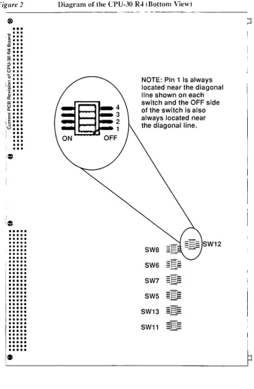
Diagram of the CPU-30 R4 (Top View) . . . \0 Fig.
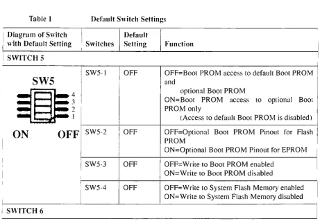
Diagram of the CPU-30 R4 (8o[[om View) . . . 11 Fig.
-
.,
Default Switch Settings . . . 12 Tab.
Front Panel Layout . . . 16 Tab. 2
Front Panel . . . 17 Fig. 3
9-pin D-Sub Connector Pinollt (RS-232) . . . 19 Tab. 3
I5-pin AU I-Ethernet Connector . . . 20 Tab. 4
Signal Assignment of the VME P2 Connector . . . 22 Tab. S
Rotary S\vilChes . . . 24 Tab. 6
SYS6XK/lOBP-1 Pin Assignment . . . 25 Tab. 7
History of t .. !anual . . . 28 Tab. S
Tables and Figures
Page 'J'abJFig.
Sarety i\otcs
1
Safety Notes
EMC
SYS68KfCPl'·30 R4
This section provides safery precautions to follow when in~talling.
oper-ating. and maintaining the SYS68K/CPU-30 R-l.
We intend to provide the necessary infomlation to in!-ltall and handle rhe SYS6XK/CPU-30 R-l in this Installation Guide. However. a!-l the product is complex and its usage manifold. we do not guarantee that the given
in-f0I111ation is complete. If you need additional infomlation. ask your Force
Computer!-l representative.
The SYS68K/CPU-30 R4 has been designed to meet the standard in-dustrial safety requirements. It must not be used except in its specific area of office telecommunication industry and industrial control.
Only personnel trained by Force Computers or persons qualified in electronics or electrical engineering are authorized to install. main-tain or operate the SYS68K/CPC-30 R4. The information given in this Illanual is meant to complete the knowledge of a specialist and must not be taken as replacement for qualified personnel.
The hoard has been tested in a Standard Force Computers system and found to comply with the limits for a Class A digital device in this system, pursuant to part 15 of the FCC Rules respectively E~
55022 Class A. These limits are designed to provide reasonable pro-tection against harmful interference when the system is operated in a commercial, business or industrial environment.
The board generates and uses radio frequency energy and. if not in-stalled properly and used in accordance with this Installation Guide. may cause harmful interference to radio communications. Operating the system in a residential area is likely to cause harmful interfer-ence, in which case the user will be required to correct the interfer-ence at his own expense.
If boards are integrated into open systems. always cover empt~ slots to ensure pl'oper EMC shielding.
Page 2
Installation
Switch
Settings
Operation
Replacement
/Expansion
Battery
Change
Electrostatic discharge and incorrect board installation and removal
can damage circuits or shorten their life. Therefore:
• Before installing or removing the board, read section 3
"Installa-tion" on page 9.
• Before touching boards or electronic components. make sure that
you are working in an ESD-safe environment.
• When plugging the board in or removing
it,do not press on the
front panel but use the handles.
• Before installing or removing an additional device or module. read
the respective documentation.
• Make sure that the board is connected to the VMEbus via both. PI
and P2, and that power is available on all power pins.
Before powering up the board check that the default switch settings
are correct as outlined in section 3.2 "Default Switch Settings" on
page 12.
When operating the board in areas of electromagnetic radiation
sure that the board is bolted on the VME system and shielded by
en-closure.
Make sure that contacts and cables of the board cannot be touched
while the board is operating.
Only replace or expand components or system parts with those
rec-ommended b)' Force Computers. Otherwise. you are fully
responsi-ble for the impact on EMC and the possibly changed functionality of
the product.
Check the total power consumption of all components installed (see
the technical specification of the respective components). Ensure that
any individual output current of any source stays within its
accept-able limits (see the technical specification of the respective source).
If
a Lithium battery on the board has to be exchanged, observe the
following safety notes:
• Incorrect exchange of Lithium batteries can result in a hazardous
explosion.
• Always use the same type of Lithium battery as is already
installed.
Sal'ety :\otes
Environment
SYS6RK/CPl'·30 R4
Always dispose used batteries and/or old boards according to your country's legislation. if possible in an environmentally acceptable
way.
Sicherheitshinwcise
2
Sicherheitshinweise
EI\1V
SYS68KiCPL-3U R4
Diesel" Abscllllitt enrhliit Sicherheitshinweise. die bei Einbau. Betrieb und
Warlung des SYS68K/CPU-30 R4 Zli beachten sind.
Wir sind cial"auf bedachl. aile notwendigen Informationen wm Einbau
llnd ZlIIll LJlllgang mil dem SYS68K/CPU-30 R4 in diesem Handbllch
be-reit Zli slellcn. Da es sich jedoch bei dem SYS68K/CPU-30 R4 llm ein
komplexes Produkt mit vieWiltigcn Einsatzmoglichkeiten handelt. kon-nen wir die VolIsl:indigkeit der im Handbllch enthaltekon-nen Informaliokon-nen nichl garanliercn. Falls Ihnen Infomlationen fehlen sollten. wenden Sic sich hiuc an Ihrcn Vertreter von Force Computers.
Das SYS6SK/CPU-30 R4 erfUllt die fUr die Industrie geforderten Sicherheitsvorschriften und darf allsschliesslich fUr Anwendungen in der Telekommunikationsindustrie und im Zusammenhang mit lndustriesteuerungen verwendet werden.
Einbau. Wartung und Betrieb durfen nur von durch Force Computers ausgebildetem oder im Bereich Elektronik oder
Elektrotechnik qualitiziertem Personal durchgefiihrt werden. Die in diescm Handhuch enthaitenen lnformationen dienen ausschliesslich dazu. das Wissen von Fachpersonal ZlI erganzen. konnen dieses
jedoch nicllt ersetzen.
Das Board wurde in einem Force Computers Standardsystem getestet. Es erfiillt die fUr digitale Geriite der Klasse A gultigen Grenzwel'te in einem solchen System gemaB den FCC-Richtlinien Abschnitt 15 bz\\,. EN 55022 Klasse A. Diese Grenzewerte sollen einen angemessenen Schutz vor SWrstrahlung beim Betrieb des Boards in Geschafts-, Gewerbe- sowie Industriebereichen gewahl'leisten.
Das Board arbeitet im Hochfrequenzbereich und erzeugt Storstrahlung. Bei unsachgema13em Einbau und anderem als in diesem Handbuch beschriebenen Betrieb konnen Storungen im Hochfrequenzhereich auftreten. Wird das Board in Wohngegenden hetl'ieben, ist del' Benutzer verpnichtet. entstehende Storungen auf seine Kosten beheben 1lI lassen.
Wenn Sic das Board ohne ein PMC Modul verwenden. schirmen Sie freie SteckpHitze mit einer Blende abo um einen ausreichenden El\IV Schutz ZlJ gewiihrleisten. Wenn Sie Boards in Systeme einhauen.
schirmen Sic t'reic Steckplatze mit einer lllende abo
Installation
Schaltereinstellungen
Betrieb
Page 6
Elektrostatisehe EntIadung und lInsaehgemiifier Ein- und Ausbau
des Boards kann Sehaltkreise besehiidigen oder ihre Lebensdaller
verkiirzen. Bcaehten Sie deshalb die folgenden Punkte:
• Lesen Sie vor Ein- oder Ausbau des Boards den Abschnitt
"Installation" auf Seite 9.
Bevor Sie Boards odeI' elektronische Komponenten
beruhren. vergewissern Sie sieh. dass Sie in einem
ESD-gesehiitzten Bereich arbeiten.
• Drucken Sie beim Ein- odeI' Ausbau des Boards nieht auf die
Frontplatte. sondern benutzen Sie die Griffe.
• Lesen Sie vor Ein- odeI' Ausbau von zllsatzlichen Geraten
oder Modulen dasjeweilige Benutzerhandbuch.
• Vergewissern Sie sich. dass das Board uber die Stecker
PIund
P2an den VME Bus angeschlossen ist und Strom an
allen Spannungskontakten anliegt.
Vcrgewissern Sic sich vor dem Hochfahren des Boards, dass die
Sehalter den in Abschnitt "Default Switch Settings" auf Seite
12beschriebenen Standardeinstellungen entsprechen.
Achten Sie darallf', dass die Umgebungs- und die
Leistungsanforderungen wahrend des Betriebs eingehaiten werden.
Wenn Sic das Board ill Gebieten mit elektromagnetischer Strahlung
bet rei ben, stellen Sie sichel', dass das Board mit dem
VMESystem
verschrauht ist und das System dureh ein Gehause abgesehirmt
wird.
Stellen Sic sieher. <lass Anschliisse und Kabel des Boards wahrend
des Betriehs nieht beriihrt werden konnen.
Sichcrhcitshinwcisc
Austallsch/Erweiterllng
Batteriewechsel
Umweltschlltz
SYS68K/CPll-30 R4
Verwenden Sie bei Austausch oder Erweiterung nur \,on Force Computers empfohlene Komponenten und Systemteile. Andernfalls sind Sie fiir mogliche Auswirkungen auf E\lV und geanderte Funktionalitiit des Produktes \'011 \'erantwortlich.
Cberpriifen Sie die gesamte aufgenornrnc Leistung aller eingebauten Komponenten (siehe die technischen Daten der entsprechenden Komponente). Stellen Sie sicher. dass die Ausgangsstrome jedes Verbrauchers innerhalb der zuliissigen Grenzwerte liegen (siehe die technischen Daten des entsprechenden Verbrauchers).
\luss eine Lithium-Batterie auf dem Board ausgewechseIt werden. beach ten Sie die folgenden Sicherheitshinweise:
• Ein unsachgemafier Wechsel yon Lithium-Batterien kann zu gefiihrlichen Explosionen fiihren.
• Verwcndcn Sie beim llatteriewechsel denselben Batterietyp. der bereits cingcsctzt wurde.
Entsorgcn Sie alte Boards gemall der in Ihrem Land giiltigen Gesetzgebung. wenn moglich umweltfreundlich.
Installation
3
Installation
Caution
Lh
Location Diagrams of the SYS6RKiCPli-30 H4
The installat ion
or
the board is easy. requiring only a power ~upply and 3VMEbus backplane. The power supply must meet the specifications
de-scribed in Table 1. "Specification~ for the CPU-30 R4 Board:' on page 7.
The processor board requires +S V supply voltage:
±
I::! V arc needed forthe RS-232 serial interface and the Ethernet Interface.
For the initial power up. a terminal can be connected to the 9-pin D-Sub
microconnector of serial port 1. which is located on the front panel. The
serial port provides RS-232 interface signal level.
Before powering up check that the default switch settings are correct as outlined in Section 3,2 'Default Switch Settings',
3.1
Location Diagrams of the SYS68K/CPU -30 R4
SYS68K/CPli·30 H4
The following two location diagrams show the important components on the top side and the bottom side of the CPU-30 R4. Both of these dia-grams only show the components on the board which are of interest to the L1ser.
Location Diagrams of the SYS6SK/CPll-3() R4 Installation Reset Switch Abort Switch AUI-Serial Port #3
Serial Port #2
[image:16.613.74.514.81.647.2]Page 10
Figure 1
Diagram of the CPlJ-30 R.J crop Viewl, - - - -
- - - ,Pmttt:
~7992 :: ~~
J 23
i
I
ITJ
Ul
I I
FORCE Gate Array
FGA-002B
IIUJIIIIIlllllUUIIIIIU1111111
r--i MC68030
i- Processor IUI;IUUI.IUIUUIUlIIIIUIlI
•
•••
•••
•••
•••
•
•
c
•
•
•
•
•
•
•
•
•
•
•
(;• •
u• •
Q•
•
II
c:c
•
c:• •
II 0• •
II
(J•
c•
0:•
ce. il w :: ;~.
I >
cce
-=~=
;. I: =
s e :
II
:e~ .~c :tc.c eco ~cc 0···
..
~'! gmltll tllIlIttt§:: MC68882 :;
¥coprocessor:'~
I~
.stitt
II Itt;,.=
411 IIUIUIIUH}!:;
I
:: J28 3: Optional
=
~ Boot PROM t:WIII 1J.1:t~
1I1111111111111111111H=
J36 - Default:: :: Boot PROM SCSI
87034 • • • • !
4HHHII'1
~--~--- \
~' .~
~",
.•
):~.
\\~
Battery
.::tlllt111tt1tiJ.
=
~:_DUS2
=
-~mnmnuJ
<'::~:"III-II-III-II-III-II-III-II~II
-£tltllt~
-
.
=
FOC-:0
:t
=
37C65C=
~numl:r
.:tlllll '" II
'r:
=
PT1EO
-~1I11111 IIltIor
• • • -II
• • • • 1
· CUI
ee ••
••••
••••
••••
a • • _: c e _ =1C C
c;1
.C%~ ,
:. :11
C 8:·
"'
·
•
",'
:•
0,...
:• •
•
0•
0•
"
•
•
• "
fit
tltlllt'1
£fttl
II I II II I ~ • • I~c,
DUS1 PT2 : : =.1'- . . : - ~ C . 8 ,
~1111I11IUu:r ~"""IHIII~
•~
,0
g
c: c: 0 (J N 11. w :: >L -_ _ _ _ _ _ _ _ _ _ _ _ _ _ _
---~
Illstallatioll
Figure 2
••
I"E : :
, mo.
~
..
~
..
a: ••
o • M •
~ :0
0.. •
U :0
'0 ::
c . 0
1.*
:0.";
..
<I> :0.
-a: :0.
co :0.
U • •
0.. • • •
. ~::: I ~:::
:u •••
I • • • I • • •
•••
•••
I • • •
1=
•••
•••
•••
•••
....
•••
•
••
• •
•
&• •
•
•
•
•
••
•
•
•
•
•
•
•
•
•
••••
•••
•••
••••
••••
••••
••••
••••
••••
••••
•
SYS68KJCPU-30 R4Location Diagrams of the SYS68KICPl"-30 R~
Diagram of the CPU-30 R~ (Bottom View)
NOTE: Pin 1 is always located near the diagonal line shown on each switch and the OFF side of the switch is also always located near the diagonal line.
SW8
SW6
= ;:
-~SW7
=E'E
-.Q>-SWS
-"E\-=EF
SW13
~
SW11
~
3 :::Del'ault Switch Settings Installation
[image:18.610.67.529.214.533.2]3.2
Default Switch Settings
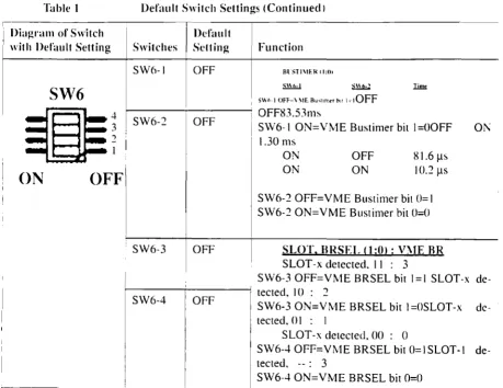
Table 1
The following table shows the defaulr settings for all the switches on rhe ~ ~
board.For the posirion of the switches on your CPU-30 R4 bmud see
Figure 2, '"Diagram of the CPU-30 R4 (Bottom Vie"v)," on page 11.
Note:
The battery backup for SRAM and RTC is disabled with thedefault switch setting. Stored data will be lost.
Default Switch Settings
Diagram of Switch I Default
with Default Setting Switches Setting Function
SWITCH
5
SW5-1
SW5
ON
OFF
SW5-2SW5-3
SW5-4
S\VITCH 6
Page 12
OFF
OFF
OFF
OFF
OFF=Boot PROM access to default Boot PROM and
optional Boor PROM
ON=Boot PROM access to optional Boot PROM only
(Access to default Boot PROM is disabled)
OFF=Optional Boot PROM Pinout for Flash PROM
ON=Oprional Boot PROM Pin alit for EPROM
OFF=Wrire to Boot PROM enabled ON=Write to Boot PROM disabled
OFF=Write to Sysrem Flash Memory enabled ON=Write to System Flash Memory disabled
SYS68K/CPU-30 R4
I
Installation Default Switch Settin~'
Table 1 Default Switch Settings (Continued 1
Diagram of Switch
I
Default
wit h Default Setting Switches Sl'tt ing Function SW6-1 OFF Bl ST/\IEIl' 1:01
~\\t.·1 , \ \ b." Iim£
SW6
S\\I·"IOFF~\\IEB",:ur.<fh" ;dOFF~
-
~
I
SW6-2 I OFFI OFF83.53ms
i SW6-1 ON= VME Bustimer bit 1 =GOFF
1.30 ms
01\
~
ON
OFF
SYS6HK}CPU-30 R~
I SW6-3 OFF
ON ON
OFF ON
81.6 1ls 1O.21ls
SW6-2 OFF=VME Bllstimer bit 0= 1 SW6-2 ON=VME Bllstimer bit O=CI
SLOT. BRSEL 0:01: V'IE BR
SLOT -x detected. I I : 3
SW6-3 OFF=V~IE BRSEL bit 1=1 SLOT-x
de-I - - - + - - - j recred. 10 : 2
SW6-4 OFF SW6-3 ON=VME BRSEL bit I=OSLOT-x de-tected. 0 I : I
SLOT-x detected. 00 : 0
SW6-4 OFF=VME BRSEL bit O=ISLOT-I de-tected. --: 3
SW6-4 ON=VME BRSEL bit 0=0
[image:19.612.71.531.82.436.2]Default Switch Settings Installation
Table I Default Switch Settings (Continued)
,
Diagram of Switch
I
SwitchesDefault
with Default Setting Setting Function
SWITCH 7
I SW7-1
I
OFFI
OFF=RESET Switch enahledSW7
I
ON=RESET SwilCh disabled4 I SW7-2 OFF OFF=ABORT SwilCh enabled
;I
ON=ABORT Switch disahled
2 !
I I SW7-3 I OFF
I
OFF=SCSI active lennination enabledI
O~
OFF
I I ON=SCSI active lemlination disabledi SW7-4 i OFF I OFF=additional VME Buslimer enabled if VME
! SIOI-1
I funclion detected (otherwise disabled)
ON=VME Buslimer disabled
SWITCH 8
SW8-1 OFF OFF=VME SIOI-1 auto-delection enabled
SW8
ON=VME slot-I function disabled4 SW8-2 OFF OFF=VME_SYSFAIL output enabled
3 ON=VME_SYSFAIL output disabled
2
SW8-3 OFF OFF=VME_SYSRESET outpUI enabled
ON
OFF
ON=VME_SYSRESET output disabledSW8-4 OFF OFF=VME_SYSRESET input enabled
ON=VrvlE_SYSRESET input disabled
SWITCH II
SWII-I ! OFF OFF=Power backup from battery disabled
SWll
ON=Power backup from battery enabled4 • SWII-2
I
OFF OFF=Power Backup from VME STBY disabled3 ON=Power Backup from VME STBY enabled
2
SWII-3 i OFF OFF=NVRAM supplied by Power Backup
dis-OFF
abledON
ON=NVRAM supplied by Power Backupen-abled
SWII-4 OFF OFF=Default NVRAM access only
ON=Optional and default NVRAM access
[image:20.610.68.530.79.651.2]Installation
Table 1
Diagram of Switch with Default Setting
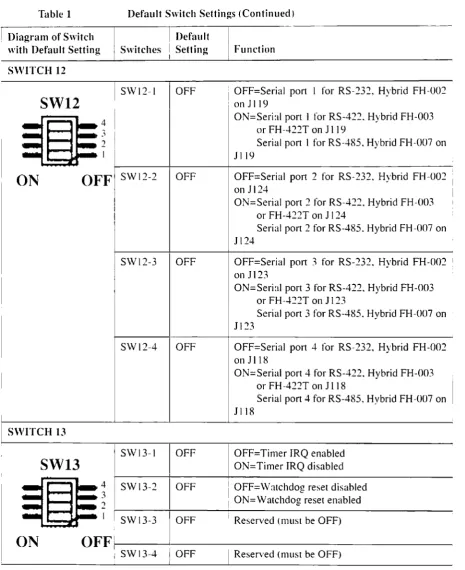
SWITCH 12
SW12
4
..,
2ON
OFF
SYS68K/CPlJ-30 R4
Default Switch Settings
Default Switch Settings (Continued)
I Default I
Switches
i
Setting I FunctionSWI2-1 OFF
SW12-2 OFF
SW12-3 OFF
SWI2-4 OFF
i OFF=Serial port I for RS-232. Hybrid FH-002
, on 11 19
ON=Serial port 1 for RS-422. Hybrid FH-003
or FH-..J.22T on 11 19
Serial port 1 for RS-485. Hybrid FH-007 on
JII9
OFF=Serial port 2 for RS-232. Hybrid FH-002 on 1124
ON=Serial port 2 for RS-422. Hybrid FH-003
or FH-422T on J 124
Serial port 2 for RS-485. Hybrid FH-007 on 1124
OFF=Serial port 3 for RS-232. Hybrid FH-002 I
on 1123
ON=Serial port 3 for RS-422. Hybrid FH-003 or FH-..J.22T on 1123
Serial port 3 for RS-485. Hybrid FH-007 on
J] 23
OFF=Serial port
-+
for RS-232. Hybrid FH-002on 1118
ON=Serial port 4 for RS-422. Hybrid FH-003
or FH -422T on 1118
Serial port 4 for RS-485. Hybrid FH-007 on JI18
OFF=Timer IRQ enabled ON=Timer IRQ disabled
I OFF=Watchdog reset disabled
I ON=Watchdog reset enabled
i Reserved (mllst be OFF)
I Reserved (must be OFF)
Front Panel
[image:22.613.200.453.195.481.2]3.3 Front Panel
Table 2
Page 16
Installation
The table below outlines the layout on the front pancl. Additionally. there
is a drawing 01" thc front panel on page 17. The front panel devices are
briefly described on the pages following the drawing.
Front Panel Layout
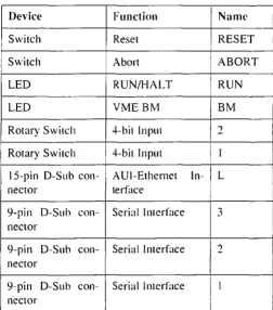
,
Device Function Name
Switch Reset RESET
Switch Abort
I
ABORTLED RUN/HALT RUN I
I
LED VMEBM BM
I
Rotary Switch 4-bit Input ')
Rotary Switch 4-bit Input 1
IS-pin O-Sub con- AUI-Ethemet In- L
I
nector terface
9-pin D-Suh con- Serial Interface 3
nector
9-pin O-Sub COll- Serial Interface 2
nector
9-pin O-Sub con- Serial Interface I
nector
Installation Front Panel
Figure 3 Front Panel
•
SYSbSKi
CPl"",1I R ..
@
RESt:t@ ABORT RESET and ABORT K~ys
0 Rll:-;
0 B~I Status LEDs
~ ~
- Rotary Swit.:hes
~ I
~
~
I I
I I
I I
L
I I
I I
I I
~
GIIS-pin D-Sub Connector
0
~
•
•
3•
•
•
9-pin D-Sub Connector0
~
•
•
2•
•
•
9-pin D-Sub Connector0
~
• •• •
1•
9-pin D-Sub Connector
I~[FI
Front Panel Installation
3.3.1 RESET and ABORT Keys
3.3.2 Status LEDs
3.3.3 \' oltage Sensor
3.3.4 Watchdog Timer
Page 18
The RESET key generales an on-board reset. The ABORT key generates all IRQ all a programmable level. Both keys call he disabled via the switches described below:
SW7-1 Description
OFF (c1e- RESET key
en-faull ) abled
I
ON RESET key
dis-I abled
I
SW7-2
I Description
I
I
OFF (clc- ABORT key en- I
fault) abled
ON ABORT key
dis-abled
The CPU-30 R4 includes two front panel LEOs: RUN/HALT LED and BM LED.
The RUN/HAL T LED displays the condition that the processor is halted or reset is active and, in this case, the LED turns red. The RUN/HALT LED turns green on nom1al operation.
The bus master BM LED is used to indicate VMEbus mastership of rhe
CPU-30 R4 and, in this case. rhe LED rurns green.
The voltage sensor generates a power-up reset if rhe vollage level is be-low 4.75 V.
This timer can be enabled by software and will generate an Nivll followed by a power-lip reset. when it is not retriggerecl
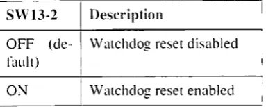
Installation Serial I/O Channels
SW 13-2 Description
OFF (de- Watchdog reset disabled
raul!)
ON I Watchdog reset enabled
3.3.5 Two Rotary Switches
Two software readable four-bit rotary switches are installed on the board and are accessible via the front panel.
[image:25.610.201.393.107.184.2]3.4 Serial
1/0
Channels
Table 3
SYS68K/CPU·30 R4
The CPU-30 R4 has three serial I/O channels available via 9-pin D-Sub connectors on the front panel. All channels will support RS-232. RS-422
and RS-4H5 interfaces via the FORCE hybrids
FH-xxx.
The defaultcon-figuration is RS-232.
The following table shows the pinout of the serial
I/O
channels forRS-232.
9-pin D-Sub Connector Pinout]) (RS-232)
Signa Directi
Pin I on Description
1 DCD in Data Channel
De-I
tector2
I
RxD in Receive Data3
I
TxD out I Transmit Data4
I
DTR out Data Tem1inalI
I
Ready5
GND-
Signal Ground6 DSR in
I
Data Set Ready7
RTS out!
Request to Send I8 CTS
I
In I Clear to Send9 GND
-
I
Signal Ground*
1. Default terminal port setup: 9600 Baud, 8 data bits, 1 stop bit, no parity.
AliI-Ethernet Installation
Note:
"'With FH-002, this signal is provided bythe
hybrid beingused. The signal DTR is always driven active and the signal DSR is always read active by software. The RS-232 interface on your current CPU-30 revision 4.x board is fully compatible to the RS-232 interface on the earlier CPU-30 revision 3.2 board. However, the default jumper settings prescribed for the earlier board mllst be used to obtain this functionality.
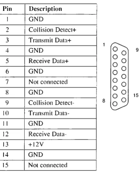
[image:26.610.188.414.376.656.2]3.5 AUI-Ethernet
Table 4
I
I
I
I
Page 20
The AUI-Ethernel Illlerface is available on the front panel via a IS-pin D-Sub connector.
The unique Ethernet address is displayed by the banner when entering the FGA Boot debugger. FGA Boot also provides a utility function (0 get the
CPU board's Ethernet address: "#40 (Ox28) Get Ethernet Number". The following table shows the pinout of the AUI-Ethernet connector
IS-pin A UI-Ethemet Connector
Pin Description I I
I GND
2
I
Collision Detect+ 3 Transmit Data+4 GND
5
Receive Data+6 GND
7 Not connected
8 GND
9 Collision
Detect-0
0
90 0
0
0
0 0
0
0
0 0
15 8
0 0
0
10I
TransmitDala-II GND
12 Receive
Data-13 +12V
14 GND
15 Not connected
Installatioll
3.6 SCSI
SCSI
The MB87033/34 provides an R-bit single-ended SCSI interface. It is routed to the V~vlEbus p~ connector.
The telmination i~ switch selectable and 'TERMPWR" i~ supported. The following switches control the SCSI termination.
S\V7-3 Description
OFF (de- SCSI active termination enabled fault)
ON SCSI active termination disabled
Note: TERMPWR is always supplied; if termination power is
supplied externally b~' a source other than the V'IE connector. the active termination is still maintained. although the VME may not be powered.
3.7 Parallel I/O (Option)
SYS68KJCPU-30 R4
The parallel I/O signals are only available with the optional 5-raw VME-bus P2 connector.
Connector Pinout for VMEhus P2 Installation
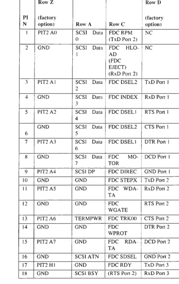
[image:28.610.163.521.145.712.2]3.8 Connector Pinout for VMEbus P2
Table 5 Signal Assignment of the VME P2 Connector
Row Z RowD
I
PI
(factory (factoryI
N option) Row A RowC i option)
I
J PIT2 AO SCSI Data FDCRPM
INC
0 (TxD Pon 2)
2 GND SCSI Data FDC HLO- NC
I AD
(FDC
I
EJECT)
I
(RxD Port 2)
3 PIT2 AI SCSI Data I FDC DSEL2 TxD Pon 1
2
4 GND SCSI Data
I
FDC INDEX RxD Pon 13
I
5 PIT2 A2 SCSI Data
I
FDC DSEL II
RTS Port I4
I
GND SCSI Data FDC DSEL2 CTS Port I
I
6 5
7 PTT2 A3 SCSI Data FDC DSELI DTR Port I
I 6
I
8
j
GND SCSI Data FDC MO- DCD Port I7 TOR
9 PIT2 A4 SCSIDP
I
FDC DlREC I GND Port I10 GND GND FDC STEPX I TxD Pon 2
II PIT2 A5 GND
I
FDC WDA-I RxD Port 2I
TA
12 GND GND
I
FDC RTS Port 2 IWGATE I
I
13 PlT2 A6 TERMPWR I FDC TRKOO CTS Porl2
I
14 GND GND
I
FDC DTR Port 2 I
WPROT
15 PIT2 A7 GND FDC RDA- DCD Port 2
TA
16 GND SCSI ATN I FDC SDSEL
I
GND Port 217 PIT2 HI GND I FDCRDY TxD Port 3 I
18 GND SCSIBSY
I
(RTS Port 2) I RxD Port 3 IInstallation
Table 5
Introduction to V\IEPRO\1 Firmware
Signal Assignment of the VME P2 Connector (Continued)
RowZ I i Row D
PI
(factory (factory1\ option) Row A RowC option)
19 PIT2 H2 SCSI ACK I GND RTS Port 3
20 GND SCSIRST
I GND CTS Port 3
21 PIT21-13 SCSI i\1SG
I (CTS Port 2)
I
DTR Port 322 GND SCSISEL I GND . DCD Port 3
23 PIT21-14 SCSI CD
I
GNDI
Gl\TI Port 324
I
GNDI
SCSI REQ I (TxD Port 3) DSR Port 1..,~
-~ PITI HI SCSI 10 I (RxD Port 3) DSR Port 2
26 GND (RTS Port I (R TS Port 3) DSR Port 3
1 )
I
27 PITI H2 GND I (CTS Port 3) PIT 1 CO
2~ GND (CTS Port
I
(TxD Port 1) PIT I CI
1 )
29 PIT] H3 DSR Port 4 lOCO Port 4 I PITI C4
(RxD POrt 1)
30 GND RTS Port 4 RxD Port 4 PIT 1 C7
31 PITI H4 I CTS Port 4 I TxD Port 4 NC
32 GND GND Port 4 I DTR Port 4 NC
Note:
The signals marked in parenthesis are only available with theuse of FH-()02 hybrids, which are available at Force Computers.
3.9 Introduction to VMEPROM Firm"rare
SYS68K/CPll-30 R4
The VMEPROM fiIll1\vare is a full multitasking multiuser real-time sys-tem. It is stored in the on-board System Flash Memory and provides the following functionality:
Configuration of the board
Starting an application
Application hooks
Shell with over 80 commands
Programming of Boot Flash devices
The SYSfJ8K/IOIW-1 Installation
[image:30.610.201.349.173.218.2]3.9.1 Booting up VMEPROM
Table 6
To start YMEPROM, the rotary switches must both be set [0
-F.
Rotary Switches
I
MODE II:
I
MODE 2The different functions of the rotary switches are described in detail in
the YMEPROM section of the SYS68KICPU-30 R4 Technical Reference
Mali/wi.
Con-ect Operation
To test the con-eel operation of the CPU board, the following command must be typed ill:
I
~
SELFTEST <CR>The selftest command tests some I/O devices. the main memory and the system timer tick inten-upt. Depending on the size of the main memory_ it may last a different amount of time (coum about one minute per mega-byte).
After all tests are done. the following message will appear on the terminal screen:
I1HEPRON Hardware Self test
I/O Lest . . . passed Hemo!"y test . . . passed Clock test . . . passed
3.10 The
SYS68K/IOBP-l
Page 24
Force Computers offers an IOBP-! back panel for easy connection of I/O signals through the YMEbus P2 connector. This board can be plugged into the YMEbus P2 connector of a YMEbus board which carries the SC-SI. FDC, and serial I/O signals on the YMEbus P2. It contains a SCSlbus connector (P2), a floppy disk imerface connector (P3), and a serial I/O connector (P5). All YMEbus P2 connector row A and C pins are routed to
Installation
Table 7
SYS6SK!CPU-30 R~
The SYS6SKiIOBP-I
the 64-pin male connector (P4). The pinollt of these connectors is ~hown
in the following table.
SYS6~K/IOBP-I Pin Assignment
PIN PIN
I
I
No. No. I I
i
IOBP Vi\IE RowA I Row B
-I bus I RowC
Signal Signal
PI (>2 J'lnemonic 1'1 nemonic Signal1'lnemonic
3~ I DB 0 SC
-SI
31 ~ DB I I SC
I
GND
I I SI
<
I
, I
30 3 DB 2 SC I Drive Select
I
~D
-14
(2)SI
29 4 DB 3
se
I - I Index FDSI
I
e
2X 5 DB4
se
-I
~rive
Select FDSI
e
27 0 DB 5
I
se
- Drive Select FDSI 2
e
26 7 DB6
!
se
-
~ Drive Select I FD, I
SI
I
3 (1)e
I
25 X DB7 SC
I - I Motor On I FD
SI
Ie
24 l) DB P
se
I -
Direction In FDSI
e
23 10 GND
-
Step FDe
""
II GNDI
-
Write Data FD--I
e
21 12 GND
I
I
GND
I
Write Gate I FD,
I I
e
20 13 TERMP-
. se
- I Track 000 , FDWR
I
SII
C19 14 GND
I
I-I
Write Protect FDC
18 15 GND
I
-
I Read DataI
~D
The SYS6SKfIOBP-l Installation
Table 7 SYS68K!IOBP-l Pin Assignment (Continued)
PIN
PIN
No. No.
10BP VIVIE RowA RowB
-1 bus Row C
Signal Signal
PI P2 I\lnernonic Mnemonic Signal \lnemonic
17
16 ATN SC-
Side Select FDI
SI C
16
17
GND-
FDC READY,
FD C
I
15
IH
BSY SC-I SJ
14 19 ACK SC
-
GNDSI
13
20
RST SC - GND I ,SI I
I
12
21
MSG SC-SI
II
22
SEL SC GND GNDSI
10 23
C(D
SC-
GNDSI
9
24
REQ SC-SI
8
25
1/0 SC-SI
7
26
-6
27
GND - Reserved II
~
28
-
Reserved29
DSR SE-
DCD SEI R R I
3 30 RTS SE - RXD SE
R R
2
31
CTS SE GND TXD SEI
R R
1
32
GND SE-
DTR SER , R
Installation The SYS68K/IOBP·]
History of Manual Publication
4
Historv of Manual Publication
.., [image:34.610.199.527.179.654.2]Below is a description of the publication history of this srS68KICPU-3U R4
installation Guide.
Table 8 History of Manual
Edition No. Description
I
Date
II First Print February 1996
I
2
Descliprion of switch May 1996 SWII-3 in table 1has been corrected
3 Revised safety note October 1996 I
I
4 '"AUI-Ethernet" has January 1997
I
been changed.
5
Configuration of seri- January 199R Ial ports 1-4 for
RS-232. 422
and485
completed, location diagram and switchI
settings of SW12 in :
table I updated
6.0 Section "Safety September 1999 I
Notes" included i
7.0 Editorial changes November 1999 I
R.O/AA Editorial changes, September 2001 I
added section !
"Sicherheitshin-weise"
9.0/AB Corrected section September 2001
'"Sicherheitshin-weise" I
January 2002 !
AC Editorial changes: I
updated title page I
and address page. added copyright page
I
Product Error Report
Product:
Serial No.:
Date Of Purchase:
Originator:
Company:
Point Of Contact:
Tel.:
Ext.:
Address:
Present Date:
Affected Product:
Affected Documentation:
:l Hardware :l Software :l Systems :. Hardware :l Software :l Systems
Error Description:
This Area to Be Completed by Force Computers:
Date:
PR#:
Responsible Dept.:
u
Marketing
:JProduction
Engineering ....
0
Board 0 Systems
A SOLECTRON COMPANY
World Wide Web: www.forcecomputers.com
24-hour access to oil-line manuals. driver updates. and application notes is provided via SMART. our SolutionsPLUS customer support program that provides current technical and services information.
The Americas
Force Computers Inc.
4305 Cushing Parkway Fremont. CA 94538 U.S.A.
Tel.: +1 (510) 445-6000 Fax: +1 (510) 4'15-6001 Email: [email protected]
2(~)29 420 (kKI AC
Headquarters
Europe
Force Computers GmbH
Prof.-Messerschrnitt-Str. ( D-85579 Neubiberg/Munchen Germany
T(>I.: +49 (89) 60814-0 Fax: +'19 (89) 609 77 93 Email: [email protected]
Asia
Force Computers Japan KK
Shibadairnon tvlF Building 4F 2-(-(6 Shiba Daimon
Minato-ku. Tokyo 105-0012 Japan