2016 International Conference on Electronic Information Technology and Intellectualization (ICEITI 2016) ISBN: 978-1-60595-364-9
Designing and Application of
∏
-
type
Miniaturized Lumped Equalizer
Yi Wang, Yuntao Chen, Yongliang Zhou and Han Fu
ABSTRACT
A novel lumped equalizer is presented in this paper. The equalizer is constructed with ∏-type lumped network. The theory of the structure is analyzed and the derivation of element values is discussed with application. The simulation results are in agreement with theoretical deduction. The test results in transmitter application show that the gain fluctuation of ±2dB can be reduced to ±0.3dB in the working frequency 0.2-1GHz. The test results are in good agreement with the design values.
INTRODUCTION
The connecting cable coupled with external elec Broadband RF system is an integral part of broadband communication networks, electronic warfare, radar and other equipment broadband indispensable.
In order to ensure the performance of the whole system requires a broadband RF systems more instantaneous bandwidth wide enough, the broadband RF transmitter system must have a good amplitude-frequency characteristics.
Broadband RF transmitter system performance according to different needs, in addition to a multi-stage amplifier, it will also cascaded switches, attenuators, splitters and other devices, at all levels of the circuit gain (or loss) unevenness superposed on each other and influence, seriously the deterioration of the transmitter band unevenness, leading to deterioration of the output waveform.
________________________
Digitally controlled attenuator ways to improve gain flatness [1], but cannot gain flatness instantaneous bandwidth can be adjusted. In the transmitter inserted into the appropriate location equalizer, using the equalizer positive slope (negative slope, or parabolic) amplitude-frequency characteristics to compensate for unevenness in-band transmitters to improve the transmitter in-band amplitude-frequency characteristics.
Traditionally, the use of a waveguide or coaxial equalizer to construct [2,3], often larger, the weight is too heavy, not easy to integrate, not suitable for small broadband RF devices.
Micro strip circuit has a low profile, easy processing, light weight, etc., micro strip equalizer plane has been widely studied and applied [4-6].
In order to achieve a better SWR in a wide band, micro strip equalizer usually more minor structure. Different sizes of micro strip circuit will make minor structural complexity, larger size, and most of its design relies on tuning and optimization of simulation software, lack of theoretical basis, design difficulties.
Especially at low frequencies, larger micro strip structure is not conducive to miniaturization of systems. Lumped capacitors, inductors, to achieve load resistor set by way of its total balance at frequencies below 3GHz can effectively reduce the circuit size, but single-stage aggregate equalizer standing poor[7]. Equalizer Π-type structure [8] can be optimized to achieve a better balance of properties in six octave.
Aiming lumped equalizer Π structure of theoretical analysis, the use of odd - even mode analysis method to derive equalizer scattering parameters are a measure to a comprehensive component values based on the target, some effective methods of total equalizer design Π-type collector. Finally, the validity of the total combined application equalizer sets.
THEORETICAL ANALYSIS AND DESIGN
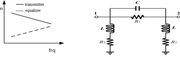
Figure 1. amplitude-frequency characteristics. Figure 2. Π type lumped equalizer Schematic.
Amplitude-frequency characteristics of Series capacitance and inductance ground is expressively rising curve, equalizer structure shown in Figure 2. It can be known that series capacitance and inductance ground combined are combined to achieve broadband impedance matching, load resistance combined to regulate amplitude-frequency curve slope. Using the odd - even mode method, scattering parameters can be drawn as follows:
) )( ( ) -( 21 S O S e S e O Y Y Y Y Y Y Y S
(1)
) )( ( -2 11 S O S e e O S Y Y Y Y Y Y Y S
(2)
Where in, YO, Ye are even and odd mode input admittance, YS source admittance. YO, Ye can be gotten in the follow:
1 2 2 2 1 2 1 ) ( 2 -2 2 2 R R L j LC C R R j L j R R YO
(3)
2 1 R L j Ye
(4)
2 1
-21
11
S e
e S
Y Y
Y Y S
S (5)
The ω= 6.28G rad / s and R2 = 68.9 Ohm into the formula (5), can be obtained by L = 18.5nH. In at 1GHz, the following relationship:
2 1 =
21
S (6)
The ω = 6.28 Rad / s, R1 = 153.8 Ohm, R2 = 68.9 Ohm and L = 18.5nH into the formula (1) and (6), can be obtained C = 4.9pF.
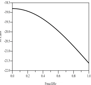
[image:4.612.331.481.277.416.2]
(a)Simulation resultsof S21. (b) Simulation results of S11. Figure 3. S-parameter simulation.
Schematic simulation based on component values were calculated in software, the simulation results shown in Figure 3. FIG. 3 (a), the DC loss 8dB, loss of 7.5dB 200MHz at a loss at 1GHz is 3dB, 0.2-1GHz are measured as 4.5dB. FIG. 3 (b), the in-band return loss is less than -18.5dB, equalizer having good matching characteristics.
TEST RESULT
equipment 9 m long RF cable, etc. the overall gain flatness of the transmitter was deteriorated for each device cascading , and the fluctuation range was up to 4dB. To improve gain flatness, lumped equalizer was cascaded before the second stage amplifier. It can be made surface-mount configuration, as shown in the fig 4. The size is 9.9 * 9.5mm2, cascaded in the transmitter, it does not substantially affect the overall size of the transmitter.
[image:5.612.183.409.343.491.2]
(a) equalizer test board (b)Surface Mount equalizer Figure 4. Equalizer physical picture.
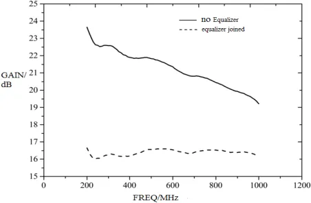
Figure 5. Amplitude-frequency curve before and after cascading equalizer.
The equalizer is cascaded to the transmitter, which greatly improved the in-band gain flatness, as shown in Figure 5. For joining the equalizer, band ± 2dB fluctuation is reduced to ± 0.3dB, to achieve the desired objectives.
CONCLUSION
transmitter indicated that the equalizer can better improve the flatness of the equalizer provides a new way to design.
REFERENCES
1. Zhikun Guo, ADS-based broadband wireless transmitter gain flatness compensation method. Information and Communication [J], 2013, 128 (6): 75-77.
2. Jihui G. and Yinxia Z. “The design of coaxial microwave amplitude equalizer.” 2008 China-Japan Joint Microwave Conference, 2008: 526-529.
3. Zhang Y. “Research on the millimeter wave power equalizer.” IEEE 2007 International symposium on Microwave, Antenna, Propagation, and EMC Technologies for Wireless Communication. Aug. 2007: 446-449.
4. Han Lei. the study of low VSWR balanced micro strip. Modern radar [J]. 2010, 32(5): 76-78. 5. Dalong Lv. Broadband amplitude equalizer design, Journal of Microwaves [J], 2012, 28 (5):
93-96.
6. Li Jian. Design and Implementation of X-band broadband low loss power equalizer. Modern radar [J], 2011, 33 (3): 67-69.
7. Fejzuli, A.R. Kaarsberg. and N. Roldan. “Broadband amplifier gain slop equalization with a single passive component.” High Frequency Electronics, June 2006