© 2017, IRJET | Impact Factor value: 5.181 | ISO 9001:2008 Certified Journal
| Page 189
Design and Implementation of Phase Frequency Detector Using Different
Logic Gates in 45nm CMOS Process Technology
Hiren B. Ravisaheb
1, Bharat H. Nagpara
21
P.G. Student, Dept. of EC, C. U. Shah College of Engineering & Technology, Wadhwancity ,Gujarat
2Asst. Prof. , Dept. of EC, C. U. Shah College of Engineering & Technology, Wadhwancity, Gujarat.
---***---Abstract -
The Phase Detectors determines the relativephase difference between the two incoming signals and outputs a signal that is proportional to this phase difference. The phase detector also detects the frequency error; they are called Phase Frequency Detectors (PFD). It is very important block for the Clock and Data Recovery circuit. This paper presents the different design schemes of the PFD and compares them with their output results. The PFD is implemented with True Single Phase Clocked logic. The circuits that have been considered are the PFD using NAND Gate, PFD using NOR Gate and PFD using AND Gate. The different PFD circuits are designed and simulated on LT Spice Tool using 45nm CMOS process technology with supply voltage 1 V.
Key Words:
Phase Frequency Detector, Phase locked loop,
True Single Phase Clocked, LT Spice Tool.
1. INTRODUCTION
The rapid growth in wireless applications in last decade has motivated to design fully integrated, low power, low cost and high performance transceivers. The Clock and Data Recovery circuit is most importance in wireless communication device which is useful to generate clock and recover the data. Clock and Data Recovery finds wide application in the area such as Serial data communication, Repeater, satellite communication, optical transceiver, chip to chip interconnects etc.
PFD in PLL is used to detect the phase as well as frequency difference between the two signals that is reference signal and the output from VCO as compare to the phase detectors which are capable of detecting the phase difference only. The characteristics of PFD have huge impact on performance of PLL. The lock time and timing jitter of a PLL are largely affected by the
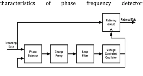
[image:1.595.310.558.223.354.2]characteristics of phase frequency detector.
Fig. 1 Clock and Data Recovery circuit
2. CIRCUITS ARCHITECTURE
2.1 NAND gate based PFD
© 2017, IRJET | Impact Factor value: 5.181 | ISO 9001:2008 Certified Journal
| Page 190
Fig.3 NAND Gate based PFThe PFD is implemented with True Single Phase Clocked logic. The design strategy is to minimize the number of transistors and the amount of power consumed. However, not all of the transistors can be implemented with minimum width such as those involved in the reset operation. The schematic of PFD using NAND Gate is shown in Fig.4.
Fig.4
Schematic of NAND Gate based PFD2.2 NOR gate based PFD
PFD using NOR gate is shown in figure.5. The circuit consists of two resettable, edge triggered D flip flopswith their D inputs tied to logic 1 and a NOR Gate in the reset path. The Ref and Div serve as clocks of the flip flops. The UPb and DNb signals are given as input to the NOR gate. Suppose the rising edge of Ref leads that of Div, then UPb goes to logic low i.e. UP keeps high until the rising edge of Div makes DNb on low level. Because UPb and DNb are NORed, so Reset goes to logic high and resets the PFD into
the initial state.
Fig.5 NOR Gate based PFD
The schematic of NOR Gate based PFD shown in Fig.6 which consisting of only 20 transistors.
Fig.6 Schematic of NOR Gate based PFD
2.3 AND gate based PFD
© 2017, IRJET | Impact Factor value: 5.181 | ISO 9001:2008 Certified Journal
| Page 191
Fig.7 AND Gate based PFDThe schematic of AND gate based PFD circuit consisting of only 22 transistors is shown in Fig.8
Fig.8 Schematic of AND Gate based PFD
3. SIMULATION RESULTS
The PFD is a state machine with three states. When Ref leads Div, the UP output is asserted on the rising edge of Ref. The UP signal remains in this state until a low to high transition occurs on Div. At that time, the DN output is asserted causing both the flip flops to reset through the asynchronous reset signal. There is a small pulse on the DN output, whose duration is equal to the delay through the logic gates and the reset delay. The pulse width of the up pulse is equal to the phase error between the two signals.Here, Ref signal is equal to the Data Signal and Div signal is equal to the Clock signal.
3.1
AND Gate PFD simulation
Fig.9 when data signal leads the clock signal
Fig10. When clock signal leads the data signal
© 2017, IRJET | Impact Factor value: 5.181 | ISO 9001:2008 Certified Journal
| Page 192
3.2 NAND gate PFD simulationFig.12 when data signal leads the clock signal
[image:4.595.31.289.108.577.2]Fig.12 When Clock signal leads data signal
Fig.13 when both clock and data signal are same
4. PERFORMANCE COMPARISON
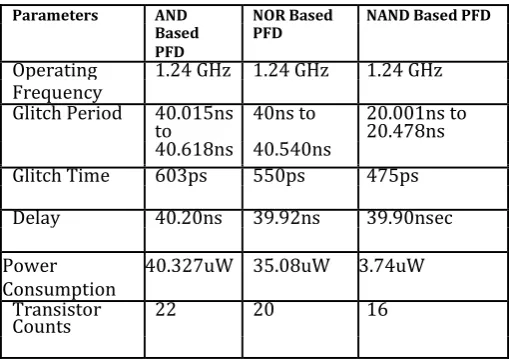
[image:4.595.37.286.118.249.2]Table I represents various parameters for the different PFDs when they are designed on LT Spice. It is seen that NAND based PFD has the minimum power consumption and occupy less area compared to the other two. They all have the same range of operating frequency. Dead Zone problem is also negligible for the NAND Based PFD.
Table I: Comparison between different PFD
Parameters AND NOR Based NAND Based PFD
Based PFD
PFD
Operating 1.24 GHz 1.24 GHz 1.24 GHz Frequency
Glitch Period 40.015ns
to 40ns to 20.001ns to 20.478ns 40.618ns 40.540ns
Glitch Time 603ps 550ps 475ps
Delay 40.20ns 39.92ns 39.90nsec
Power
Consumption 40.327uW 35.08uW 3.74uW Transistor
Counts 22 20 16
5. CONCLUSION
Minimization of power consumption is essential for high performance VLSI systems. This paper compares the performance of Phase Frequency Detectors by different Logic Gates .As can be seen from the simulation results AND based PFD consumes maximum amount of power among all the PFDs and has highest delay. NOR based PFD consumes more area and power compared to the NAND based PFD. Therefore, in order to have low power consumption and smaller area we use NAND based PFD.
ACKNOWLEDGEMENTS
I am thankful to my parents, my special friends to motivate me and to increase my confidence. I am thankful to B.H.Narpara to guide me. And finally I am thankful to hidden energy to stay always with me.
REFERENCES
[1] Ching-Che Chung and Chen-Yi Lee, “A New DLL-Based Approach for All-Digital Multiphase Clock Generation,” IEEE Journal of Solid -State Circuits, vol. 39, no 3, March 2004, pp469-475.
[2] S. B. Rashmi and Siva S. Yellampalli, “Design of Phase Frequency Detector and Charge Pump for High Frequency PLL,” International Journal of Soft Computing and Engineering, vol.2, Issue-2, May 2012, pp 88-92. [3] Evan Lee Eschenko “A low power prescaler, phase frequency detector and charge pump for a 12 GHz frequency synthesizer,” A Thesis of Master of Science, Office of Graduate Studies of Texas A&M University, Dec 2007.
[image:4.595.308.563.123.303.2]© 2017, IRJET | Impact Factor value: 5.181 | ISO 9001:2008 Certified Journal
| Page 193
[5] K.Khare, N.Khare, P. Deshpande and V. Kulhade,“Phase Frequency Detector of Delay Locked Loop at High Frequency,” lCSE Proc.2008, Johor Bahru, Malaysia,pp 113-116.
[6] V.Lule and V.Nasre, “Area efficient 0.18um CMOS phase frequency detector for high speed PLL”, International Journal of Engineering Scientific and Research Publication, vol.2, Feb.2012, pp 1-3.