N A N O E X P R E S S
Open Access
AlGaInP LED with low-speed spin-coating silver
nanowires as transparent conductive layer
Xia Guo
1*, Chun Wei Guo
1, Cheng Wang
2, Chong Li
1and Xiao Ming Sun
2Abstract
The low-speed spin-coating method was developed to prepare uniform and interconnected silver nanowires (AgNWs) film with the transmittance of 95% and sheet resistance of 20Ω/sq on glass, which was comparable to ITO. The fitting value ofσdc/σopof 299.3 was attributed to the spin-coating process. Advantages of this solution-processed AgNW film on AlGaInP light-emitting diodes (LEDs) as transparent conductive layer were explored. The optical output power enhanced 100%, and the wavelength redshift decreased from 12 to 3 nm, which indicated the AgNW films prepared by low-speed spin-coating possessed attractive features for large-scale TCL applications in optoelectronic devices.
Keywords:AlGaInP; Light-emitting diodes (LEDs); Low-speed spin-coating; Silver nanowires; Transparent conductive layer
Background
Transparent conductive layer (TCL) is crucial for light-emitting diodes (LEDs) which spread the carriers far away from the opaque electrodes to enhance the quantum ef-ficiency and improve the efef-ficiency droop effect [1-3]. Indium-doped tin oxide (ITO) material is widely used in LED field with the sheet resistance Rs of 10 to 30 Ω/sq and optical transmittanceTof 90%, which are two import-ant figures of merit (FoM) to facilitate to describe the per-formance of TCLs [4]. However, due to the scarcity of the element indium in the earth and consequently the soaring prices, recently, nanomaterials, such as carbon nanotubes (CNTs) [5], graphene [6], metal grids [7], and metallic nanowires [8], have attracted great attention as candidates of TCL due to their unique electrical properties, good transparency, and mechanical flexibility. Due to the large inter-junction resistance of CNT film caused by mixture of metallic and semiconducting properties, the sheet re-sistance of CNT film is 200 to 1,000 Ω/sq [9], which is relatively high compared with that of the ITO film. Gra-phene has high mobility as well as high transmittance [10,11]. However, large sheet resistance and obvious deg-radation of graphene layer under several milliampere current injections restricted its actual application [12].
Random and sparse silver nanowire (AgNW) film [13], which demonstrated superior FoM performances, was regarded as the most promising candidate to replace ITO, due to its low inter-wire junction resistance and low ab-sorption loss [14]. Yi’s group demonstrated solution-processed AgNW films withT550nmof 80% andRsof 20Ω/ sq [9]. J. N. Coleman’s group sprayed the AgNWs over large areas with T550nm of 90% and Rs of 50 Ω/sq [15]. Such AgNW films as TCLs applied to organic optoelectronic de-vices were reported. For example, AgNWs film as top elec-trodes of the organic solar cells or organic LEDs were recently established as a serious alternative to ITO [16-18].
One of the most significant challenges for the AgNW film was to obtain the low sheet resistance and high transmittance at the same time [19]. Besides controlling the diameter and length of the wires, uniform distribu-tion of the wires was another important factor. Conven-tional drop-coating, spray-coating, and bar-coating processes inevitably caused the solution-based AgNWs self-aggregation after solvent drying process. Poor adhe-sion to the substrate made the uniform distribution of AgNWs more difficult. Thus, new film coating method as well as substrate material to improve the uniformity of nanowire distribution was required. Filtration coating was developed for preparing AgNW films withTof 88% at 550 nm and Rs of 12 Ω/sq on cellulose nanopaper [20]. Exfoliated clays were utilized for reducing the self-aggregation of nanowires with high solution viscosity on
* Correspondence:guo@bjut.edu.cn 1
Photonic Research Lab, Beijing University of Technology, Beijing 100124, People’s Republic of China
Full list of author information is available at the end of the article
PETs by roll-to-roll coating process withT of 97.9% and
Rsof 91.3Ω/sq [16].
In this paper, a low-speed spin-coating method was developed for uniform AgNW film with the T of 94% andRsof 20Ω/sq on glass. The optical output power in-creased about 100% for AlGaInP LEDs with AgNW film as TCL, and the wavelength redshift decreased from 12 to 3 nm under the current injection of 100 mA due to the uniform carrier injection in the active region.
Methods
The Ag nanowires were prepared following the reported procedure [21]. In brief, 0.5 g of glucose and 0.1 g of polyvinyl pyrrolidone (PVP) were dissolved in 35 ml of deionized water to form a clear solution. Then, 0.5 ml of freshly prepared 0.1 M aqueous AgNO3 solution was added under vigorous stirring. The mixture was trans-ferred into a 40-ml Teflon-sealed autoclave and heated at 140°C for 10 h. After the reaction, the autoclave was allowed to cool in air and the product was purified by 3 to 5 centrifugation/rinsing/redispersion circles. Then, the AgNWs re-dispersed in isopropyl alcohol due to bet-ter dispersibility for different concentrations. The AgNW film was fabricated through spin-coating at a speed of 270 rpm, which was much lower than the spin-coating speed of photoresist which was used in the microelec-tronics field due to the poor adhesion of AgNW solu-tion. The nanowires were stuck on the substrate surface after the solution was spanned out of the substrate. After the spin-coating process, samples with AgNW film was put on the hot plate for 10 min with a temperature of 200°C in order to decrease the nanowire-nanowire con-tact resistance [22].
Results and discussion
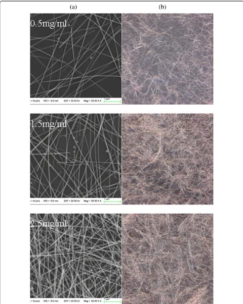
Figure 1a presented the scanning electron microscopy (SEM) images of AgNW films on glass prepared by spin-coating, which was the mostly commonly used in pre-paring photoresist with large scale in the field of inte-grated circuits. The concentrations of AgNW solution were 0.5, 1.5, and 2.5 mg/ml, respectively. The rotation speed was closely related with the FoM and was opti-mized to be 270 rpm, which was far lower than that in the photolithography process due to the poor adhesion of wires to the substrate. From the SEM images, the typ-ical diameter and length of the AgNWs can be measured about 40 nm and 30–50μm, respectively. But most im-portantly, the wires connected were with each other and uniformly distributed, which guaranteed low resistance of the AgNW film. Figure 2b showed the corresponding microscopic photographs with magnification of × 1,000, which also displayed the uniform distribution of the AgNW films. By increasing the AgNW concentrations, the AgNW area coverage increased. For the concentration
of 2.5 mg/ml, it is hard to find the bare space of substrate under the microscope, which indicated low transmittance.
Figure 2a showed the transparent conductive perfor-mances of AgNW film on glass without any pressing treat-ment after spin-coating. The transmittance was evaluated using a piece of bare glass as reference. The sheet resis-tances of AgNW film on glass prepared by spin-coating at 270 rpm showed 20Ω/sq with T550nm of about 95%. It should be noted that the value (Rs,T550nm) of (20 Ω/sq, 95%) was comparable with the performance of ITO and was much superior to that of graphene and CNT, which indicated that the AgNW film as transparent conductive layer was capable of applications in the optoelectronic de-vices, such as LEDs and solar cells, whose performance was sensitive to the power conversion efficiency. Figure 2b showed the spectral transmittance of AgNW film on glass with the AgNW concentrations from 0.25 to 3.5 mg/ml. The transmittance was kept almost flat from about 420 to 800 nm for all the curves, which indicated wide applica-tions in the visible wavelength range. The transmittance decreased with the concentration of AgNW solution due to the nanowire coverage area.
The transmittance and sheet resistance of nanowire film could be expressed as [23]
Tð Þ ¼λ 1þ Z0 2Rs
σop σdc
−2
ð1Þ
in which Z0 was the impedance of free space which was equal to 377 Ω. Rs was the sheet resistance of the nanowire film.σopandσdcwere the optical and DC con-ductivity of the film, respectively. The optical and elec-trical performance of the film could be evaluated by the ratio ofσdc/σop. High transmittance and low sheet resist-ance means the large ratio of σdc/σop. The first criterion for high-performance TCL required the ratio ofσdc/σop≥ 35 to achieve the target of T≥90% and Rs≤100 Ω/sq [14]. In our experiment, theσdc/σopof the film prepared by spin-coating was fitted to be 299.3, as shown in Figure 2a, which was close to that of ITO and much larger than that of CNT and graphene [14,24]. Also, the theoretical prediction fitted all the experimental data very well except the only data with the concentration of 0.25 mg/ml. For comparison, the sheet resistance of AgNW film prepared by conventional drop-coating on glass was 1,000 Ω/sq withT550nm of about 95%, and the fitting ratio ofσdc/σopwas only about 31, which indicated that the low-speed spin-coating could improve the FoM of the AgNW film greatly by enhancing the uniformity of nanowire distribution.
LEDs, was smaller work function difference of no more than 1.5 eV between the AgNW and GaP, which indi-cated the feasibility of ohmic contact between metal nanowire and p-doped GaP.
[image:4.595.57.290.88.433.2]The AlGaInP LEDs were grown on n-GaAs substrate by metal-organic chemical vapor deposition. The details could be found in ref. [25]. In order to study the current-spreading effect of AgNW film, only 500-nm-thick Mg-doped p-GaP window layer with the doping density of 5 × 1018 cm−3was grown on top. The 50-, 150-, or 200-nm-thick Au/BeAu/Au with 100μm diameter was first depos-ited and then patterned by wet etching as p-type electrode. The AgNW solution with the concentration of 0.5 mg/ml was applied and then stuck on the surface of the LED wafer by Vander Waals force. The chip size was 300μm × 300μm in this work.
Figure 3 showed the current–voltage (I-V) curves of AlGaInP LED with and without AgNWs as current-spreading layer with the voltage drops of 2.08 and 2.18 V at current injection of 20 mA, which indicated better current spreading. The inset showed the micro-scope photographs of LED wafers before dicing under the current injection of 5 mA under the probe station. It was obvious that the current-spreading effect was totally different, which echoed the I-V measurement results. For the devices without AgNWs, the emission was local-ized around the electrode, which indicated the carriers transport laterally with limited distance. While for the devices with AgNW film, the whole wafer was lighting up, which demonstrated the excellent capability of lat-eral carrier transport of AgNW film.
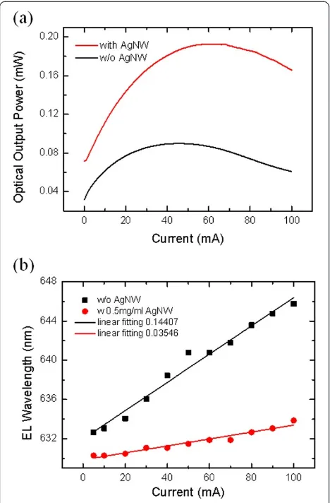
Figure 4a demonstrated the optical output power on the current injection of LED with and without AgNW film as TCL. The optical output power and the linearity of LED with AgNW film were much better than that of without AgNW film. At 20 mA, the optical output power of LED with AgNW film was two times of that of without AgNW film. As we known, the optical output power improved only 30% if ITO as TCL on LEDs [26,27]. Nano or microstructures, such as photonic crystal and surface roughness, could only improve the optical out-put power about 10% to 30% [28]. The current value corre-sponding to the maximum optical output power was 60 and 40 mA, respectively, with and without AgNW film, which indicated the better thermal performance. The peak wavelength was 630 and 635 nm, respectively, according to the electroluminescence spectra of LEDs with and without AgNW film at 20 mA. The wavelength redshift was another important criterion to characterize the current-spreading effect, and AlGaInP material was very sensitive to the temperature. Figure 4b demonstrated
[image:4.595.305.538.524.685.2]Figure 3Current-voltage (I-V) curves of AlGaInP LED with and without AgNWs as current-spreading layer.The inset showed microscope photographs of LED wafers before dicing under the current injection of 5 mA under the probe station.
the wavelength redshift measurement results, in which the dots were the measurement data and the line was the linear fitting of the data. The wavelength redshift was 3 and 12 nm for LEDs with and without AgNW film, respectively, which verified the optical output power results.
The obvious improvement of LED’s optical output power and thermal performance, we believe, not only due to the high FoM of AgNW film but also due to the current injection in different ways. The network of nanowires on the LED formed an equipotential connec-tion after biasing. All the nanowires uniformly distrib-uted on the surface of the LED injected the carriers at the same time with lowered current density, just like water from a shower head. Compared with the current injection from the ohmic contact electrode which usu-ally located at the center of the device, the current dens-ity distribution in the quantum wells from the nanowire
film will be more uniform, which decreased the current crowding and heat generation.
Conclusions
In summary, low-speed spin-coating method was dem-onstrated to prepare uniform and interconnected AgNW film with the transmittance of 95% and sheet resistance of 20Ω/sq on glass, which was comparable to ITO. The fitting value of σdc/σopof around 300 was attributed to the spin-coating process. Advantages of this solution-processed AgNW film on AlGaInP LEDs as TCL were explored. The optical output power enhanced 100% and the wavelength redshift decreased four times, which in-dicated the AgNW films prepared by low-speed spin-coating-possessed attractive features for wide TCL appli-cations in optoelectronic devices.
Competing interests
The authors declare that they have no competing interests.
Authors’contributions
GX and GCW drafted the manuscript. GX conducted the experiment design and analysis of all the experiments. GCW carried out most of the
experimental work including all the measurements. WC prepared the AgNW solution. LC and SXM participated in all the discussion on this study. All authors read and approved the final manuscript.
Acknowledgements
This work was supported by the National Natural Science Foundation of China (Grant Nos. 61222501 and 61335004) and the Specialized Research Fund for the Doctoral Program of Higher Education of China (Grant No. 20111103110019).
Author details
1Photonic Research Lab, Beijing University of Technology, Beijing 100124,
People’s Republic of China.2Beijing University of Chemical Technology,
Beijing 100029, People’s Republic of China.
Received: 23 September 2014 Accepted: 25 November 2014 Published: 11 December 2014
References
1. Kim A, Won Y, Woo K, Jeong S, Moon J:Transparent electronics: all‐solution‐ processed indium‐free transparent composite electrodes based on Ag nanowire and metal oxide for thin‐film solar cells (Adv. Funct. Mater. 17/2014).Adv Funct Mater2014,24:2414.
2. Yusoff A, Bin Mohd R, Lee SJ, Shneider FK, Da Silva WJ, Jang J: High-performance semitransparent tandem solar cell of 8.02% conversion efficiency with solution-processed graphene mesh and laminated Ag nanowire top electrodes.Adv Energy Mater2014,12:4.
3. Shim J, Han D, Kim H, Shin D, Lin G, Meyaard DS, Shan Q, Cho J, Schubert EF, Shim H:Efficiency droop in AlGaInP and GaInN light-emitting diodes.
Appl Phys Lett2012,100:111106.
4. Chae DJ, Kim DY, Kim TG, Sung YM, Kim MD:AlGaN-based ultraviolet light-emitting diodes using fluorine-doped indium tin oxide electrodes.
Appl Phys Lett2012,100:81110.
5. Feng C, Liu K, Wu JS, Liu L, Cheng JS, Zhang Y, Sun Y, Li Q, Fan S, Jiang K: Flexible, stretchable, transparent conducting films made from superaligned carbon nanotubes.Adv Funct Mater2010,20:885–891. 6. Pang S, Hernandez Y, Feng X, Müllen K:Graphene as transparent
[image:5.595.57.291.89.445.2]electrode material for organic electronics.Adv Mater2011,23:2779–2795. 7. Hsu P, Wang S, Wu H, Narasimhan VK, Kong D, Lee HR, Cui Y:Performance enhancement of metal nanowire transparent conducting electrodes by mesoscale metal wires.Nat Commun2013,4:2522.
8. Garnett EC, Cai W, Cha JJ, Mahmood F, Connor ST, Christoforo MG, Cui Y, McGehee MD, Brongersma ML:Self-limited plasmonic welding of silver nanowire junctions.Nat Mater2012,11:241–249.
9. Hu L, Kim HS, Lee J, Peumans P, Cui Y:Scalable coating and properties of transparent, flexible, silver nanowire electrodes.ACS Nano2010, 4:2955–2963.
10. Biswas C, Lee YH:Graphene versus carbon nanotubes in electronic devices.Adv Funct Mater2011,21:3806–3826.
11. Bonaccorso F, Sun Z, Hasan T, Ferrari AC:Graphene photonics and optoelectronics.Nat Photonics2010,4:611–622.
12. Youn D, Yu Y, Choi H, Kim S, Choi S, Choi C:Graphene transparent electrode for enhanced optical power and thermal stability in GaN light-emitting diodes.Nanotechnology2013,24:75202.
13. Michaelson HB:The work function of the elements and its periodicity.
J Appl Phys1977,48:4729–4733.
14. De S, Coleman JN:The effects of percolation in nanostructured transparent conductors.MRS Bull2011,36:774–781.
15. Scardaci V, Coull R, Lyons PE, Rickard D, Coleman JN:Spray deposition of highly transparent, low‐resistance networks of silver nanowires over large areas.Small2011,7:2621–2628.
16. Kim T, Kim YW, Lee HS, Kim H, Yang WS, Suh KS:Uniformly interconnected silver‐nanowire networks for transparent film heaters.Adv Funct Mater 2013,23:1250–1255.
17. Krantz J, Stubhan T, Richter M, Spallek S, Litzov I, Matt GJ, Spiecker E, Brabec CJ: Spray‐coated silver nanowires as top electrode layer in semitransparent P3HT: PCBM‐based organic solar cell devices.Adv Funct Mater2013, 23:1711–1717.
18. Krantz J, Richter M, Spallek S, Spiecker E, Brabec CJ:Solution‐processed metallic nanowire electrodes as indium tin oxide replacement for thin‐film solar cells.Adv Funct Mater2011,21:4784–4787.
19. Song M, You DS, Lim K, Park S, Jung S, Kim CS, Kim DH, Kim DG, Kim JK, Park J: Highly efficient and bendable organic solar cells with solution‐processed silver nanowire electrodes.Adv Funct Mater2013,23:4177–4184. 20. Koga H, Nogi M, Komoda N, Nge TT, Sugahara T, Suganuma K:Uniformly
connected conductive networks on cellulose nanofiber paper for transparent paper electronics.NPG Asia Mater2014,6:e93. 1–7. 21. Sun XM, Li YD:Cylindrical silver nanowires: preparation, structure, and
optical properties.Adv Mater2005,17:2626–2630.
22. Coskun S, Ates ES, Unalan HE:Optimization of silver nanowire networks for polymer light emitting diode electrodes.Nanotechnology2013, 24:125202.
23. Khanarian G, Joo J, Liu X, Eastman P, Werner D, O’Connell K, Trefonas P:The optical and electrical properties of silver nanowire mesh films.J Appl Phys2013,114:24302.
24. Jeong J, Kim H:Ag nanowire percolating network embedded in indium tin oxide nanoparticles for printable transparent conducting electrodes.
Appl Phys Lett2014,104:71906.
25. Guo X, Guo CW, Jin YH, Chen Y, Li QQ, Fan SS:AlGaInP light-emitting diodes with SACNTs as current-spreading layer.Nanoscale Res Lett2014, 9:171.
26. Yen C, Liu Y, Yu K, Lin P, Chen T, Chen L, Tsai T, Huang N, Lee C, Liu W:On an AlGaInP-based light-emitting diode with an ITO direct ohmic contact structure.IEEE Electron Device Lett2009,30:359–361.
27. Hsu S, Wuu D, Lee C, Su J, Horng R:High-efficiency 1-mm 2 AlGaInP LEDs sandwiched by ITO omni-directional reflector and current-spreading layer.IEEE Photonics Technol Lett2007,19:492–494.
28. Ryu SW, Park J, Oh JK, Long DH, Kwon KW, Kim YH, Lee JK, Kim JH:Analysis of improved efficiency of InGaN light‐emitting diode with bottom photonic crystal fabricated by anodized aluminum oxidxe.Adv Funct Mater2009,19:1650–1655.
doi:10.1186/1556-276X-9-670
Cite this article as:Guoet al.:AlGaInP LED with low-speed spin-coating silver nanowires as transparent conductive layer.Nanoscale Research Letters
20149:670.
Submit your manuscript to a
journal and benefi t from:
7Convenient online submission
7Rigorous peer review
7Immediate publication on acceptance
7Open access: articles freely available online
7High visibility within the fi eld
7Retaining the copyright to your article