N A N O E X P R E S S
Open Access
Numerical simulations of the current-matching
effect and operation mechanisms on the
performance of InGaN/Si tandem cells
Shih-Wei Feng
1*, Chih-Ming Lai
2, Chin-Yi Tsai
1and Li-Wei Tu
3Abstract
Numerical simulations are conducted to study the current-matching effect and operation mechanisms in and to design the optimized device structure of InGaN/Si tandem cells. The characteristics of short circuit current density (Jsc), open circuit voltage (Voc), fill factor (FF), and conversion efficiency (η) of InGaN/Si tandem cells are determined by the current-matching effect. The similar trend ofηto that ofJscshows thatJscis a dominant factor in determining the performance of InGaN/Si tandem cells. In addition, the combined effects of theJsc,Voc, and FF lead to an optimized
ηin the medium-indium,xInGaN‐to‐Si
p nð Þ−InGaN, InGaN/Si tandem cell. AtxInGaNp nð Þ−‐InGaNto‐Si, theJscof the InGaN subcell is equal to that of the Si subcell such that an InGaN/Si tandem cell reaches the current matching condition to operate at the maximum power point. Similar to theJscand FF, theηfor low- xp nð Þ−InGaN<xInGaNp nð Þ‐InGaN‐to‐Si
and high-In xp nð Þ−InGaN>xInGaNp nð Þ−‐InGaNto‐Si
InGaN/Si tandem cells are InGaN- and Si subcell-limited, respectively. Furthermore, thep-andn-layer thicknesses, indium content, and position of depletion region of InGaN subcell should be adjusted to reapportion the light between the two subcells and to achieve the maximum conversion efficiency. With appropriate thicknesses of p- andn-InGaN, In0.5–0.6Ga0.5–0.4N/Si tandem cells can exhibit as high as approximately 34% to 36.5% conversion efficiency, demonstrating that a medium-indium InGaN/Si tandem cell results in a high-efficiency solar cell. Simulation results determine that the current-matching effect and operation mechanisms of InGaN/Si tandem cells can be utilized for efficiency enhancement through the optimized device structures.
Keywords:InGaN/Si tandem cell; III-V solar cell; Numerical simulation; Current-matching effect
Background
The bandgap of InGaN semiconductors, ranging from 0.7 to 3.4 eV, can fit the full solar spectrum [1]. This pro-vides InGaN semiconductors with a great advantage for photovoltaic applications. The development of InGaN solar cells is in the beginning stage. Our previous simulation re-sults show that the performance and conversion efficiency of InGaN p-i-n homojunction solar cell strongly depend on the indium content, thickness, and defect density of the
i-layer [2]. Also, our simulation results show that the per-formance and conversion efficiency of InGaNp-njunction solar cell is determined by the upperp-InGaN junction ra-ther than the n-InGaN substrate [3]. An In0.6Ga0.4N p-n
junction solar cell, with optimal device parameters, can have a conversion efficiency approximately 21.5%, demon-strating that medium-indium content InGaN materials have the potential to realize high-efficiency solar cells.
Device fabrications ofp-i-nheterojunction,p-i-n homo-junction, and p-n homojunction InGaN solar cells have been demonstrated [4-9]. Those reported that InGaN solar cells show a low conversion efficiency of less than 2%. Also, the reported conversion efficiency of Ga0.83In0.17 N (3 nm)/Ga0.93In0.07N (1 nm) and Ga0.83In0.17N (3 nm)/ GaN (3 nm) superlattice solar cells is approximately 2.46% [10]. In addition, because of the lack of native substrates, the III-Nitride epilayers grown on sapphire substrates con-tain high densities of threading dislocation, stacking fault, and V-shaped defect, degrading the device performance [11,12]. Also, the low miscibility of InN and GaN leads to indium aggregation and phase separation, making it
* Correspondence:[email protected]
1
Department of Applied Physics, National University of Kaohsiung, Kaohsiung, Taiwan
Full list of author information is available at the end of the article
difficult to grow good quality high-indium InGaN [11,12]. Therefore, InGaN solar cells do not show as high a con-version efficiency as other conventional III-V solar cells and are usually low-indium content [4-9].
Since the solar spectrum (0 to 4 eV) is broad, a single junction solar cell cannot cover the whole solar spectrum. A tandem cell divides the solar spectrum into spectral ranges, each being converted in a different subcell, to achieve a high overall conversion efficiency. For an m
series-connected multijunction solar cell, the voltage at a given current is equal to the sum of the subcell voltages at that current. The current through each of the subcells is constrained to have the same value. This is the current-matching condition [13]. Therefore, each subcell will be able to operate at its maximum power point and the max-imum power output of the multijunction device is the sum of the maximum power outputs of the subcells. On the other hand, if the currents through each of the sub-cells do not all have the same value, the subsub-cells cannot reach the current-matching condition and operate at their maximum power points.
Currently, the main problem in the conventional III-V tandem cells is the current-mismatching between subcells, which reduces significantly the conversion efficiency [14]. The performance of GaInP/GaAs two-junction series-connected cells has been well studied theoretically [13]. With the optimal bandgap combination of Eg(GaInP) = 1.95 eV and Eg(GaAs) = 1.42 eV, a 38% conversion effi-ciency is predicted, well in excess of the 29% effieffi-ciency for the best single-junction device. The current-matching condition plays an important role in determining the per-formance of GaInP/GaAs two-junction series-connected cells. This is due to the dependence of the top- and bottom-subcell photocurrents on the subcell bandgap and thickness. The short circuit current for the two-junction series-connected cell is the lesser of the top-and bottom-subcell-limited photocurrents.
Although numerical simulations of InGaN/InGaN two-junction solar cells, InGaN/Si tandem cells, and InGaN multiple-junction solar cells have been conducted [15-17], the current-matching effect of InGaN/Si tandem cells has not been well studied. To produce a high-efficiency InGaN/Si tandem cell, the current-matching effect and the operation mechanisms of InGaN/Si tandem cell must be well understood.
In this study, numerical simulations are conducted to de-termine the current matching-effect and operation mecha-nisms in and to design the optimized device structure in InGaN/Si tandem cells. The characteristics of short circuit current density (Jsc), open circuit voltage (Voc), fill factor (FF), and conversion efficiency (η) of InGaN/Si tandem cells are determined by the current-matching effect, which in turn is affected by thep-andn-layer thicknesses, indium content, and position of depletion region of the InGaN
subcell. Jsc is a dominant factor in determining the per-formance of InGaN/Si tandem cells. With appropriate thicknesses ofp- andn-InGaN, 34.0% to 36.5% conversion efficiency of the In0.5–0.6Ga0.5–0.4N/Si tandem cells sug-gests that medium-indium InGaN/Si is an appealing candi-date to realize a high-efficiency solar cell.
This paper is organized as follows. In the ‘Methods’ section, theoretical modeling is described. In the‘Results and discussion’section, simulation results of the perform-ance of InGaN/Si tandem cells are discussed. Finally, con-clusions are drawn in the‘Conclusions’section.
Methods
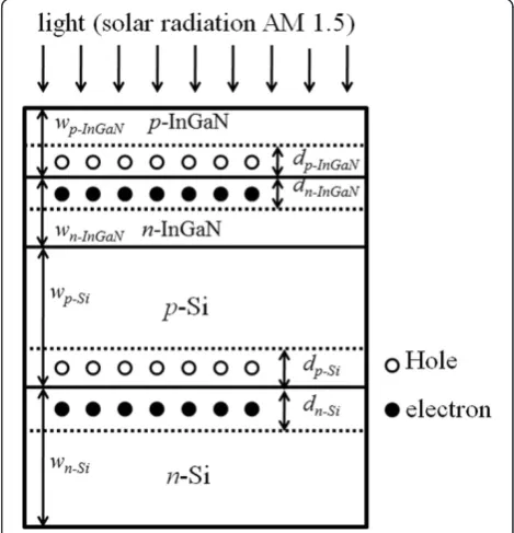
[image:2.595.304.539.422.666.2]Theoretical modeling of short circuit current density, open circuit voltage, fill factor, and conversion efficiency of InGaN/Si tandem cells
Figure 1 shows the structure of InGaN/Si tandem cells used for the theoretical simulation. wp-InGaN(−Si) and
wn-InGaN(−Si)are the thicknesses of the p- andn-InGaN (−Si) junctions, respectively.dp-InGaN(−Si)and dn-InGaN(−Si) are the thicknesses of the depletion region in thep- and
n-InGaN(−Si) junctions, respectively. The solar cells are under solar radiation AM 1.5G illumination (100 mW/ cm2). Photons are assumed to be incident from the
p-InGaN side of the InGaN top cell.
In the numerical simulations, the theoretical model is used to design the structures ofp-InGaN/n-InGaN/p-Si/
Figure 1The structure of InGaN/Si tandem cells used for theoretical simulation.Light (AM 1.5G illumination) is incident from thep-InGaN side.wp-InGaN(−Si)andwn-InGaN(−Si)are the thicknesses of thep- andn-InGaN(−Si) junctions, respectively.
n-Si tandem cells. Similar to the InGaN p-n junction solar cell in our previous study, the first-principles con-tinuity and Poisson’s equations are combined to analyze the transport behavior of the InGaN top cell and Si bot-tom cell [3,18]. The photovoltaic functions of the InGaN and Si subcells can be analyzed by solving a set of coupled differential equations for the electron density, hole density, and electrostatic potential [3,18]. Carrier and current densities can be analytically obtained to sep-arately determine the current-voltage (J-V) curves of the InGaN top cell and Si bottom cell.
The current density,JInGaN, in the InGaNp-njunction solar cells can be expressed as [3,18]:
JInGaN¼JSCPþJSCNþJG;D−ðJDPþJDNÞ
eqVa=kT−1
−JDD eqVa=2kT−1
ð1Þ
where JSCP is the hole diffusion current density in the
p-InGaN junction, JSCNis the electron diffusion current density in the n-InGaN junction, and JG,D is the drift current density in the depletion region.JDP,JDN,andJDD are the dark current densities in the p-InGaN junction,
n-InGaN junction, and depletion region, respectively.
Vais the built-in potential. Each term ofJSCP,JSCN,JG,D,
JDP,JDN, andJDDin Equation 1 can be obtained in refer-ences [3] and [18]. From Equation 1, JInGaN can be expressed as:
JInGaN¼Jsc−Js1 eqVa=kT−1
−Js2 eqVa=2kT−1
ð2Þ
Jsc≡JSCPþJSCNþJG;D ð3Þ
Js1≡JDPþJDN ð4Þ
Js2≡JDD ð5Þ
whereJSCis the photocurrent,Js1 eqVa=kT−1
is the dark current in the neutral region, and Js2 eqVa=2kT−1
is the recombination current in the depletion region. Details of the calculations of total current density, JInGaN, were described in references [3] and [18].
Similar to the InGaN p-n junction top cell, the first-principles continuity and Poisson’s equations are com-bined to analyze the transport behavior of the Si bottom cell [3,18]. The current density,JSi, in the Sip-njunction solar cells can be obtained [3,18].
The InGaN/Si tandem cell must consider the current-matching effect. The short circuit current density, Jsc, of an InGaN/Si tandem cell is limited by the smaller short circuit current density in the InGaN and Si subcells. It should be noted that the series and shunt resistances of the devices are not included in the following discussion in order to focus on the effects of the ideal diode charac-teristics of devices. However, it should be reminded that
in the cases of thick InGaN layers or poor metal contacts resulted from thep-doing InGaN, the effect of series resis-tances will become significant and their effects thus should be fully taken into account. In addition, the im-portant yet complicate issue regarding the tunnel junction is not discussed in this work; therefore, the tunnel junc-tion between the InGaN and Si is assumed to be an ideal one which has no additional effect on the devices’ per-formance. Of course, such an assumption is oversimpli-fied. Since the electron affinity of the InGaN varies widely with the indium composition, it is very difficult to achieve good tunnel junctions between the InGaN and Si and their effects on the devices’performance will be significant and thus deserve a separate and dedicate work to discuss this issue.
Assuming that the recombination current in the deple-tion region Js2 eqVa=2kT−1
≅0
is very small, the open-circuit voltage,Voc, can be obtained by setting theJInGaN in Equation 2 to be zero [3,18].
JInGaN¼Jsc−Js1 eqVa=kT−1
−Js2 eqVa=2kT−1
≈Jsc−Js1
eqVa=kT−1
≡0
ð6Þ
⇒Voc¼
kT q ln
JscþJs1
Js1 ð
7Þ
whenJsc> >Js1
⇒Voc≅
kT q ln
Jsc
Js1 ð
8Þ
The Voc of InGaN/Si tandem cell is the sum of the
Vocsof InGaN and Si subcells [3,18]. The fill factor, FF, is defined as:
FF¼ Pmax
Voc⋅Isc¼
Vmax⋅Imax
Voc⋅Isc ¼
Vmax⋅Jmax
Voc⋅Jsc ð
9Þ
The power conversion efficiency of a solar cell, η, is defined as [2,3]:
η¼Pmax
Pin ¼
FF⋅Voc⋅Isc
Pin ð
10Þ
The intrinsic carrier concentration,ni, can be described by [2,3]:
n2i ¼2:311031 mn⋅mp
m2 e
2=3
T3 exp − Eg
kT
ð11Þ
Egð Þ ¼x 0:65xþ3:425 1ð −xÞ−1:43xð1−xÞ ð12Þ
The absorption coefficients α(E) for direct InGaN and indirect Si as a function of energy, E, can be expressed as Equations 13 and 14, respectively,
αð Þ ¼E α0
ffiffiffiffiffiffiffiffiffiffiffiffiffiffiffiffiffiffiffi E−Egð Þx
Egð Þx
s
ð13Þ
αð Þ ¼E α0 E−Egð Þx Egð Þx
2
ð14Þ
whereEg(x) are the bandgaps of InxGa1-xN and Si [1]. The constant factorα0is shown in Table 1. Except for the bandgap energy, the physical parameters of InxGa1-xN are expressed as the linear interpolation formula of InN and GaN. The physical parameters of InN, GaN, and Si are listed in Table 1 [1,19-24]. Thep- andn-Si thicknesses are set at 0.7 and 200μm, respectively.
Operation mechanisms of InGaN p-n junction solar cells are explored through the calculation of characteris-tic parameters such as the Jsc,Voc, FF, and η. Two situa-tions are considered for theoretical simulation:
(I) Situation I: the dependence on the thickness (wp-InGaN = 50 to 4,000 nm) and the indium compos-ition (xp-InGaN= 0, 0.1….0.9, 1) of thep-InGaN junction. Then-InGaN thickness is set at 1,000 nm. The various thicknesses of thep-InGaN junction keep the depletion region of InGaN junction at the same distance from the
Si bottom subcell while changing the amount of light absorbed close to the depletion region of InGaN junction.
(II) Situation II: the dependence on the thicknesses (wn-InGaN= 50 to 4,000 nm) and the indium composition (xn-InGaN= 0, 0.1….0.9, 1) of the n-InGaN junction. The
p-InGaN thickness is set at 300 nm. The various thick-nesses of n-InGaN junction move the depletion region of InGaN junction relative to the Si bottom subcell while keeping the amount of light absorbed close to the deple-tion region of InGaN juncdeple-tion constant.
Results and discussion
(I) The effects of the thickness and the indium
composition of thep-InGaN junction on the performance of InGaN/Si tandem cells
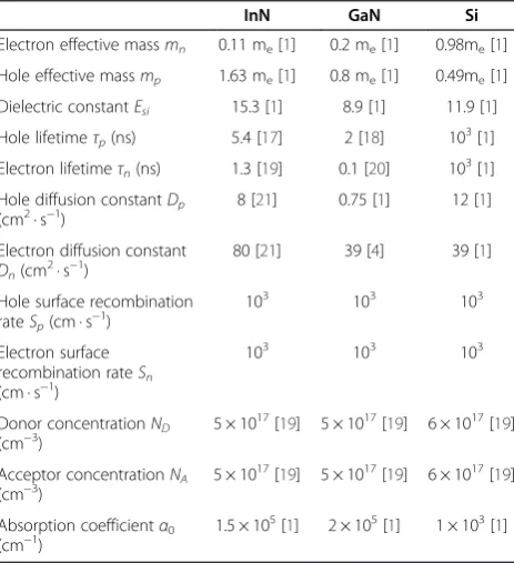
First, simulation I is conducted. Figure 2a shows the short circuit current density, Jsc(wp-InGaN, xp-InGaN), of InGaN/Si tandem cells as a function of p-InGaN thick-ness (wp-InGaN). The current-matching effect determines the behavior of theJsc. The discussions are divided into low- (xp-InGaN= 0 to 0.4), medium- (xp-InGaN= 0.5), and high-indium (xp-InGaN= 0.6 to 1.0) InGaN category regions:
(I) Forxp-InGaN= 0 to 0.4, theJscvery slightly increases and then drops with increasing wp-InGaN. The higher bandgap of the low-In InGaN results in the light passing through it being less absorbed. The Jsc of InGaN/Si tandem cells is the smaller of the InGaN subcell-limited photocurrents. Due to the photons being incident from thep-InGaN of the solar cell, photogenerated carriers in the p-InGaN contribute more photocurrent than those in then-InGaN. Aswp-InGaNincreases, a thickerwp-InGaN increases absorption. The Jsc very slightly increases. In addition, with a further increase inwp-InGaN(>1,000 nm), the depletion region of InGaN subcell is further away from the top cell surface. The collection efficiency of the minority carriers in the depletion region of InGaN subcell decreases and the probability of carrier recombination at surface defects increases. Thus, theJscdecreases.
(II) For xp-InGaN= 0.5, as the wp-InGaN increases, the Jsc slightly increases and then drops. With smaller (<400 nm), medium-sized (400 nm to 3 μm), and larger (>3 μm)
[image:4.595.58.290.479.733.2]wp-InGaN, theJscof an In0.5Ga0.5N/Si tandem cell is shown to be InGaN-, Si-, and InGaN subcell-limited, respectively. Two turning points, at current-matching condition around 400 nm and 3μm, are observed. (i) Forwp-InGaN< 400 nm, because the absorption coefficientα(hν)for solar cell mate-rials is finite, a cell of finite thickness will not absorb all the incident light above the bandgap. A thicker InGaN subcell increases the absorption and theJscslightly increases. Due to the medium bandgap, In0.5Ga0.5N (Eg= 1.68 eV) may not absorb so many photons such that theJscin the InGaN subcell is smaller than that in the Si subcell. The Jsc is InGaN-subcell-limited. (ii) With a further increase in
Table 1 The parameters of InN and GaN used for theoretical simulations
InN GaN Si
Electron effective massmn 0.11 me[1] 0.2 me[1] 0.98me[1]
Hole effective massmp 1.63 me[1] 0.8 me[1] 0.49me[1]
Dielectric constantEsi 15.3 [1] 8.9 [1] 11.9 [1]
Hole lifetimeτp(ns) 5.4 [17] 2 [18] 10 3
[1]
Electron lifetimeτn(ns) 1.3 [19] 0.1 [20] 10 3
[1]
Hole diffusion constantDp
(cm2· s−1) 8 [21] 0.75 [1] 12 [1] Electron diffusion constant
Dn(cm 2
· s−1)
80 [21] 39 [4] 39 [1]
Hole surface recombination rateSp(cm · s−1)
103 103 103
Electron surface recombination rateSn (cm · s−1)
103 103 103
Donor concentrationND (cm−3)
5 × 10¹⁷[19] 5 × 10¹⁷[19] 6 × 10¹⁷[19]
Acceptor concentrationNA
(cm−3) 5 × 10
17
[19] 5 × 10¹⁷[19] 6 × 10¹⁷[19]
Absorption coefficientα0 (cm−1)
wp-InGaNto (>400 nm), the lower transmission to the Si bottom subcell leads to the photocurrent in the Si subcell being lower than that in the InGaN subcell, so that theJscbecomes Si-subcell-limited. (iii) Forwp-InGaN>3μm, the depletion region of InGaN subcell is further away from the top cell surface. The collection efficiency of the mi-nority carriers in the depletion region of InGaN subcell decreases, and the probability of carrier recombination at surface defects increases. Hence, theJscdecreases and is again InGaN subcell-limited. Therefore, for the In0.5Ga0.5N/Si tandem cell, the thickness of the p-InGaN junction (wp-InGaN) should be adjusted to reapportion the light between the two subcells and to achieve the max-imum conversion efficiency.
(III) For xp-InGaN= 0.6 to 1.0, the Jscs are all the same and decrease with increasingwp-InGaN. A thickerwp-InGaN and the lower bandgap of the high-In InGaN top cell ab-sorbs more light, so less light is transmitted to the Si bot-tom cell. The photocurrent generated from the Si subcell becomes smaller and theJsc of the overall cell decreases further. TheJscs are Si subcell-limited.
Figure 2b shows the short circuit current density, Jsc (wp-InGaN,xp-InGaN), of InGaN/Si tandem cells as a func-tion of indium composifunc-tion (xp-InGaN). For the same thickness of p-InGaN, as the xp-InGaN increases, the Jsc increases and then decreases very slightly at a certain composition,xInGaN‐to‐Si
p−InGaN . It should be noted that once the
band-gap energy of the InGaN top subcell is smaller than that of the Si bottom subcell, the top cell will ab-sorb a certain potion spectrum of the incident photons which originally only can be absorbed by the Si bottom subcell. As a result, the short circuit current densities decrease very slightly for higher In compositions after reaching the maximum point. The respective low and
high absorptions of the low- xp−InGaN<xInGaNp−InGaN‐to‐Si
and high-In xp−InGaN>xInGaNp−InGaN‐to‐Si
InGaN lead to the
Jsc being InGaN and Si subcell-limited, respectively. As thewp-InGaNdecreases, thexInGaNp−InGaN‐to‐Sidecreases and then
increases. This is determined by the current-matching effect, as shown in Figure 2a.
[image:5.595.61.539.88.358.2]Figure 2c,d shows the open circuit voltage, Voc (wp-InGaN,xp-InGaN), of InGaN/Si tandem cells as a func-tion ofwp-InGaNandxp-InGaN, respectively. TheVocof an InGaN/Si tandem cell is equal to the sum of theVocs of the InGaN and Si subcells. In Figure 2c, except for the thicker cells, the Voc of an InGaN/Si tandem cell is nearly independent of thewp-InGaN. Note thatVocstarts to decrease slightly in the thicker cell, due to the larger saturation current, J0, in the thicker cell. In Figure 2d, becauseVocis determined by the bandgap energy of the subcell [18], smaller Vocin the high-In InGaN top cell is expected.
Figure 3a,b shows the fill factor, FF(wp-InGaN, xp-InGaN), of InGaN/Si tandem cells as a function of wp-InGaN and
xp-InGaN, respectively. The behaviors of FF are dramatic. According to Equations 9 and 10, the FF represents the combined effects ofPmax,Jsc, andVoc, which in turn are affected by the current-matching effect. Because the power maximum, Pmax, in Equation 10 is proportional to the conversion efficiency,η, the FF in Equation 9 rep-resents the ratio ofηto (Jsc*Voc). As shown in Figure 2c, except for the thicker wp-InGaN, the Voc of an InGaN/Si tandem cell is nearly independent of the wp-InGaN, the effect of Voccan be neglected and the FF represents the ratio of η to Jsc. In Figure 3a, the FFs are divided into low- (xp-InGaN= 0 to 0.4), medium- (xp-InGaN= 0.5), and high-indium (xp-InGaN= 0.6 to 1.0) InGaN categories:
(I) For xp-InGaN = 0 to 0.4, the FF are InGaN subcell-limited. Forxp-InGaN= 0, 0.1, and 0.2, as the wp-InGaN in-creases, the FF slightly increases and then decreases. For
xp-InGaN= 0.3 and 0.4, a minimum FF around 1 to 2 μm
wp-InGaNis observed.
(II) Forxp-InGaN= 0.5, the FF shows a dramatic variation with two minimums at current-matching condition around 400 nm and 3μm. With smaller (<400 nm), medium-sized (400 to 3,000 nm), and larger (>3μm)wp-InGaN, the FF of an In0.5Ga0.5N/Si tandem cell is shown to be InGaN-, Si-, and InGaN subcell-limited, respectively. Because Jsc has two turning points around 400 nm and 3 μm, two mini-mum FF at current-matching condition are expected.
(III) For xp-InGaN= 0.6 to 1.0, the FF are Si subcell-limited. As the wp-InGaN increases, the FF increases and then decreases at 1 to 2μm.
In Figure 3b, the FFs for low- xp−InGaN<xInGaNp−InGaN‐to‐Si
and high-In xp−InGaN>xInGaNp−InGaN‐to‐Si
InGaN/Si tandem
cells are InGaN and Si subcell-limited, respectively. Minimum FF at the current-matching condition is ob-served at a certain composition,xInGaNp−InGaN‐to‐Si. ThexInGaNp−InGaN‐to‐Si
is also determined by the same xInGaN‐to‐Si
p−InGaN , as shown in
Figure 2b. In general, the III-V solar cells exhibit a high FF of 0.80 to 0.86 [25]. Without consideration of the effects of the current leakage and shunt resistance, the simulation results of FF can be higher than those of the actual fabri-cated solar cells.
Figure 3c,d shows the conversion efficiency,η(wp-InGaN,
xp-InGaN), of an InGaN/Si tandem cell as a function of
wp-InGaNandxp-InGaN, respectively. Simulation results help us to better understand the current-matching effect and operation mechanisms in and provide the optimized structure design of InGaN/Si tandem cells. The η repre-sents the combined effects of Jsc,Voc, and FF, which in turn are affected by the current-matching effect.
In Figure 3c, the trend of ηis similar to that of Jsc in Figure 2a. This shows that Jsc is a dominant factor in determining the performance of InGaN/Si tandem cells. Theηis divided into low- (xp-InGaN= 0 to 0.4),
medium-Figure 3Fill factor.FF(wp-InGaN,xp-InGaN) of InGaN/Si tandem cells as a function ofp-InGaN(a)thickness,wp-InGaNand(b)indium composition,
[image:6.595.60.538.435.704.2](xp-InGaN= 0.5), and high-indium (xp-InGaN= 0.6 to 1.0) InGaN categories:
(I) For xp-InGaN= 0 to 0.4, the InGaN subcell-limited η slightly increases and then drops with increasingwp-InGaN. Due to very lowerη, low-indium content (xp-InGaN= 0 to 0.3) InGaN/Si tandem cells are not suitable for application in solar cells.
(II) For xp-InGaN= 0.5, as the wp-InGaN increases, the
η slightly increases and then drops. With smaller (<400 nm), medium-sized (400 to 3,000 nm), and larger (>3μm)wp-InGaN, theηis shown to be InGaN-, Si-, and InGaN subcell-limited, respectively. Two turning points at current-matching condition around 400 nm and 3 μm are observed. The current-matching effect deter-mines the behavior of the η. With 100 to 300 nm
p-InGaN and 300 nmn-InGaN, the In0.5Ga0.5N(1.68 eV)/ Si(1.12 eV) tandem cell can exhibit as high aηas approxi-mately 34%.
For xp-InGaN= 0.6 to 1, the Si subcell-limited η de-creases with increasing wp-InGaN. With 50 nm p-InGaN and 300 nm n-InGaN, the In0.6Ga0.4N(1.42 eV)/Si (1.12 eV) tandem cell can exhibit as high aηas mately 36.5%, which is much higher than the approxi-mately 22% conversion efficiency of an In0.6Ga0.4N p-n
single junction solar cell and comparable to the 35% to 38% conversion efficiency of a GaInP(1.95 eV)/GaAs (1.42 eV) tandem cell [3,13].
In Figure 3d, the combined effects of theJsc,Voc, and FF lead to an optimizedηin the medium-indium,xInGaN‐to‐Si
p−InGaN ,
InGaN/Si tandem cell. AtxInGaNp−InGaN‐to‐Si, theJscof the InGaN subcell is equal to that of the Si subcell such that the InGaN/Si tandem cell reaches the current matching con-dition to operate at the maximum power point. Similar to
Jsc and FF, the η for low- xp−InGaN<xInGaNp−InGaN‐to‐Si
and
high-In xp−InGaN>xInGaNp−InGaN‐to‐Si
InGaN/Si tandem cells
are InGaN and Si subcell-limited, respectively. The
xInGaN‐to‐Si
p−InGaN in Figure 3d is the same as the xInGaNp−InGaN‐to‐Si in
Figure 2b. With 100 nm p-InGaN and 300 nm n
-InGaN, the In0.55Ga0.45N(1.54 eV)/Si(1.12 eV) tandem cell can exhibit as high a η as approximately 36.5%, which is much higher than approximately 22% conver-sion efficiency of an In0.6Ga0.4N p-n single junction solar cell and comparable to the 35% to 38% conversion efficiency of GaInP(1.95 eV)/GaAs(1.42 eV) tandem cell [3,13]. This demonstrates that the medium-indium InGaN/Si tandem cell is an appealing candidate to realize a high-efficiency solar cell. However, the diffi-culty of high-quality devices would be a potential obstacle to fabricating such tandem cells. Growth of In-rich InGaN can be obtained by using high-pressure chemical vapor deposition [26,27].
(II) The effects of the thickness and the indium
composition of then-InGaN junction on the performance of InGaN/Si tandem cells
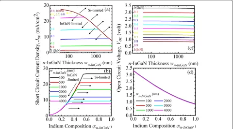
Secondly, simulation II is conducted. Figure 4a,b shows the short circuit current densities,Jsc(wn-InGaN, xn-InGaN), of InGaN/Si tandem cells as a function of n-InGaN thickness (wn-InGaN) and indium composition (xn-InGaN), respectively. In Figure 4a, current-matching effect cate-gorizes the Jsc into InGaN and Si subcell-limited areas. The discussions are divided into low- (xn-InGaN= 0 to 0.2), medium- (xn-InGaN= 0.3 to 0.5), and high-indium (xp-InGaN= 0.6 to 1) InGaN regions:
(I) Forxn-InGaN= 0 to 0.2, theJscslightly increases with increasing wn-InGaN, due to the increase of photon ab-sorption by thickern-InGaN layer. The higher bandgap of the low-In InGaN results in the light passing through it being less absorbed. TheJscis InGaN subcell-limited.
(II) For xn-InGaN= 0.3 to 0.5, as the wn-InGaN increases, theJscslightly increases and then drops beyond a certain thickness wInGaN‐to‐Si
n−InGaN
. The current-matching effect cat-egorizes the Jsc into InGaN and Si subcell-limited areas. A largerwn-InGaNabsorbs more photons such that theJsc slightly increases. As the wn-InGaN is beyond a certain thickness wInGaNn−InGaN‐to‐Si, the enhanced absorption of n -InGaN leads to less light being transmitted to the Si bot-tom subcell. TheJscis Si subcell-limited. Also, the higher thexn-InGaN, the smaller thewInGaNn−InGaN‐to‐Sican be. Due to the lower bandgap of the high-In InGaN, a smaller w n-InGaN can absorb more photons to reach the current-matching condition.
(III) Forxp-InGaN= 0.6 to 1, theJscs are all the same and decrease with increasing wn-InGaN. A thicker wn-InGaN, combined with the low bandgap of high-In InGaN, ab-sorbs more photons and leads to less transmittance to the Si bottom subcell. The photocurrent generated from the Si subcell becomes smaller and the Jsc of the overall cell decreases further. TheJscis Si subcell-limited.
In Figure 4b, as thexn-InGaNincreases, theJscincreases and thendecreases very slightlyat a certain composition,
xInGaNn−InGaN‐to‐Si, at which theJscceases to increase. Similar to the Jsc(wp-InGaN, xp-InGaN) in Figure 2b, the current-matching effect can also explain the trend ofJsc(wn-InGaN,
xn-InGaN). Also, the thinner the wn-InGaN, the higher the indium composition, xInGaN‐to‐Si
n−InGaN , to reach the current
matching condition. The thickness and bandgap of the
n-InGaN layer can determine the light flux reaching the Si subcell. With a thinnerwn-InGaN, more light is able to reach the Si subcell to generate more photocurrent. The
from InGaN to Si subcell-limited is observed at a higher indium composition.
Figure 4c,d shows the open circuit voltage,Voc(wn-InGaN,
xn-InGaN), of InGaN/Si tandem cells as a function of
wn-InGaN and xn-InGaN, respectively. The trend of Voc (wn-InGaN, xn-InGaN) is similar to that of Voc(wp-InGaN,
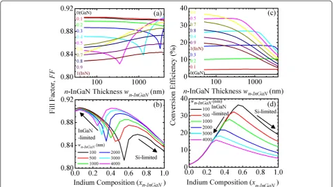
xp-InGaN). A similar argument can explain this trend. Figure 5a,b shows the fill factor, FF(wn-InGaN, xn-InGaN), of InGaN/Si tandem cells as a function ofwn-InGaN and
xn-InGaN, respectively. Similar to the previous argument, the FF represents the ratio ofη to Jsc. In Figure 5a, the FF is divided into low- (xn-InGaN= 0 to 0.2), medium-(xn-InGaN= 0.3 to 0.5), and high-indium (xp-InGaN= 0.6 to 1) InGaN categories:
(I) For xn-InGaN= 0 to 0.2, as the wn-InGaN increases, the InGaN subcell-limited FF slightly decreases.
(II) Forxn-InGaN= 0.3 to 0.5, as thewn-InGaNincreases, the FF decreases and then dramatically increases. Forwn−InGaN
<wInGaN‐to‐Si
n−InGaN andwn−InGaN>wInGaNn−InGaN‐to‐Si, the FF of InGaN/
Si tandem cells are InGaN and Si subcell-limited, respect-ively. For each composition, minimum FF at the current-matching condition is observed at the wInGaN‐to‐Si
n−InGaN . This
wInGaN‐to‐Si
n−InGaN is the same aswInGaNn−InGaN‐to‐Sishown in Figure 4a.
(III) For xn-InGaN= 0.6 to 1, as the wn-InGaN increases, the Si subcell-limited FF increases.
In Figure 5b, for xn−InGaN≤xInGaNn−InGaN‐to‐Si
and
xn−InGaN≥xInGaNn−InGaN‐to‐Si
, the FF of InGaN/Si tandem cells
are InGaN and Si subcell-limited, respectively. As the
xn-InGaN increases, minimum FF at the current-matching condition is observed at a certain composition,xInGaNn−InGaN‐to‐Si. ThexInGaN‐to‐Si
n−InGaN is also determined by the samexInGaNn−InGaN‐to‐Si,
as shown in Figure 4b.
Figure 5c,d shows the conversion efficiency, η(w n-InGaN, xn-InGaN), of InGaN/Si p-n tandem cells as a function of wn-InGaN and xn-InGaN, respectively. Theηis determined by the current-matching effect. In Figure 5c, the trend of ηis similar to that ofJsc in Figure 4a. This shows that Jsc is a dominant factor in determining the performance of InGaN/Si tandem cells. Theηare divided into low- (xn-InGaN= 0 to 0.2), medium- (xn-InGaN= 0.3 to 0.5), and high-indium (xp-InGaN= 0.6 to 1) InGaN categories:
(I) For xn-InGaN= 0 to 0.2, the InGaN subcell-limitedη is slightly higher in the thicker wn-InGaN tandem cells. Thisηis lower than that of Si solar cell. This shows that the low-indium InGaN/Si tandem cell is not suitable for solar cell applications.
(II) For xn-InGaN= 0.3 to 0.5, as the wn-InGaN increases, theηslightly increases and then drops at thewInGaNn−InGaN‐to‐Si. For each composition, maximum η at the current-matching condition is observed at the wInGaN‐to‐Si
n−InGaN . With
wn−InGaN<wInGaNn−InGaN‐to‐Si and wn−InGaN>wInGaNn−InGaN‐to‐Si, the η
[image:8.595.58.539.90.357.2]of InGaN/Si tandem cells are InGaN and Si subcell-limited, respectively. With 300 nmp-InGaN and 100 to
Figure 4Short circuit current density.Jsc(wn-InGaN,xn-InGaN) of InGaN/Si tandem cells as a function ofn-InGaN(a)thickness,wn-InGaN, and
300 nm n-InGaN, the In0.5Ga0.5N(1.68 eV)/Si(1.12 eV) tandem cell can exhibit as high aηas approximately 34%.
(III) For xn-InGaN= 0.6 to 1, the Si subcell-limited ηis lower in the thicker wn-InGaN InGaN/Si tandem cells.
With 300 nm p-InGaN and 50 nm n-InGaN, the
In0.6Ga0.4N(1.42 eV)/Si(1.12 eV) tandem cell can exhibit as high a η as approximately 36.5%, which is much higher than the approximately 22% conversion efficiency of an In0.6Ga0.4Np-nsingle junction solar cell and com-parable to the 35% to 38% conversion efficiency of a GaInP(1.95 eV)/GaAs(1.42 eV) tandem cell [3,13].
In Figure 5d, as the xn-InGaN increases, the trends of
Jsc, Voc, and FF lead to the maximum η in the medium-In, xInGaNn−InGaN‐to‐Si, InGaN/Si tandem cells. At
xInGaN‐to‐Si
n−InGaN , the Jsc of the InGaN subcell is equal to
that of the Si subcell such that the current-matching condition is obtained for the InGaN/Si tandem cell operating at the maximum power point. Similar to Jsc and FF, theηfor low- xn−InGaN<xInGaNn−InGaN‐to‐Si
and high-In
xn−InGaN>xInGaNn−InGaN‐to‐Si
InGaN/Si tandem cells are InGaN and Si subcell-limited, respectively. The In composition corresponding to the optimized η is the same as the
xInGaN‐to‐Si
n−InGaN shown in Figure 4b. With 300 nmp-InGaN and
100 nmn-InGaN, the In0.55Ga0.45N (1.54 eV)/Si (1.12 eV) tandem cell has the maximum η approximately 36.5%. The xInGaN‐to‐Si
n−InGaN for the maximumηis determined by the
current-matching effect.
Conclusions
In summary, we have shown that the performance and characteristics of the InGaN/Si tandem cells are deter-mined by the current-matching effect, which in turn is af-fected by thep-andn-layer thicknesses, indium content, and position of depletion region of the InGaN subcell.Jsc is a dominant factor in determining the performance of InGaN/Si tandem cells. The combined effects of the Jsc,
Voc, and FF lead to an optimizedηin the medium-indium content, xInGaN‐to‐Si
p nð Þ−InGaN, InGaN/Si tandem cell. Similar toJsc and FF, the η for low- xp nð Þ−InGaN<xInGaNp nð Þ−InGaN‐to‐Si
and
high-In xp nð Þ−InGaN>xInGaNp nð Þ−InGaN‐to‐Si
InGaN/Si tandem cells
are InGaN- and Si subcell-limited, respectively. With ap-propriate thicknesses ofp- andn-InGaN, In0.5–0.6Ga0.5–0.4 N/Si tandem cells can exhibit as high as approximately 34% to 36.5% conversion efficiency. The performance of InGaN/Si tandem cells can be optimized through the optimization of the device structures. Simulation results help us to better understand the current-matching effect and operation mechanisms of InGaN/Si tandem cells.
Competing interests
The authors declare that they have no competing interests.
Authors’contributions
[image:9.595.56.540.89.360.2]CML prepared the theoretical formula and did the theoretical simulation. CYT and LWT made result discussions. SWF coordinated the project and drafted the paper. All the authors read and agree the final version of the paper.
Figure 5Fill factor, FF(wn-InGaN,xn-InGaN).Of InGaN/Si tandem cells as a function ofn-InGaN(a)thickness,wn-InGaN, and(b)indium composition,
Acknowledgement
This research was supported by the Ministry of Science and Technology, Taiwan, R.O.C., under grants NSC 100-3113-E-110-004, NSC 99-2112-M-390-002-MY3, and NSC 99-2515-S-390-001.
Author details
1Department of Applied Physics, National University of Kaohsiung, Kaohsiung, Taiwan.2Department of Electronic Engineering, Ming Chuan University, Taoyuan, Taiwan.3Department of Physics and Center for Nanoscience and Nanotechnology, National Sun Yat-Sen University, Kaohsiung, Taiwan.
Received: 10 October 2014 Accepted: 18 November 2014 Published: 2 December 2014
References
1. Schubert EF:Light Emitting Diodes.Cambridge: Cambridge University Press; 2006.
2. Feng SW, Lai CM, Chen CH, Sun WC, Tu LW:Theoretical simulations of the
effects of the indium content, thickness, and defect density of thei-layer on the performance ofp-i-nInGaN single homo-junction solar cells.
J Appl Phys2010,108:093118.
3. Feng SW, Lai CM, Tsai CY, Su YR, Tu LW:Modeling of InGaNp-njunction
solar cells.Opt Mater Express2013,3:1777–1788.
4. Jani O, Ferguson I, Honsberg C, Kurtz S:Design and characterization of GaN/InGaN solar cells.Appl Phys Lett2007,91:132117.
5. Lang JR, Neufeld CJ, Hurni CA, Cruz SC, Matioli E, Mishra UK, Speck JS:High external quantum efficiency and fill-factor InGaN/GaN heterojunction solar cells grown by NH3-based molecular beam epitaxy.Appl Phys Lett 2011,98:131115.
6. Zheng X, Horng RH, Wuu DS, Chu MT, Liao WY, Wu MH, Lin RM, Lu YC:
High-quality InGaN/GaN heterojunctions and their photovoltaic effects.
Appl Phys Lett2008,93:261108.
7. Cai XM, Zeng SW, Zhang BP:Fabrication and characterization of InGaN
p-i-nhomojunction solar cell.Appl Phys Lett2009,95:173504. 8. Jampana BR, Melton AG, Jamil M, Faleev NN, Opila RL, Ferguson IT,
Honsberg CB:Design and realization of wide-band-gap (~2.67 eV) InGaN
p-njunction solar cell.IEEE Electron Device Lett2010,31:32–34. 9. Dahal R, Li J, Aryal K, Lin JY, Jiang HX:InGaN/GaN multiple quantum well
concentrator solar cells.Appl Phys Lett2010,97:073115.
10. Fujii T, Kuwahara Y, Iida D, Fujiyama Y, Morita Y, Sugiyama T, Isobe Y, Iwaya M, Takeuchi T, Kamiyama S, Akasaki I, Amano H:GaInN-based solar cells using GaInN/GaInN superlattices.Phy Status Solidi C2011,8:2463.
11. Feng SW, Chen YY, Lai CM, Tu LW, Han J:Anisotropic strain relaxation and the resulting degree of polarization by one- and two-step growth in nonpolara-plane GaN grown onr-sapphire substrate.J Appl Phys2013, 114:233103.
12. Feng SW, Yang CK, Lai CM, Tu LW, Sun Q, Han J:Surface striation, anisotropic in-plane strain, and degree of polarization in nonpolar
m-plane GaN grown on SiC.J Phys D Appl Phys2011,44:375103. 13. Luque A, Hegedus S:Chapter 8 in Handbook of Photovoltaic Science and
Engineering.Chichester: John Wiley & Sons; 2011.
14. Yamamoto A, Islam MR, Kang TT, Hashimoto A:Recent advances in
InN-based solar cells: status and challenges in InGaN and InAlN solar cells.Phys Status Solidi C2010,7:1309.
15. Zhang XB, Wang XL, Xiao HL, Yang CB, Ran JX, Wang CM, Hou QF, Li JM,
Wang ZG:Theoretical design and performance of InxGa1-xN two-junction solar cells.J Phys D Appl Phys2008,41:245104.
16. Hsu L, Walukiewicz W:Modeling of InGaN/Si tandem solar cells.J Appl Phys2008,104:24507.
17. Shen XB, Lin S, Li F, Wei Y, Zhong S, WaN H, Li J:Simulation of the InGaN-based tandem solar cells.Proc of SPIE2008,7045:70450E. 18. Nelson J:Chapter 6 in The Physics of Solar Cells.London: Imperial College
Press; 2003.
19. Zhang XB, Wang XL, Xiao HL, Yang CB, Ran JX, Wang CM, Hou QF, Li JM:
Simulation of In0.65Ga0.35N single-junction solar cell.J Phys D Appl Phys 2007,40:7335.
20. Chen F, Cartwright AN:Hole transport and carrier lifetime in InN epilayers.Appl Phys Lett2005,87:212104.
21. Shur MS, Davis RF:GaN-Based Materials and Device.Singapore: World Scientific; 2004.
22. Chena F, Cartwright AN, Lu H, Schaff WJ:Temperature-dependent optical
properties of wurtzite InN.Phys E2004,20:308–312.
23. Bandic ZZ, Bridger PM, Piquette EC, McGill TC:Electron diffusion length and lifetime inp-type GaN.Appl Phys Lett1998,73:3276–3278.
24. Brown GF, Ager JW III, Walukiewicz W, Wu J:Finite element simulations of compositionally graded InGaN solar cells.Sol Energy Mater Sol Cells2010, 94:478–483.
25. Green MA, Emery K, Hishikawa Y, Warta W, Dunlop ED:Solar cell efficiency tables.Prog Photovolt Res Appl2013,21:827–837.
26. Iida D, Nagata K, Makino T, Iwaya M, Kamiyama S, Amano H, Akasaki I,
Bandoh A, Udagawa T:Growth of GaInN by raised-pressure metalorganic
vapor phase epitaxy.Appl Phys Exp2010,3:075601.
27. Durkaya G, Alevli M, Buegler M, Atalay R, Gamage S, Kaiser M, Kirste R, Hoffmann A, Jamil M, Ferguson I, Dietz N:Growth temperature-phase stability relation in In1-xGaxN epilayers grown by high-pressure CVD.
Mater Res Soc Symp Proc2010,1202:1202–I5.21.
doi:10.1186/1556-276X-9-652
Cite this article as:Fenget al.:Numerical simulations of the
current-matching effect and operation mechanisms on the performance of InGaN/Si tandem cells.Nanoscale Research Letters20149:652.
Submit your manuscript to a
journal and benefi t from:
7Convenient online submission 7Rigorous peer review
7Immediate publication on acceptance 7Open access: articles freely available online 7High visibility within the fi eld
7Retaining the copyright to your article