ISSN: 1992-8645 www.jatit.org E-ISSN: 1817-3195
NOVEL TECHNIQUE TO ENHANCE SECURITY OF
RECONFIGURABLE CIRCUITS
1BINU K. MATHEW, 2Dr. K. P. ZACHARIA
1
Research Scholar, Anna University, Chennai, Tamil Nadu, INDIA
2
Professor, SAINTGITS College of Engineering, Kottayam, Kerala, INDIA
E-mail: [email protected], [email protected]
ABSTRACT
FPGAs are used in various applications like aero-space, automotive, military etc which require them to operate in different types of environments. Security of FPGA based system is a big concern as the system developed after lot of research can be stolen very easily. Nowadays, a lot of research is going on, considering various security aspects of FPGAs as the primary concern. Several cryptographic systems are available which can be used to protect FPGA bit-streams. Cryptographic techniques are used to encrypt the FPGA bit-streams. It is not feasible to use FPGAs in small circuit as it increase cost of the system under consideration. This paper proposes a technique which makes a digital system secure by using look-up tables. Behavior of a look-up table is based on its configuration bit. Look-up tables can be used to replace a digital circuit either fully or partially. If a look-up table replaces the whole circuit, then it can be called as fully incomplete and if the look-up table replaces only a part of a digital circuit, then that circuit can be called as partially incomplete. Digital systems can be made secure by fully incomplete design or partially incomplete design. Fully incomplete design can be used in the case of small circuits and for complex circuits a portion of the design can be made incomplete, in the case of partially incomplete digital circuits. This paper proposes a novel technique to enhance security of reconfigurable circuit. An authorized user completes the design of the circuit at run time by entering the configuration bits of the look-up table.
Keywords - FPGAs, Secure devices, Volatile devices, Look-up Table, Multi-functional chips
1. INTRODUCTION
Applications Field Programmable Gate Arrays are logic devices that consist of logic modules and a programmable interconnection network which is an alternative to costly ASIC based systems. FPGAs play a vital role in the day to day life of human being like national infra structure, transportation, military and medical areas. Advanced features of FPGAs give rise to some security treats to FPGA based system. A design is an intellectual property of a designer, who has invested lot of resources, which should be protected from cloning and unauthorized usage [3], [4], [5] and [6]. Researchers has proposed several possible attacks against FPGAs, including modifying the hardware, extracting other information through physical side channels, changing the functionality through design tools and cloning of IP core developed by a manufacturer. [5], [6]. Several cryptographic algorithms are proposed in [7] - [9] to reduce the effort of bit-stream copying. Cryptographic algorithms are applicable only to programmable devices like FPGAs, and not feasible for simple systems which are prone to copying of design. A
The remainder of this paper is organized as follows. Previous work is discussed in Section 2. In Section 3, we present a Binary Key Multiplexed Logic Module that can be used as a multi-functional device for the development of run time reconfigurable. Section 4 explains how the proposed system is secure. In Section 5, an implementation case study is presented and experimental results are discussed in Section 6. At last Concluding remarks are presented in Section 7.
2. PREVIOUS WORK
A novel technique to implement a logic circuit using 3-LUT which can be used to make a FPGA based system secure is discussed in [1, 2]. There are various threat models for FPGA based system like copying of bit-streams, Trojan attacks etc. These threat models discuses the way in which FPGA based systems are affected. Various security concerns in SRAM based volatile FPGA is discussed in [3]. Various techniques for bit-stream authentication are discussed in detail by S. Drimer in [4]. The techniques discussed in [4] give an insight to securing a design of FPGA based system which alleviates the possibility of copying of the bit-streams. The security related issues in reconfigurable systems for sensitive applications, various possible attacks and solutions to these problems are addressed in [5]. The topics of trusted hardware, design theft physical attacks and system security are also addressed in [5]. In [6], a system is designed to evaluate the security aspects of a reconfigurable hardware. This paper in [6] proposes a separation technique which ensures that reference monitor is tamper proof and cannot be bypassed. Programmability of FPGA is a major advantage for providing on-chip security to incorporate self-protective security mechanisms at a much lower
cost [7]. Several types of crypto processors and their applications are surveyed in rapidly developing area. Power analysis, Emission attack and Logical attack some of the areas where high end systems remain weak area [8]. A new approach to Digital Rights Management by combining directed NBTI aging and delay logic I proposed in [9]. Several rapidly evolving pre-fabricated FPGA architecture are discussed in [10]. This includes asynchronous and nano technology architectures. In [11] architecture of a secured reconfigurable system-on-programmable chip is discussed which explain a computer system made on a SoPC. Implementation of a unique chip ID for polymorphic circuit which is reconfigurable is discussed in [12]. Apart from the conventional threat models, new threats for security of integrated circuit and its solution are discussed in [13]. Several possible threats that may occur during the IC fabrication process and architecture of a reconfigurable logic barrier are discussed in [14]. Several techniques are discussed by the authors in [15] which includes encapsulation, dongle, manufacturer defined key etc. In [16] author proposes a secure computing module which provides data security and protection against malicious attack. The system is strongly based on encryption algorithms like AES algorithm. Some security threats in ICs and hardware assurance counter measures are discussed in [17].
3. PROPOSED SYSTEM
ISSN: 1992-8645 www.jatit.org E-ISSN: 1817-3195
Figure1 3 Input - LUT Implements A Different Function with Different Configuration Bits
3.1 Introduction
The reconfigurable elements used in reconfigurable devices like FPGA are multiplexers. We know that a multiplexer can be used to implement different logic functions. A 4:1or 22:1 multiplexer with two select lines can be used to implement 2 variable functions, 23:1 multiplexer can be used to implement a 3 variable function and in general a 2N:1 multiplexer can be used to implement an N-variable function. The binary value given at the input of a multiplexer can be considered as the control word to implement a function. For example, for a multiplexer with three select lines, the number of input lines is 8, and let the 8 bit binary value at the input of the multiplexer is 00100110. The output of the multiplexer is logic ‘1’ if and only if the select lines are loaded with 101, 010 or 001, in other words the multiplexer realizes the 3 variable function AB’C + A’BC’ +A’B’C. The functionality of this multiplexer can be changed if the binary input is changed to a 00010001, the multiplexer realize the logic function AB’C’ + A’B’C’. In other words, logic module can be re-configured by changing the binary value at the multiplexer input. As shown in Fig. 1, functionality of a look-up table can be changed by changing the binary values at the input lines of the look-up table. For this reason this binary value can be called as the control word of the multiplexer. The logic module can be reconfigured at any time by changing the control word given to the multiplexer input. Systems designed using Logic Module behaves in a different way when the control word is changed. For example, for the above 3 input logic module, if the control word is 10000011, the function Z=A’B’C’+A’B’C+ABC is
realized and with a new control word like 10000000, the logic module realize the function Z=ABC.
of eight different functions can be loaded into the proposed system one after another with PGM input set as logic’1’. In function mode PGM is set as
logic ‘0’ and FUN_ID bits are placed on the FUN_ID bus.
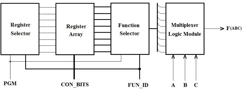
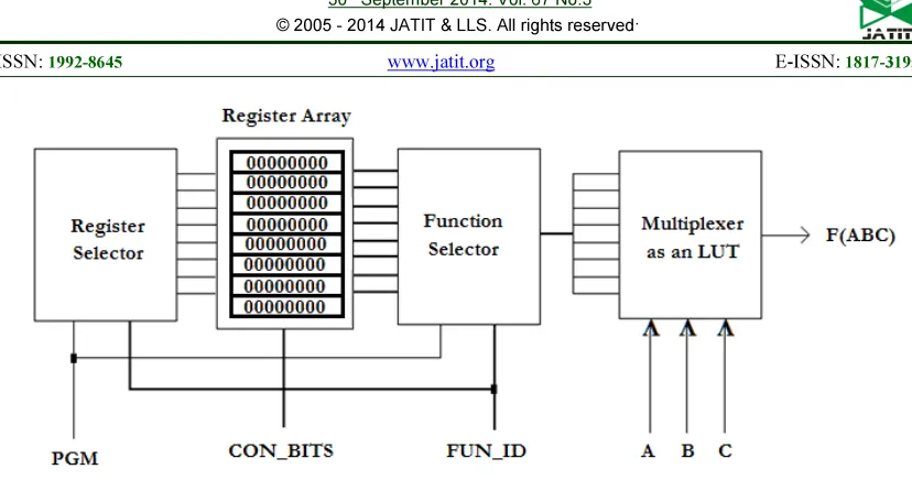
[image:4.595.100.495.181.327.2]Figure2 Block diagram of a Secured Multi Functional Chip (BKM-LM)
Figure 3 Various Blocks of BKM-LM (a) Register Selector Block (b) Register Array Block (c)Function Selector Block and (d) Multiplexer Logic Module Block
3.2 Register Selector Block
A Register selector block (RSB) which is basically a N: 2N decoder comes into play when the logic module is in program mode. In program mode, the program input ‘PGM’ is set as ‘1’ and this enables the register selector block. Based on the binary value placed at the FUN_ID, one of the M bit register in the register bank receives a clock,
ISSN: 1992-8645 www.jatit.org E-ISSN: 1817-3195
which is basically a decoder which decodes the address placed on the FUN_ID of BKM-LM giving clock signal to load a control word placed on the CON_BITS inputs of the BKM-LM.
3.3 Register Array Block
The register array block which is basically an array of D Flip Flops consists of N-bit registers of length M. Value of N depends on number of variables in the function to be implemented. Length of the array depends on the number of functions implementable in the logic module. For example if a user wants to implement 8 four variable functions, value of N must be four and that of M must be eight. To implement more number of functions with more number of input variable, the length of the D flip flop array should be increased, which increases the complexity of the system. Fig 3(b) shows the block diagram of a Register Array Block (RAB). The control word is placed on the input Din of the Register Array Block (RAB) and a clock signal is applied to that register where these control word is to be latched. The latched control word is available at the output of each register. The content of a register can be altered by placing the new binary value at the input of the Register Array Block and placing logic ‘1’ at the clock input of that register. The new value is loaded in to the register location which received a positive clock on its input.
3.4 Function Selector Block
Function Selector Block (FSB) is used to select one function from a set of functions. Function Selector Block is basically an M: 1 multiplexer of width N which selects the bit-stream of a particular function to be implemented. As shown in Fig 3(c), this part of the system makes the system a multi-functional one. The number of input channels of the Function Selector Block (FSB) determines the number of functions that can be implemented by the system. If the number of channels is M and if the width of a channel is 2N, the function can implement M different functions with N variables. To implement a multi-functional device this can implement 16 functions with 3 variables, Function
Selector Block must be 8 bit (23) wide, 16:1 multiplexer. FUN_ID is placed on the address bus (select lines of the multiplexer) of the FSB which selects one function out of M different functions. The FSB is disabled when the BKM-LM is in program mode and it is enabled only in the function mode.
3.5 Multiplexer As Logic Module
A multiplexer is used as a reconfigurable element in most of the programmable devices like FPGAs. In the proposed system also, a multiplexer is used as the programmable element. Multiplexer is used to realize a function and complexity of the function depends on the number of input channels of the multiplexer. For a multiplexer with 2N input channels can realize a function with ‘N’ number of variables. An 8:1 multiplexer can realize a 3 variable function and to realize a 4 variable function, a 16:1 multiplexer is needed. Fig 3(d) shows use of an 8:1 multiplexer or 3 variable look-up tables as a logic module. Function Selector Block selects a control word from several control words based on the binary value at the FUN_ID. By changing the FUN_ID, control word and thus functionality of the multiplexer can be changed.
4. HOW THE PROPOSED SYSTEM IS SECURE?
Let us discuss the security aspects of a circuit realized using Logic Module. For a combinational circuit with three variables, there are several possible control words and the device performs the intended function if and only if the proper control word is applied. Functionality of the proposed system depends on the control word loaded from register array to input of the multiplexer. For a multiplexer based logic module with N input variables, number of input lines is 2N, i.e., total number of bits in the control word is 2N
Figure 4: Status of Registers in Register Array Block Initially – All Locations filled with “00000000”
Figure 5: Registers in the Register Array Block is loaded with Several Configuration Bits
When number of input variables becomes four, the number of select lines becomes N = 4 and total number of input lines for the multiplexer is M=24 = 16 and total number of functions by this multiplexer as a look-up table is 216 = 512, i.e., when number of select lines of a multiplexer rises by one, number of locations in the look-up table doubles. Fig. 4 shows that the Register Array Block (RAB) is loaded with 0s by default and the user loads various control words into the RAB at run time based on the functionality required, as shown in Fig. 5. The attacker or intruder may not know whether he is using the logic module based system with its intended functionality or not. A designer who doesn’t want to reveal design details of the heart of his system can use control word based system. The system performs the intended function
[image:6.595.105.501.353.520.2]ISSN: 1992-8645 www.jatit.org E-ISSN: 1817-3195
Figure 6: Full implementation of the function F=ABC’+A’BC+A’B’C’
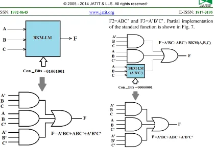
5. MOTIVATIONAL EXAMPLE
Let us consider one standard function from thirteen standard functions discussed by authors in [19], A’BC+ABC’+A’B’C’, which is used in some logic system. A FPGA can be used to implement this function which increases system complexity and cost. The same function can be implemented using the proposed system with less complexity and cost. As proposed in this paper, the above function can be implemented either fully or partially. For full implementation of this function using the proposed system, the configuration bit stream for the system is “01001001”. The full implementation of the standard function is shown in Fig. 6. The function under consideration can be implemented partially by using the proposed system as discussed below. The function F = A’BC+ABC’+A’B’C’, can be written as F = F1+F2+F3, where F1, F2 and F3 are components of F and given as F1=A’BC,
F2=ABC’ and F3=A’B’C’. Partial implementation of the standard function is shown in Fig. 7.
Figure 7: Partial implementation of the function F=ABC’+A’BC+A’B’C’
[image:7.595.91.512.91.382.2]Figure 8: Implementation of the function F=ABC+A’BC+A’BC’
In message passing systems, the intruder may be able to intrude into the system by correlating
present and past values of the output of a system. For an 8-bit control word, total number of control words is 28=256 and it is very difficult for an intruder either manually or automatically using a computer, to apply various control words one by one to find the actual control word. In general, for a BKM-LM with ‘N’ bit wide control word, total number of various control words is 2N, and it is very difficult for an unauthorized user to find actual control word from a set of 2N control words. It is quite impossible to find the intended functionality using proposed system for values of ‘n’ greater than 16 as the number of control words is large. For the proposed system with 3 variables, total number of bits in the control word is 23=8 and total number of possible control words is 28=256, and probability of an intruder to enter the control word is 1/256. For a 16 bit wide control words, total number of possible is 216 = 512 and probability of entering right control word by an intruder is less than an 8bit wide control word systems.
ISSN: 1992-8645 www.jatit.org E-ISSN: 1817-3195
6. EXPERIMENTAL RESULTS
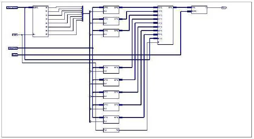
The proposed Multi-Functional Chip is implemented in VHDL and the code is synthesized using Xilinx ISE 8.1i. BKM-LM is loaded with different control words and various inputs were applied to check the functionality. The design is implemented for a XILINX SPARTAN 3E FPGA and target device selected was XC3S100E. Eight different standard functions shown in Table 1 are implemented on the proposed multi-functional chip. Control words of eight standard functions [19] are shown in Table 1 are loaded into BKM-LM. There are two modes of operation for this BKM-LM, program mode and functional mode. When PGM input is logic ‘1’ then BKM-Logic Module is in program mode and when PGM =logic ‘0’, then BKM-logic module is in function mode. In program
[image:9.595.140.458.362.502.2]mode the proposed logic module can be loaded with various control words to realize various functions. In function mode, the logic module realizes the function based on the value placed on FUN_ID bus. The RTL schematic of the proposed multi-functional chip is shown in Fig. 9. The proposed system offer several advantages over conventional logic modules. Conventional logic modules are not run time re-configurable, while the proposed BKM-LM is runtime reconfigurable and multi-functional. As the logic module behaves on the basis of control word given, application of a wrong control word results in a functionality which is different from the actual one. Table 2 shows the comparison of device utilization of the proposed system with some standard functions for SPARTAN 3E FPGA system.
Table 1 - Configuration Bits Of A BKM-LM
S.NO FUNCTIONALITY ID CON_BITS
1 AB’C 000 00100000
2 A’BC+A’B’C 001 00001010
3 A’BC+AB’C’ 010 00011000
4 A’B+BC’ 011 01001100
5 AB’+A’BC 100 00111000
6 A’BC+ ABC’+A’B’C’ 101 01001001
7 A’B+BC+AB’C’ 110 10011010
8 ABC’+A’B’C’+AB’C+A’BC 111 01101001
Table 2 – Comparison Of Device Utilization Details Of The Proposed Chip Implemented On Xilinx SPARTAN 3E
Function/Logic No. of Slices used No. of 4 input LUTS used
AB’C 1 1
A’BC+A’B’C 1 1
A’BC+AB’C’ 1 1
A’B+BC’ 1 1
AB’+A’BC 1 1
A’BC+ ABC’+A’B’C’ 1 1
A’B+BC+AB’C’ 1 1
ABC’+A’B’C’+AB’C+A’BC 1 1
BKM-LM as
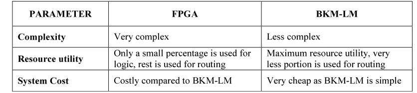
[image:9.595.120.475.551.716.2]Table 3 –Comparison Between FPGA And BKM-LM
PARAMETER FPGA BKM-LM
Complexity Very complex Less complex
Resource utility Only a small percentage is used for
logic, rest is used for routing
Maximum resource utility, very less portion is used for routing
System Cost Costly compared to BKM-LM Very cheap as BKM-LM is simple
7. CONCLUSION
This paper proposes a multi-functional chip which enhances security of digital systems with bit-stream encryption. Conventional FPGA based systems are not run time re-configurable. This new technique not only makes a system runtime reconfigurable, but also enhances the system security. Bit stream encryption is mainly employed to avoid copying of bit streams when they are loaded into the FPGAs. In the proposed system, as the design is partially or fully incomplete, the intruder should load the MFC with proper control word before proceeding further. By default, the MFC module is transparent, in the sense; it does not have any pre-defined functionality. The user, by loading the control words is injecting the intended functionality and so this system is more secure compared to other FPGA based systems. Compared to FPGA systems with less device utilization factor [18], all resources in the proposed system are utilized fully. Lot of power is utilized by the routing systems in the FPGA while proposed system is having a simple routing system which consumes very little power. Another advantage of the proposed system is its multi-functionality. This MFC can be used for the design of systems with digital rights management, i.e., same chip behaving is an entirely different way for different users. Also this new technique of Binary Key Multiplexing (BKM) can be useful in systems where different rights or permissions should be defined for different users. Table 3 shows a comparison between FPGA based systems and proposed BKM-LM.
The advantages of this new technique can be summarized as
• Provides security with less hardware overhead compared to systems with bit stream encryption.
• Reconfigurable at run time by loading the system with a new control word.
• Control words can be incorporated for the entire system or to certain blocks of the system based on the degree of security needed for the system.
REFERENCE:
[1] Binu K. Mathew, Dr. Zacharia K.P – New techniques to enhance FPGA based system security, International Journal of Advanced Research in Computer Engineering & Technology, Vol. 1, Issue 5, July 2012, pages 533 - 543.
[2] Binu K. Mathew, Dr. Zacharia K.P –New Logic Module for secured FPGA based system, International Journal of Electronics and Communication Engineering, Vol. 1, Issue 5, August 2012, pages 91-94.
[3] Saar Drimer, Volatile FPGA design security – a survey, Computer Lab, University of Cambridge,
[4] S. Drimer. Authentication of FPGA bit-streams: why and how. In Applied Reconfigurable Computing, volume 4419 of LNCS, pages 73– 84, March 2007.
[5] T. Huffmire, S. Prasad, T. Sherwood and R. Kastner, Threats and Challenges in reconfigurable hardware security.
[6] Ted Huffmire, S. Prasad, Tim Sherwood and Ryan Kastner, Designing Secure Systems on reconfigurable Hardware.
[7] Ted Huffmire, S. Prasad, Tim Sherwood and Ryan Kastner, Managing Security in FPGA-based embedded systems,
ISSN: 1992-8645 www.jatit.org E-ISSN: 1817-3195
[9] J. X Zheng, M. Potkonjak “Securing netlist level FPGA design through exploiting process variation and degradation”
[10] I. Kuon, R. Tessier and J. Rose, “FPGA Architecture: Survey and Challenges”, Foundations and Trends in Electronics Design Automation, Vol. 2, pages 135-253, 2007.
[11] W. H. Collins, “A Secure Reconfigurable System-On-Programmable Chip Computer system”, M.S. Thesis, Graduate School, University of Tennessee, 2013.
[12] L. Sekanina, R. Ruzicka, Z. Vasicek, V. Simek and P. Hanacek, “Implementing a unique chip ID on a Reconfigurable Polymorphic Circuit”, Information Technology and Control, Vol 42, No. 1, March 2013
[13] M. Abramovici and P. Bradley, “Integrated Circuit Security – New Threats and Solutions”, [14] A. C. Baumgarten, “Preventing integrated
circuit piracy using reconfigurable logic barriers”, M.S. Thesis, Graduate School of Computer Science, Iowa State University, 2009
[15] N. Valette, L. Torres, G. Sassatelli, and F. Bancel, “Securing embedded programmable gate arrays in secure circuits”, Proceedings 20th IEEE International Parallel & Distributed Processing Symposium, Greece, 2006
[16]R. Chaves, “Secure computing on reconfigurable systems”, PhD Thesis, Technical University of Lisbon, Lisbon, 2007
[17]K. M. Goertzel, and B. A. Hamilton, “Integrated circuit security threats and hardware assurance counter measures”, Crosstalk, November-December 2013
[18] A. DeHon, "Reconfigurable Architecture for general purpose computing”, report no AITR 1586, MIT AI Lab, 1996