ISSN: 1992-8645 www.jatit.org E-ISSN: 1817-3195
HIGH-LEVEL DESIGN FOR REAL TIME IMPLEMENTATION
OF CSC ALGORITHM ON FPGA USING MATLAB &
SIMULINK SIMULATION
MOHAMMED ALAREQI1,3, R.ELGOURI1,2 ,A.ZEMMOURI1, L.HLOU1
1
Laboratory of Electrical Engineering and Energy Systems, Faculty of Sciences, University Ibn Tofail Kenitra, Morocco
2
Laboratory of Electrical Engineering and Telecommunications Systems, National Schools of Applied Sciences, University Ibn Tofail Kenitra, Morocco
3
Community College, Sana'a, Yemen E-mail : [email protected]
ABSTRACT
This paper presents a methodology for very high-level image processing design and implementation real-time image processing applications on a re-configurable logic platform field programmable get array. This methodology aims to improve the design verification efficiency for such complex system. It presents a design and develops for two colors space converters (RGB to YCbCr and YCbCr to RGB), and application.
The proposed technique was implemented using Xilinx System Generator in MATLAB/SIMULINK environment on field programmable get array. To improve the implementation time, Xilinx system generator software for generating “hardware description language code” from a high-level MATLAB description has been used. A field-programmable gate array, Provide a major alternative in hardware platform scenario because of its reconfiguration character, marketing speed and low price and it provides us a custom hardware platform where we can design and develop the required algorithm and architecture by using different built-in a custom logic, Digital signal processingcores and automatic “hardware description language code” generation facility. A field-programmable gate array offer high performance in terms of processing speed and high chip density, thus suiting every conceivable application, whether small or high end, yet remaining cost-effective. The objective is to have a converter, which will be useful for number of applications due to the diversity of computers, Internet and a wide variety of video devices, all using different color representations, is forcing the digital designer today to convert between them. Performance of these design implemented in FPGA card XUPV5-LX110T.
Keywords: Color Space Converters (CSC), Field Programmable Get Array (FPGA), Xilinx System Generator (XSG).
1. INTRODUCTION
A color space is a method of describing and representing colors in a standard way. There are three popular groups of color spaces used to define colors in electronic devices, mainly RGB (used in display devices), YCbCr, YIQ and YUV (used in
video systems) and CMYK (used in color printing).Color space conversion (CSC) is the process of converting the representation of a given color or image from one color space to another [1].
All color spaces can be derived from the RGB information supplied by devices such as cameras and scanners. Different color spaces have historically evolved for different applications. In
each case, a color space was chosen for application-specific.
Color space conversion has become an integral part of image processing and transmission. Real time images and video are stored in RGB color space [2].Processing an image in the RGB color space, with a set of RGB values for each pixel is not the most efficient method. To speed up some processing steps many broadcast, video and imaging standards use luminance and color difference video signals, such as YCbCr, making a
mechanism for converting between formats necessary[3].
ISSN: 1992-8645 www.jatit.org E-ISSN: 1817-3195 in custom hardware because these functions operate
identically on each pixel .In software implementation the loop and the other overhead can be significant while in hardware Implementation only a small amount of circuitry is require. [4].FPGA’s are widely used to design applications that require high-speed parallel data processing, such as image processing [5]-[6]-[7]-[8].
Since an FPGA implements the logic required by an application by building separate hardware for each function, FPGAs are inherently parallel. This gives them the speed that results from a hardware design while retaining the reprogrammable flexibility of software at a relatively low cost. This makes FPGAs well suited to image processing, particularly at the low and intermediate levels where they are able to exploit the parallelism inherent in images [8].
The tools, which used to design and debug the different applications in FPGA, are Integrated Software Environment (ISE), Embedded Development Kit (EDK) and, System generator, which was used in this paper.
System generator is a tool provided by Xilinx and fully integrated into the MATLAB software. It is a block based graphical editor. A library of hardware blocks is available to the user. Instead of writing any hardware design by hand, the user can create its system by using prebuilt blocks. This tool decreases dramatically the development time and verification process of an application.
This reduces the time necessary between the control design derivations and hardware implementation. In addition, the software provides for the hardware simulation and hardware-in-the-loop verification, referred to as hardware co-simulation from within this environment [2]-[3]. This methodology provides easier hardware verification and implementation compared to HDL based approach. The Simulink simulation and hardware-in-the loop approach presents a far more cost efficient solution than other methodologies. The ability to quickly and directly realize a control system design as a real-time embedded system greatly facilitates the design process [9]-[10]-[11].
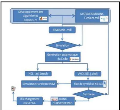
The tool (XSG) will program the targeted FPGA automatically and send the input data that need to be processed. When this is done, the results are displayed on the screen. Hence, the design can be tested in real-time on the targeted FPGA very quickly [12].The design flow of the XGS development tool is given in figure1.
The remainder of this paper is divided into five sections. After introduction, a description of color space is presented in section 2. Section 3 presents implementation, converting From RGB to YCbCr
Color Space, Converting from YCbCr to RGB
[image:2.612.316.518.203.387.2]Color Space and an example of image processing application on FPGA. Section 4shows some results and analysis. Finally, concluding remarks are given in Section 5.
Figure 1: Xilinx System Generator (X.S.G) design flow
2. COLOR SPACE
A color space is a method by which we can specify, create and visualize color. The purpose of a color modelis to facilitate the specification of colors in some standard, generally accepted way.
2.1 RGBColor Space
The Red, Green, and Blue color space is widely used in computer graphics. RGB is one of most widely used color space for processing and storing the digital image data[13].Red, Green, and Blue are the three primary colors and are represented by three-dimensional Cartesian coordinate system . It is an additive color space where each component has a range of 0 to 255, with all three 0s for producing a black color and all three 255 for producing a white color [14].Any other color space can be obtained by transformation from RGB.
ISSN: 1992-8645 www.jatit.org E-ISSN: 1817-3195 B). In RGB chrominance and luminance component
are mixed So RGB is not very efficient when dealing with real world images and thus processing an image in RGB color space is usually not the most efficient method [15].
2.2 YCbCr Color Space
YCbCr color space has been defined in response
to increasing demands for digital algorithms in handling video information and has become a widely used model in a digital video [16].
YCbCr one of two primary color spaces is
widely used to represent digital component video (the other is RGB). The difference between YCbCr
and RGB is that YCbCr represents color as
brightness and two color difference signals, while RGB represents color as red, green and blue. In YCbCr, the Y is the brightness (luma),Cb is blue
minus luma (B-Y) and Cr is red minus luma (R-Y).
YCbCr Color Space was developed as part of the
Recommendation ITU-R BT.601 for worldwide digital component video standard and then used in television transmissions (YCbCr) is used in the
context of digital image and video processing, especially, for JPEG images and MPEG video encoding) [15]-[3].
2.3 Converting From RGB to YCbCr Color
Space
Decomposing an RGB color image into one luminance image and two chrominance images is the method that has been used in the most commercial applications such as face detections, JPEG and MPEG imaging standards [17]-[15].
Engineers found 60% to 70% of luminance or brightness is in the "green color." In the chrominance part Cb and Cr, the brightness
information can be removed from the blue and red colors. To generate the same color in the RGB
format, all three-color components should be of equal bandwidth. This requires more storage space and bandwidth. Also, processing an image in the RGB space is more complex since any change in the color of any pixel requires all the three RGB values to be read, calculations performed, and then stored [4].
The conversion of RGB colors into full-range YCbCr colors is described by the following
equation: (1)
The other way round, to convert a full-range YCbCr color into RGB is described by the
following equation:
(2)
3. FPGA IMPLEMENTATION
3.1 RGB2YCbCr Top-Level Module
The above equation No (1) have been used to design the unit CSC (RGB to YCbCr) by using
ISSN: 1992-8645 www.jatit.org E-ISSN: 1817-3195
Figure 2: RGB 2 YCbCr top-level module
In Figure2, the three “Gateway In” blocks define the input interface of R, G, B and the three “Gateway Out” block define the output interface of Y, Cb and Cr for the RGB2YCbCr module. Every
System Generator diagram requires that at least one System Generator token be placed on the diagram. This token is not connected to anything but only serves to drive the FPGA implementation process. The property editor for this token allows you to specify the target Netlist, device, performance targets and system period.
RGB2YCbCr top-level module presented in
Figure2 is composed with calculate Y sub-module, calculate Cb module and calculate Cr
sub-module. The three sub-modules connection diagram isshown in Figure3, we can see that the R, G and B areinputted into the three sub-modulesandoutput the “Y”, the “Cb” and the “Cr”. The calculate y
sub-module receives the “R”, “G”and “B” to calculate Y; the seam withe calculate Cb sub-module to
calculate Cb and calculate Cr sub-module to
calculate Cr
Figure3: calculate Y, calculate Cb and calculate Cr
sub-module connection
3.1.1 Calculate Y sub-module
In this design the function of Y sub-module is to calculate the Y (luminance image) of the parallel input of the R, G and B value by the basic equations to convert between RGB and Y
Y = 0.299R + 0.587G + 0.114B (3)
Figure4: calculate Y sub-module in XSG
3.1.2 Calculate Cb Sub-Module
In this design the function of Cb sub-module is
to calculate the Cb (chrominance image) of the
parallel input of the R, G and B value by the basic equations to convert between RGB and Cb
Cb = –0.169R – 0.331G + 0.5B +128
(4)
Figure5: calculate Cb sub-module in XSG
3.1.3 Calculate Cr sub-module
In this design the function of Cr sub-module is
to calculate the Cr (chrominance image) of the
parallel input of the R, G and B value by the basic equations to convert between RGB and Cr
Cr = 0.5R – 0.419G – 0.081B +128
(5)
Figure6: calculate Cr sub-module in XSG
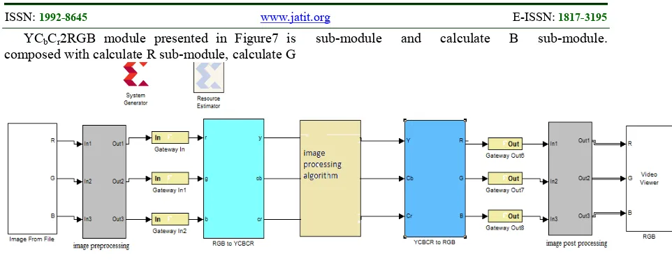
ISSN: 1992-8645 www.jatit.org E-ISSN: 1817-3195 YCbCr2RGB module presented in Figure7 is
composed with calculate R sub-module, calculate G
[image:5.612.87.568.72.259.2]sub-module and calculate B sub-module.
Figure 7:YCbCr2RGB with application top-level module
The three sub-modules connection diagram is shown in Figure8, we can see that the Y, Cb and Cr
are inputted into the three sub-modules and output the “R”, the “G” and the “B”. The calculate R sub-module receives the “Y” and “Cr” to calculate R;
the calculate “G” sub-module receives the “Y”, “Cb” and “Cr” to calculate Gand the calculate B
sub-module receives the “Y” and “Cb” to calculate
B
Figure8: calculate R, calculate G and calculate B sub-module connection
3.2.1 Calculate R sub-module
In this design, the function of R sub-module is to calculate the Rof the parallel input of the Y and Cr value by the basic equations to convert between
YCbCr and R
R = Y + 1.4(Cr-128)
(6)
Figure9: calculate R sub-module in XSG
3.2.2 Calculate G sub-module
In this design, the function of G sub-module is to calculate the Gof the parallel input of the Y, Cb
and Cr value by the basic equations to convert between YCbCr and G
G= Y -0.343(Cb-128) -0.711(Cr-128)
(7)
Figure10: calculate G sub-module in XSG
3.2.3 Calculate B sub-module
ISSN: 1992-8645 www.jatit.org E-ISSN: 1817-3195 Cb value by the basic equations to convert between
YCbCr and B
B = Y +1.765(Cb-128) (8)
Figure11: calculate B sub-module in XSG
3.2.4 Image processing algorithm (edge detection)
YCbCr2RGB module presented in Figure7
shown Image processing algorithm subsystem.The application that we used in this subsystem is edge detection. The Image edge detection is very powerful and used method in the field of Image processing applications. Edge detection plays an essential role to detect edges of an object. In Different fields like medical application, for object detection in aerial images from satellite and vehicle detection etc. A set of mathematical methods for identifying points in a digital image at which the image brightness changes sharply or has discontinuities is named as edges.
In this paper, the edge detection algorithm represented by the Transfer function as Shown in Figure12.
Figure12: edge detection algorithm
3.3 Hardware Co-Simulation
System Generator provides hardware co-simulation, making it possible to incorporate a
design running in an FPGA directly into a Simulink simulation "Hardware Co-Simulation". Using hardware co-simulation, we can select a subsystem in a System Generator model to run in hardware while the rest of the model is simulated on a host PC.Hardware co-simulation block was generated without any errors and the processing speed and hardware resources were obtained using the synthesis Moreover, ISE implementation tool.
Further, while the simulation is carried outby connecting the hardware run-time model, that is, Virtex 5 platform (Virtex5 XUPV5-LX110T), to design and perform the simulation, it iscalled as HIL verification. Figure 13 shows the view of the HDL co-simulation and HIL circuit.
JTAG and Ethernet point-to-point communication are the two most widely used hardware co-simulation interfaces.
System Generator provides a generic interface that uses JTAG and a Xilinx programming cable (e.g., Parallel Cable IV or Platform Cable USB) to communicate with FPGA hardware.
Figure13: HDL co-simulation and HIL circuit
4. RESULT AND ANALYSIS
Color space converters R’G’B’ ↔ Y’CbCr
algorithm, and edge detection, are designed in MATLAB and Simulink (system generator) and they are implemented on Virtex-5. The RGB2YCbCr module in Figure2 is behaviorally
ISSN: 1992-8645 www.jatit.org E-ISSN: 1817-3195 Table1 and table2, details the resource
requirements of the CSC design. Note that in practice, additional blocks are needed for input/output interfaces and synchronization
Table 1: Post Synthesis Device Utilization
Ofrgb2ycbcr Top-Level Module
Table 2: Post Synthesis Device Utilization
Ofycbcr2rgb Top-Level Module
The Top-level RTL schematic for the CSC (RGB 2 YCbCr) and CSC (YCbCr 2 RGB)
developed and implemented on FPGA is shown in figure14and figure15 respectively. This is a schematic representation of the preoptimized design shown at the Register Transfer Level (RTL). This representation is in terms of generic symbols, such as adders, multipliers, counters, AND gates, OR gates and is generated after the HDL synthesis phase of the synthesis process. The two default clock drivers are available for the system. This system blocks are designed for the Virtex-5 ML505 board.
Figure14: RTL Schematic For RGB2YCbCr Top-Level
Module
Figure15: RTL Schematic Forycbcr2rgb Top-Level Module
The algorithms and architectures are tested with three different images. The results are shown in
ISSN: 1992-8645 www.jatit.org E-ISSN: 1817-3195 RGB2YCbCr Top-Level
Module
RGB2YCbCr Top-Level
Module
YCbCr2RGB Top-Level Module
with (edge detection)
Input images
RGB 512*512 RGB 384*512 RGB 300*300
Output images
YCbCr YCbCr RGB
Output images
Y Y R
Output images
Cb Cb G
Output images
Cr Cr B
Figure11: Results of R’G’B’ ↔ Y’CbCr top-level module
5. CONCLUSION
Processing an image in the RGB color space, with a set of RGB values for each pixel is not the most effective method. To accelerate certain processing steps many broadcast, video and imaging standards use luminance and color difference video signals, such as YCbCr, making a
mechanism for converting between formats necessary. (RGB ↔ YCbCr) conversions require
enormous computing power.
The use of the Xilinx System Generator tool for colors space converters is presented. It is shown that this tool is ideal for developing FPGA based
hardware without the requirement of learning HDLs and Hardware Design.
The results indicate the Xilinx System Generator tool offers an easy and efficient method for implementing colors space converters (RGB ↔ YCbCr) algorithm into FPGA. The design was
implemented on virtex5 devices and their utilization summaries are showed.
ISSN: 1992-8645 www.jatit.org E-ISSN: 1817-3195 techniques used for processing images with
minimum resources and minimum delay. There is possibility of implementing some more parallel, processes with the architecture of CSC on the same FPGA because; we used 138 CLB slices with 1% utilization.
The future work will be focused on Xilinx System Generator development tools for the implementation of other blocks used in computer vision on Xilinx Programmable Gate Arrays (FPGA).
REFERENCES
[1] S. Patil, “Reconfigurable Hardware for Color Space Conversion”,Thesis Submitted in Partial Fulfillment of the Requirements for the Degree of Master of Science in Electrical
Engineering,Rochester Institute of Technology
Rochester, New York,2008.
[2] K. Jack, “Video Demystified A Handbook for the Digital Engineer”, LLH Technology
Publishing, Fifth Edition, 2007.
[3] Y. Said, T. Saidani and M. Atri, “High-Level Design for Image Processing on FPGA Using Xilinx AccelDSP”,Proceedings IEEE
International Conference onComputer
Applications and Information Systems
(WCCAIS),2014, pp.1-5.
[4] B. Ahirwal, M. Khadtare and R. Mehta, “FPGA based system for Color Space Transformation RGB to YIQ and YCbCr”,IEEE International Conference on
Intelligent and Advanced Systems, 2007,
PP.1345-1349.
[5] R.Harinarayan, R. Pannerselvam, M. Mubarak Ali, and D. Kumar Tripathi, “Feature extraction of Digital Aerial Images by FPGA based implementation of edge detection algorithms” ,IEEE International Conference on Emerging Trends in Electrical and
Computer Technology (ICETECT), March
2011,pp.631 – 635.
[6] C.JohnMoses, D.Selvathi, and S.SajithaRani, “FPGA Implementation of an Efficient Partial Volume Interpolation for Medical Image Registration”,IEEE International Conference on Communication Control and Computing
Technologies (ICCCCT-10),
Oct.2010,pp.132–137.
[7] Z. Shanshan and W.Xiaohong, “Vehicle Image Edge Detection Algorithm Hardware Implementation On FPGA”,International
Conference on computer Application and
System Modeling(ICCASM ), Taiyuan,
vol.11,oct.2010,pp184-188.
[8] M.Alareqi, K.Mateur, R.Elgouri and L.Hlou,“FPGA Based Image Processing Algorithms (Digital Image Enhancement Techniques) Using Xilinx System Generator”
European Journal of Scientific Research,Vol.
134 No 3 , 2015, pp.336-346.
[9] Donald Graeme Bailey, “Design for embedded image processing on FPGAs”, book, 2011.
[10] Xilinx System Generator User's Guide, www. Xilinx.com
[11] Inc., T.M: Embedded Matlab Language User Guide, The MathWorksInc, 2007.
[12] T. Saidani, D. Dia, W. Elhamzi, M. Atri and R. Tourki,“Hardware Co-simulation For Video Processing Using Xilinx System Generator”,Proceedings of the World
Congress on Engineering ( WCE),London
U.K, vol.1,2009,pp.1-5.
[13] D. Christophe, “Multicore processing engines for machine vision, image analysis and data compression”, theses of Ph.D. from Illinois institute of technology, 2010.
[14] J. Yang, W. Lu and A. Waibel,“Skin-color modeling and adaptation”,Third Asian Conference on Computer Vision Hong Kong
China, vol.2, 1998, pp.687-694.
[15] T.S. Wong, C. A. Bouman, Fellow, IEEE, I. Pollak, and Z. Fan, "A Document Image Model and Estimation Algorithm for Optimized JPEG Decompression", IEEE
Transactions on Image Processing, Vol. 18,
Nov. 2009, pp. 2518 – 2535.
[16] A. F. Mahmood and A. M. Salih, “Implementation of Multiplier less Architectures for Color Space Conversions on FPGA”,Al-Rafidain Engineering, vol. 19, 2010, pp. 89-103.
[17] A. Kaur and B.V Kranthi, “Comparison between YCbCr Color Space and CIELab
Color Space for Skin Color
Segmentation”,International Journal of
Applied Information
Systems,vol.3,2012,pp.30-33.
[18] N. Tiwari and S.C.Reddy,"Performance Measurement of a Fully Pipelined JPEG Codec on Emulation Platform", Advance
Computing Conference (IACC) IEEE 2nd