PARALLEL INTERFACE ADAPTOR 2200-420 . JUNE 10, 1972
DATAPOINT CORPORATION
PRODUCT SPECIFICATION
6/10/72.
PARALLEL INTERFACE ADAPTOR
1.0 General Description 2.0 System Requirements 3.0 Technical Description
3.1 Device Address Control 3.2 Data Input Buffer/Register 3.3 Status Input Buffer/Register 3.4 Data Output Register/Buffer 3.5 Command Register/Buffer 3.6 Control Strobe Buffer 3.7 Power On Reset
4.0 Physical Description
5.0 Environmental Requirements 6.0 Interface Requirements 7.0 Options
2200-420
7.1 Data Inputs (from external device) 7.2 Status Input (from external device) 7.3 All Outputs
7.4 Data Outputs 7.S Command Outputs 7.6 Control Strobes 7.7 System Reset Strobe
7.8 Interface Address Status 7.9 Address
8.0 Parts Lis t~
1.0 GENERAL DESCRIPTION
The DATAPOINT 2200-420 Parallel Interface Adaptor is designed
to interface the DATAPOINT 2200 to any peripheral equipment that
requires parallel data. The DATAPOINT 2200 interchanges data with
all peripherals over the same 8 bit data input/output bus,
re-quiring that devices placed on this bus follow stringent rules as
to when and what data is placed on it. The Parallel Interface
Adaptor provides for addressing, status and data modes, and data
buffering, so that the external device only has to present its
outputs and receive its inputs from the Parallel Interface Adaptor.
2.0 SYSTEM REQUIREMENTS
The 2200-420 requires only two cables for operation. One is
a standard I/O cable (supplied with 2200-420) between the
2200-420 and the DATAPOINT 2200. Through this cable the 2200-420
receives all operating power and makes the necessary connections
to the DATAPOINT 2200 I/O bus. The second cable connects the
2200-420 to the external device to be interfaced. This cable will
vary, depending on the characteristics of the external device.
Power for the 2200-420 is derived from the DATAPOINT 2200
for one or two adaptors. Additional adaptors require supplemental
power.
3.0 TECHNICAL DESCRIPTION
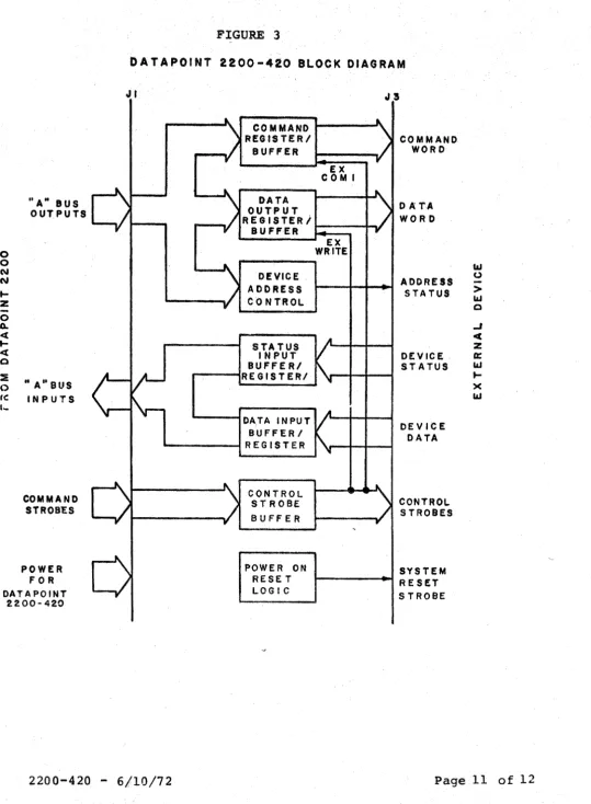
The 2200-420 has seven major sections:
1. DEVICE ADDRESS CONTROL
2. DATA INPUT BUFFER/REGISTER
3. STATUS INPUT BUFFER/REGISTER
4.-1lIIi.IA OUTPUT REGISTER/BUFFER
5. COMMAND REGISTER/BUFFER 6. CONTROL STROBE BUFFER
7. POWER
ON
RESET3.1 Device Address Control
Each 2200-420 connected to the DATAPOINT 2200 I/O bus -must
have a unique address so that it can determine if the data is
meant for (it. If the 2200-420 is not currently addressed, all
data or status transfer to the DATAPOINT 2200 I/O bus is inhibited.
Likewise, the control strobes are inhibited from being sent to the
external device. When the 2200-420 is addressed, i t will present a
"I" on the interface address status output. For the remainder
of this t~chnical description, i t will be assumed that the
2200-420 is addressed.
The 2200-420 is factory wired for an I/O address of 2268" This
may be field changed to any other address at any time.
When the 2200-420 is addressed, i t will present either the
DATA or STATUS of the external device to the DATAPOINT 2200. This
is determined by the DATA MODE or STATUS MODE operation of the
2200-420.
The 2200-420 is placed in the STATUS MODE whenever an EX
ADDRESS strobe is received from the DATAPOINT 2200. It can also be
placed in the STATUS MODE without re-addressing by receiving an
EX STATUS strobe. When in the STATUS MODE the 2200-420 will present
\
to the DATAPOINT 2200 the information contained in the STATUS
INPUT REGISTER.
The 2200~420 can be placed in the DATA MODE by an EX DATA
strobe from the DATAPOINT 2200. When in the DATA MODE, the
2200-420 will present to the DATAPOINT 2200 the information
con-tained in the DATA INPUT REGISTER.
If the 2200-420 is not addressed, it will not respond to
any commands from the DATAPOINT 2200 nor will it return any data
or status to the DATAPOINT 2200.
3.2 Data Input Buffer/Register
The eight data inputs to the 2200-420 from the external
device are received by high-impedance differential comparators.
The input impedance is about 15K ohms and the inputs are
over-voltage protected and integrated for noise rejection. The
decision level is +2.4 volts to.3 volts. The DATA INPUT REGISTER
can be latching or non-latching. If the latching mode is chosen,
the DATA INPUT REGISTER will hold the data present at the data
input terminals when input status bit S7 is strobed.
3.3 Status Input Buffer/Register
The STATUS INPUT BUFFER/REGISTER is ari a-bit register
in-tended to hold status information from the external device (xmit
ready, receive ready, etc.). The STATUS INPUT REGISTER can be
made latching or non-latching. If the latching mode is chosen,
status bits 0 - 6 will be reset upon the execution of any INPUT
instruction by the DATAPOINT 2200 while the 2200-420 is in the
STATUS MODE (see STATUS/DATA -Section 3.1). Status bit 7 can be
reset at the same time as bits 0 - 6 or optionally by the
execution of an INPUT instruction while in the DATA MODE. The
inputs of the STATUS INPUT BUFFER have the same electrical
characteristics as the DATA INPUT BUFFERS (Section 3.2).
3.4 Data Output Register/Buffer
The DATA OUTPUT REGISTER/BUFFER is an a-bit register to hold
data from the DATAPOINT 2200 to the external device. This register
is set to the contents of the I/O bus at the execution of an EX
WRITE instruction l::>Y the DATAPOINT 2200 • The contents of the DATA OUTPUT REGISTER/BUFFER will not change until the execution of the
next EX WRITE instruction by the DATAPOINT 2200.
The DATA OUTPUT BUFFER is an open collector TTL gate, making
the outputs .TTL compatible. At the ground state i t will sink
approximately 35 rna and in the high state it will source about 1
rna. A low output is between 0 and +. 4 volts; a high output is +5 or +12, depending on the option selected.
3.5 Command Register/Buffer
The COMMAND REGISTER is an 8-bit register typically used to
send a command word to the external device. This register is set
to the contents of the DATAPOINT 2200 I/O bus when an EX COMl
instruction is executed by the DATAPOINT 2200. The, COMMAND
REGISTER will not change until another EX COMl is executed.
The electrical characteristics of the COMMAND BUFFER are
the sarne as the DATA OUTPUT BUFFER (Section 3.4).
3.6 Control Strobe Buffer
The following control strobes are gated to occur only while
the 2200-420 is addressed. They are buffered to provide the same
electrical characteristics as the DATA OUTPUT BUFFER (Section 3.4).
SENSE SENSE WRITE COM]" COM2 COM 3 COM4
STATUS - also puts PARALLEL INTERFACE in STATUS MODE
DATA - also puts PARALLEL INTERFACE in DATA MODE
- also loads DATA OUTPUT REGISTER - also loads COMMAND REGISTER
3.7 Power On Reset
When system power is applied (by turning on the DATAPOINT
2200) the DATA OUTPUT REGISTER and COMMAND REGISTER are set to
"0 ,. and a one millisecond pulse occurs on the system reset strobe •
This pulse may be used to initiate the 'external device at power
on.
4.0 PHYSICAL DESCRIPTION
See Figure 1 for outline drawing.
S.O ENVIRONMENTAL REQUIREMENTS
0° to SooC (32° to 122°F)
10 to 9S% relative humidity
6.0 INTERFACE REQUIREMENTS
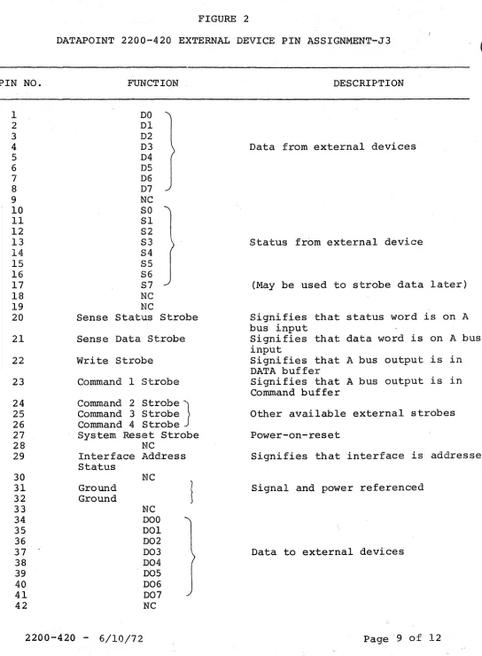
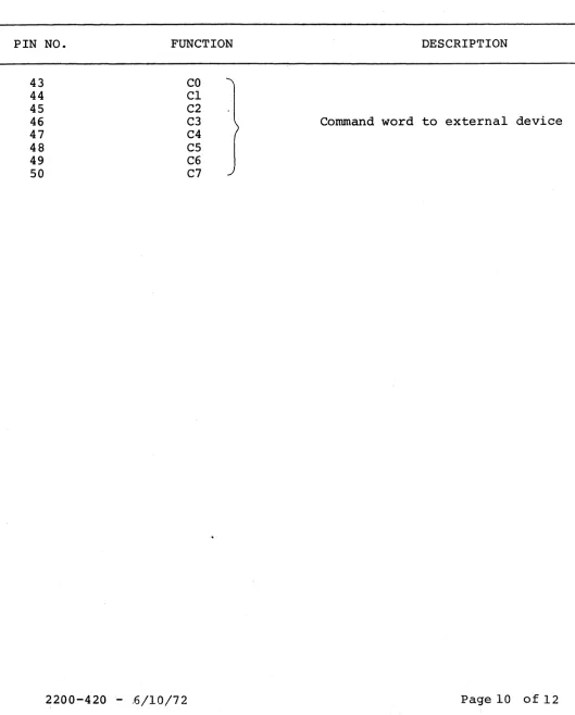
See Figure 2 for pin connections and signal names.
7.0 OPTIONS
The following options are fully strappable and changes in
configuration may be made by a technician in the field as
de-sired. Factory preparation straps those options noted as standard.
prior to shipment.
7.1 Data Inputs (from external device)
a) latching (on S7) (E23-E24 jumpered)
b) non-latching (pass-thru mode) (standard) (E23,E24 open)
c) ground true (standard) (El-E2[E3 open])
d) high true (E3-E2 [Elopen])
7.2 Status Input (from external device)
a) latching (standard) (E7-E8/E9-E10/Ell-E12/E13-E14/E1S-E16/
E17-E18/E19-E20 pairs jumpered)
b) reset S7 in data mode (standard) (ES6-ES7 [ESS open])
c) reset S7 in status mode (E56-ESS [ES7 open])
d) non-latching (jumpers in "a" above open)
e) ground true (standard) (E4~ES [E6 open])
f) high true (ES-E6 [E4 open])
I 7.3 All Outputs
a) high = +5 volts (standard) (E35-E34 [E36 open])
b) high
=
+12 volts (E35-E36 [E34 open])7.4 Data Outputs
a) ground true (standard) (E4l-E40 [E42 open)
b) high true (E42-E4l [E40 open])
7.5 Command Outputs
a) ground true (standard) (E37-E38 [E39 open])
b) high true (E38-#39 [E37 open])
7.6 Control Strobes
a) ground true (standard) (E25-E26 [E27 open])
b) high true (E26-E27 [E25 open]) ,
7.7 System Reset Strobe
a) high for reset (E29-E30 [E28 open])
b) low for reset (standard) (E28-E29 [E30 open])
7.8 Interface Address Status
a) high for addressed (E33-E32 [E3l open])
b) low for addressed (standard) (E3l-E32 [E33 open])
7.9 Address
a) any address optional (see below)
b) standard address is 226
ADDRESS BYTE
--~----~--~---(2 2 6'
~(O ~
0 '\( 1~
0 ')I
E~41
E:7/E~ol
Ei,3[E!5IE~81 E~1IE~41
I I I I
E43 E49 E46 E52
-'-Octal
Binary
"A" Bus Output Terminal Numbers
Gate Input Terminals
Jumper gate inputs to address byte zero bit terminals.
IV IV o o I .c:. IV o I-d ru l.Q (1) 00 0 Hl ... IV
10.5
..
2. 7"
t
TOP VIEW
L.-r - - - : -
15.511---~~1
r
-
-
- -
-
- -
-
-
"1I
II
(II
I
Ifft?
(
I
I
(
,-- -t,
I
II
~---, ,;.I · -++
"--1'
I
I' l
-++- I
I
't--I I
I I
I
JI
I
.:'
II
I
II
r-
..A1J:~
.r
(
-L -r
-1
r- 10.0"
--
• ICOVER
BASE PLATE
" I .... P t.. 6 . . . . 11.'
•
6.0 II
t
REAR VIEW
"---~I
10.2
I
/0 0( .12
10
o(
'--~--FIGURE 1
FIGURE 2
DATAPOINT 2200-420 EXTERNAL DEVICE PIN ASS:tGNMENT~J3
PIN NO.
1 2 3 4 5 6 7 8 9
~ 10
11 12 13 14 15 16 17 18 19 20 21 22 23 24 25 26 27 28 29 30 31 32 33 34 35 36 37 38 39 40 41 42 FUNCTION DO 01 02 03 04 05 06 07 NC SO Sl S2 S3 S4 S5 S6 S7 NC NC
Sense Status Strobe
Sense Data Strobe
Write Strobe
Command 1 Strobe
Command 2 StrObe}
Command 3 Strobe
Command 4 Strobe
System Reset Strobe NC
Interface Address Status Ground Ground NC NC 000 001 002 003 004
.. DOS
006 007
NC
2200-42.0 - 6/10/72
DESCRIPTION
Data from external devices
Status from external device
(May be used to strobe data later)
Signifies that status word is on A bus input
Signifies that data word is on A bus input
Signifies that A bus output is in DATA buffer
Signifies that A bus output is in
Command buffer
Other available external strobes
Power-on-reset
Signifies that interface is addressed
Signal and power referenced
Data to external devices
u
PIN NO.
43
44
45
46
47
48 49 50
FIGURE 2
DATAPOINT 2200-420 EXTERNAL DEVICE PIN ASSIGNMENT-J3 (Continued)
FUNCTION
CO Cl
C2
C3
C4 C5 C6 C7
DESCRIPTION
Command word to external device
[image:11.612.48.577.103.761.2]o
o
N
'"
...
Z
-o Go <[...
<[ o :i o rc I .... A" BUS OUTPUTS MA"eus INPUTS COMMAND STROBES POWER FOR DATA POINT 2200-420
FIGURE 3
DATAPOfNt 2200-420 BLOCK DIAGRAM
"I
COMMAND. REGISTERI BUFFER DEVICE. ADDRESS CO NTROL STATUS INPUT BUFFERI ... - - - I R E GIS T E R IDAtTA INPUT BUFFERI
" - - - . . l RE GIS T E R
CONTROL S T ROBE
BUFFER
POWER ON RESE T LOGIC EX COMI EX WRITE COMMAND WORD .DATA WORD ADDRESS STATUS DEVICE, STATUS DEVltE DATA CONTROL STROBES
1---"';-'-+01 S Y S T E M RESET STROBE
'"
(.) ->'"
o ..I C Z 0:: LtJ...
)('"
[image:12.617.22.562.15.750.2]8.0 PARTS LIST
The following separate parts are part of the 2200-420 and
are included in each shipment:
Quantitl DescriEtion
1 2200-420 Parallel Interface Adaptor
1 2200-160 Universal I/O Cable
1 2200-436 Connector Kit
1 Reference Manual
1 Test Tape Cassette
1 Test Connector