Thesis by
Qing He
In Partial Fulfillment of the Requirements for the Degree of
Doctor of Philosophy
California Institute of Technology
Pasadena, California
2006
© 2006
Qing He
First and foremost, I would like to thank my advisor, Professor Yu-Chong Tai, for
giving me the opportunity to work under his guidance on the fascinating field of MEMS.
His admirable expertise, endless supply of ideas, and passion for work made my Ph.D.
study fruitful and enjoyable. I will not forget the talks beyond academia that we had,
especially those during long carpooling hours. He certainly has taught me not only how to
succeed in academia, but also how to succeed in life.
My experience would not have been as meaningful without the other members of
the group. My gratitude goes to the previous group members who helped me to start this
journey, including Dr. Xing Yang, Dr. Tze-Jung Yao, Dr. Yong Xu, Dr. Ellis Meng, and Dr.
Jun Xie. I am grateful to Xing, not only for helping me academically, but also for being a
great friend in life. He gives help whenever needed and always provides invaluable advice.
I still remember clearly how Yao taught me to draw my first mask and gave me tips on how
to survive the Ph.D. program. Ellis is very nice and interesting to talk to and gives me lots
of help. Yong and Jun always made themselves available to help me with my design and
process issues, which enabled me to succeed faster. I am very fortunate to have Yong, Jun,
and their wives to be among my best friends, who greatly enriched my life at Caltech.
Thanks to all my colleagues in the group: Matthieu Liger, Justin Boland, Ted
Harder, Victor Chi-Yuan Shih, Scott Miserendino, Changlin Pang, Angela Tooker, Siyang
Zheng, Po-Jui Chen, Quoc Quach, Wen Li, Nick Lo, Damien Rodger, Jason Shih, Tanya
significant and also appreciated.
The interdisciplinary nature of my work has allowed me to have many great
collaborators. I would like to thank Prof. Terry D. Lee, Dr. Yunan Miao, and Dr. Jun Liu at
City of Hope. They have provided much guidance and assistance for my research. The
same gratitude goes to Prof. Jerry Pine, and his students Christopher Rutherglen and Jon
Erickson for their assistance on my first neuro-cage project. I want to acknowledge Prof.
Ray Deshaies, Dr. Siddharth Dasgupta, and Johannes Graumann for their help in the
tandem-LC project. It has been a great pleasure to interact with and learn from these great
people from different disciplines.
I am deeply grateful to my parents and my wife’s parents who are always there for
us. Especially, I want to thank my mother for her unconditional love. She cared so deeply
for my education at every stage of my life, for which I am deeply appreciative. My
mother-in-law helped tremendously when my first baby was born, which gave me plenty of
time for research. The time she stayed with us was one of the merriest during my Ph.D.
study.
Finally, my deepest gratitude is to my wife, whose love, support, and company has
been one of the greatest sources of strength for me. She has the magic to make my longest
days feel like the blink of an eye, while turning my bits and pieces of free time into
fascinating lifetime memories. We have two incredible daughters who deserve attention,
Katherine and Vivien, their smiles and laughter always keep me optimistic, energized, and
Integrated Nano Liquid Chromatography
System On-a-Chip
Thesis by Qing He
Doctor of Philosophy in Electrical Engineering California Institute of Technology
Integrated liquid chromatography (LC) chips are valued because of their significant
advantages over conventional systems. However, they are very challenging to build due to
the high complexity of LC systems and the need for high-level integration of many discrete
microfluidic devices.
The goal of this thesis is to develop technologies and devices towards a totally
integrated LC system on-a-chip. Using parylene microfluidics technology, all of the
devices are integrated on silicon wafers with CMOS-compatible batch processes. Due to
the small size of the on-chip LC columns, the chips all perform nano LC, which means that
the flow rates are on the scale of nano liters per minute.
integrate beads into micromachined devices. The technology is applied to make an
LC-ESI (Electro-Spray Ionization) chip with an integrated bead column packed with 5
µm diameter C18 silica beads. The integrated ESI nozzle allows direct coupling to a mass
spectrometer (MS).
Due to the high-pressure nature of LC operations, a complete LC chip must be
able to both withstand and generate high pressures on-chip. Therefore, an anchoring
technique is developed to dramatically increase the pressure rating of parylene devices
from about 30 psi to 1000 psi. In addition, on-chip high-pressure generation is achieved
with electrolysis-based micro-actuators.
An integrated ion liquid chromatography chip is demonstrated, which has on-chip
column, filters, injection structure, and conductivity detector. The column is packed with
7 µm anion-exchange beads with a slurry packing technique. On-chip sample injection,
separation, and detection of seven common anions are successfully demonstrated with a
sensitivity of 1 ppm.
Finally, a microchip that demonstrates high-pressure LC with integrated ESI
coupling to MS is presented. The capacity of the column, which is 6.5 cm long and
packed with 5 µm C18 silica beads, is the highest of all the devices in the thesis. Gradient
separation at a pressure of 450 psi and on-line MS detection of digested cytochrome c
Table of Contents
Chapter 1 Introduction
... 11.1 From IC to MEMS... 1
1.2 Micro-Electro-Mechanical Systems ... 3
1.2.1 Introduction... 3
1.2.2 Advantages ... 4
1.2.3 Fabrication Technologies... 6
1.2.4 From MEMS to µTAS ... 7
1.3 Microfluidics, Lab-on-a-Chip, and µTAS ... 7
1.3.1 Introduction... 7
1.3.2 Future Challenges ... 9
1.4 Parylene Microfluidics Technology... 11
1.4.1 Introduction to Parylene ... 11
1.4.2 Parylene Technology for Liquid Chromatography On-a-Chip ... 15
1.5 Bibliography ... 17
Chapter 2 Nano HPLC
... 212.1 High-Performance Liquid Chromatography... 21
2.1.1 Introduction... 21
2.1.2 History ... 23
2.1.3 Theory... 25
2.1.3.1 Chromatogram and Important Equations ... 25
2.1.3.2 Band Broadening and van Deemter Equation... 29
2.1.3.3 Band Broadening vs. Separation... 31
2.1.4.1 Solvents... 35
2.1.4.2 Pumps... 35
2.1.4.3 Sample Injectors... 35
2.1.4.4 Chromatographic Columns ... 36
2.1.4.4.1 Column Dimension... 36
2.1.4.4.2 Column Packing Physical Properties... 37
2.1.4.4.3 Base Material and Bonded Phases... 38
2.1.4.4.4 Separation Mechanisms... 41
2.1.4.5 Detectors ... 42
2.2 Nano HPLC ... 46
2.2.1 Definition... 46
2.2.2 Miniaturization Benefits ... 47
2.3 Review of Nano HPLC Chips... 50
2.4 Bibliography ... 54
Chapter 3 Bead Integration Technology and an LC-ESI/MS Chip
... 573.1 Introduction... 57
3.2 Working with Beads... 58
3.2.1 Various Terms and Properties ... 58
3.2.2 Aggregation ... 59
3.2.3 Packing and Porosity ... 60
3.2.4 Applications in MEMS ... 62
3.3 Integrating Beads into Micromachined Device ... 63
3.3.1 The Method... 63
3.3.2 Mixing and Spin-Coating ... 66
3.3.5 Releasing... 71
3.4 LC-ESI/MS Chip with Integrated Bead Column... 73
3.4.1 Introduction... 73
3.4.2 Design ... 73
3.4.3 Microchip Fabrication and Packaging ... 74
3.4.3.1 Fabrication Process ... 74
3.4.3.2 Photoresist Releasing Issue... 77
3.4.3.3 Packaging ... 81
3.4.4 Testing Results and Discussion ... 82
3.4.4.1 Bead Releasing and Column Packing ... 82
3.4.4.2 Pressure Rating ... 86
3.4.4.3 Electrospray to a Mass Spectrometer... 87
3.4.4.4 Method Validation... 89
3.5 Summary... 90
3.6 Bibliography ... 92
Chapter 4 High-Pressure Parylene Microfluidics... 95
4.1 Introduction... 95
4.2 High-Pressure Rating through Anchoring ... 96
4.2.1 Background... 96
4.2.2 Design ... 97
4.2.3 Fabrication ... 97
4.2.4 High-Pressure Packaging... 99
4.2.5 Pressure Rating Testing Results and Discussion ... 103
4.3 High-Pressure Generation through Electrolysis ... 106
4.3.2.1 Design and Fabrication ... 108
4.3.2.2 Electrolysis Bubble Generation and Recombination ... 110
4.3.3. An Electrolysis Device for High-Pressure Generation... 113
4.3.3.1 Design and Fabrication ... 113
4.3.3.2 Testing Method and Results ... 115
4.4 Summary... 117
4.5 Bibliography ... 118
Chapter 5 Ion Chromatography On-a-Chip... 119
5.1 Introduction... 119
5.1.1 Abstract... 119
5.1.2 Ion Chromatography... 120
5.1.3 Nitrate Sensing... 123
5.2 Microchip Design ... 124
5.2.1 Chip Design and Operation ... 124
5.2.2 Conductivity Sensing... 128
5.2.2.1 Conductivity Response Theory ... 128
5.2.2.2 Conductivity Detector Cell Analysis... 132
5.2.2.3 The On-Chip Conductivity Detector... 134
5.2.3 Downscaling ... 135
5.3 Microchip Fabrication ... 138
5.3.1 Fabrication Process Flow... 138
5.3.2 Chip Packaging... 142
5.4 Testing Results and Discussion ... 143
5.4.1 Separation Column Packing ... 143
5.4.4 Ion Chromatography Separation... 149
5.5 Summary... 151
5.6 Bibliography ... 153
Chapter 6 A Nano HPLC/MS Chip
... 1576.1 Introduction... 157
6.2 Design and Fabrication ... 158
6.2.1 Microchip Design ... 158
6.2.2 Fabrication Process... 159
6.2.3 Processing Challenges ... 164
6.2.3.1 Bubbling... 164
6.2.3.2 Black Silicon ... 168
6.2.4 Packaging... 169
6.3 Testing Results and Discussion ... 170
6.3.1 Column Pressure Rating ... 170
6.3.2 Pressure–Flow Rate Relation... 170
6.3.3 LC Separation with On-Line MS Detection ... 172
6.4 Summary... 173
6.5 Bibliography ... 175
List of Figures
Figure 1-1 (a) The first transistor (Bell Labs); (b) The first integrated circuit (Texas
Instruments); (c) Moore’s law (Intel); (d) State-of-the-art CPU chip Pentium 4 (Intel)... 2
Figure 1-2 Dimensions of MEMS, nanotechnology, and lab-on-a-chip... 3
Figure 1-3 Famous MEMS devices ... 5
Figure 1-4 Illustration of bulk micromachining and surface micromachining ... 7
Figure 1-5 Chemical structures of parylene N, C, and D... 11
Figure 1-6 Parylene deposition system and the involved chemical processes... 14
Figure 1-7 Parylene microfluidic devices ... 16
Figure 2-1 Illustration of the chromatographic separation process ... 22
Figure 2-2 The inventor of chromatography, Tswett, and his chromatographic device ... 23
Figure 2-3 Chromatogram and its characteristic features ... 25
Figure 2-4 Illustration of band broadening during chromatographic elution ... 29
Figure 2-5 Four mechanisms of band broadening ... 30
Figure 2-6 Van Deemter Curve ... 31
Figure 2-7 Band broadening effect vs. separation effect ... 32
Figure 2-8 Definition of HETP ... 34
Figure 2-9 Schematics for a typical HPLC system... 34
Figure 2-10 Injection valve working mechanism ... 36
Figure 2-11 Physical properties of liquid chromatographic beads ... 37
Figure 2-12 Chemical modification of silica surface... 39
Figure 2-13 Chemical structure and 3D illustration of C18 functional groups on silica surface ... 40
... 49
Figure 3-1 Two common particle packing structures (a) BCC; (b) FCC... 61
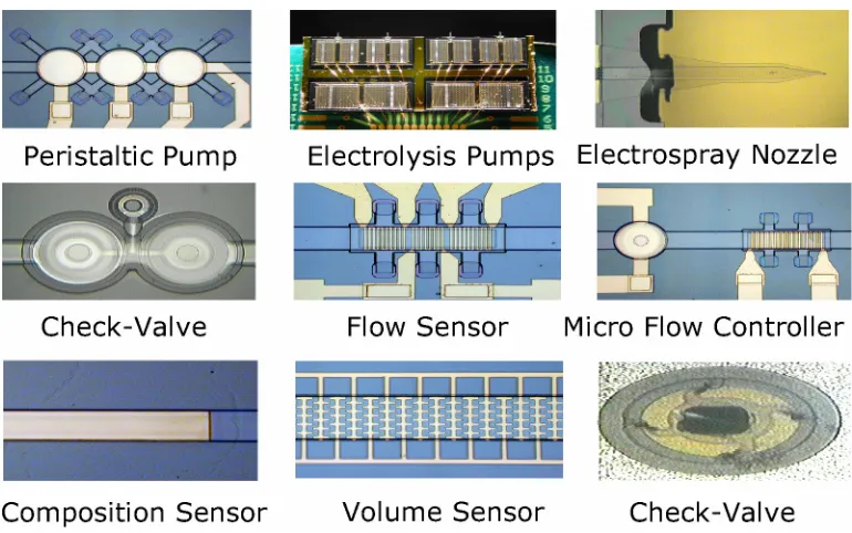
Figure 3-2 One-shot pump and valve using expandable microspheres ... 62
Figure 3-3 Multi-analyte sensor using specially-coated beads ... 63
Figure 3-4 Pictures illustrating the major steps for integrating beads into parylene channel ... 64
Figure 3-5 Process flow for the testing device for bead integration technology ... 65
Figure 3-6 Spin rate effect on the coated photoresist-bead film... 66
Figure 3-7. Spin-coated photoresist-bead film and the mixing ratio effect ... 67
Figure 3-8 Patterned bead-photoresist mixture film ... 68
Figure 3-9 Scanning electron microscopic pictures of patterned bead-photoresist films. 69 Figure 3-10 Beads sticking to subsequent parylene cover or to the substrate ... 70
Figure 3-11 Parylene thickness effect ... 70
Figure 3-12 Photoresist releasing issue... 72
Figure 3-13 Polymer-assisted particle aggregation... 72
Figure 3-14 Fabricated device pictures of the LC-ESI chip ... 74
Figure 3-15 Fabrication process flow for the liquid chromatography – electrospray ionization (LC-ESI) chip with integrated bead-column... 76
Figure 3-16 Fluorescent diagnostic technique ... 79
Figure 3-17 The photoresist releasing issue in various forms ... 80
Figure 3-18 Schematics of the packaging jig for the microchip... 82
Figure 3-19 Snapshots of released beads moving with liquid in a micro-channel ... 83
Figure 3-20 Snapshots of packing a column and electrospray to a mass spectrometer.... 83
Figure 3-21 Picture of a conventional externally-packed capillary LC column and ESI nozzle ... 86
column and ESI nozzle ... 88
Figure 3-24 MS spectrum for an LC separation of digested cytochrome c using a capillary column packed with photoresist-contaminated-then-cleaned C18 beads ... 90
Figure 4-1 Illustration of parylene trench-anchoring and roughening-anchoring ... 97
Figure 4-2 Cross-sectional pictures of a trench-anchored parylene channel ... 98
Figure 4-3 Top view picture of a roughened moat surrounding a photoresist channel... 99
Figure 4-4 Some of the existing coupling techniques... 100
Figure 4-5 Exploded view of the packaging scheme ... 101
Figure 4-6 Illustration and picture of the packaging after assembly... 102
Figure 4-7 Chemical structure of PEEK (polyether-ether-ketone) ... 102
Figure 4-8 Jig holes configuration ... 103
Figure 4-9 Top view picture of the device used in the pressure rating testing ... 104
Figure 4-10 Roughening-anchored channel before and after failure at high pressure.... 106
Figure 4-11 Trench-anchored channel before and after failure at high pressure ... 106
Figure 4-12 Cross-section of a sealed micro electrolysis actuation chamber... 108
Figure 4-13 Top view of a self-sealing electrolysis actuator ... 109
Figure 4-14 Pictures of the sealed micro electrolysis actuator ... 110
Figure 4-15 Snapshots of activation and deactivation of the actuator filled with DI water ...111
Figure 4-16 Snapshots of activation and deactivation of the actuator filled with 10% of acetonitrile in DI water ... 112
Figure 4-17 Snapshots of activation and deactivation of the actuator filled with 10% of methanol in DI water ... 113
Figure 4-18 Top view picture and cross-sectional illustration of the high-pressure electrolysis device... 114
Figure 5-1 Brita ion-exchange filter ... 121
Figure 5-2 (a) Fluorescent overview picture of the integrated ion chromatography chip before column packing. (b) Optical picture of the device after bead packing... 126
Figure 5-3 3D illustration of the device... 126
Figure 5-4 Illustration of the ion chromatography chip... 127
Figure 5-5 Illustrations of on-chip injection, separation, and detection of the ion chromatography chip ... 127
Figure 5-6 Configurations of the interdigitated electrodes in the conductivity detector cell ... 132
Figure 5-7 Common anions separation using a commercial HPLC system ... 135
Figure 5-8 Fabrication process flow ... 141
Figure 5-9 Illustration and pictures of the fabricated device after bead packing... 142
Figure 5-10 Packaged chip after wire bonding ... 143
Figure 5-11 Anion exchange beads used in the column packing... 144
Figure 5-12 Pressure–flow rate curve for an on-chip packed column ... 146
Figure 5-13 Conductivity detector cell equivalent circuit ... 147
Figure 5-14 Theoretical impedance frequency response ... 148
Figure 5-15 Impedance frequency spectrum of the mobile phase solution in contact with the on-chip interdigitated platinum electrodes... 149
Figure 5-16 Chromatogram of an on-chip ion chromatographic separation of seven anions ... 150
Figure 6-1 Overview of the HPLC-ESI/MS microchip before and after bead packing.. 158
Figure 6-2 Fabrication process flow for the chip... 161
Figure 6-3 Cross-sectional pictures of the fabricated device. The parylene microfluidic channels are anchored to the silicon substrate, greatly improving its pressure rating.... 162
Figure 6-6 Bubbling in the photoresist channels during parylene etching ... 164
Figure 6-7 Samples with no parylene coating appear intact after baking 10 minutes at 180 °C ... 166
Figure 6-8 Samples with parylene coating generate bubbles in the channels immediately after being heated at 170 °C... 166
Figure 6-9 Samples with 5 hours of extra baking before parylene coating, baked for 10 minutes at 180 °C... 167
Figure 6-10 Silicon needles at the bottom of trench ... 168
Figure 6-11 Packaging for the chip... 169
Figure 6-12 Pressure vs. flow rate testing result for the on-chip packed column... 172
Table 1-1 A selected list of properties for parylene N, C, and D ... 13
Table 2-1 Milestones in the history of HPLC development ... 24
Table 2-2 Typical sensitivity data for common HPLC detectors ... 43
Table 2-3 Nomenclature for HPLC systems ... 47
Table 3-1 Summary of an on-chip column properties ... 85
Table 4-1 Summary of the pressure testing results ... 105
Table 5-1 Limiting equivalent ionic conductances in aqueous solution at 25 °C... 129
C
HAPTER
1
INTRODUCTION
1.1 From IC to MEMS
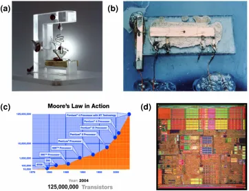
months [1, 2]. This predication is now known as Moore’s law. The law has become enormously influential for the semiconductor industry, which continues to develop better, cheaper, and smaller chips following the roadmap set by Moore (Figure 1-1 (c)). The state-of-the-art CPU chip, Intel’s Pentium 4 (Figure 1-1 (d)), already integrates 125 million transistors. It is really amazing that those primitive devices (Figure 1-1 (a) (b)) could grow into such a giant dynamic semiconductor industry, which has changed fundamentally how we live, think, and communicate, and will continue to do so for years to come.
Figure 1-1 (a) The first transistor (Bell Labs); (b) The first integrated circuit (Texas Instruments); (c) Moore’s law (Intel); (d) State-of-the-art CPU chip Pentium 4 (Intel).
[image:22.612.108.470.309.587.2]mechanical and later fluidic devices, which led to the fields of MEMS (Micro-Electro-Mechanical Systems) and µTAS (Micro Total Analysis Systems).
1.2 Micro-Electro-Mechanical
Systems
1.2.1 Introduction
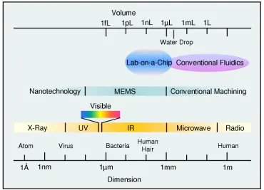
[image:23.612.139.509.396.663.2]A Micro-Electro-Mechanical System (MEMS) is a microfabricated system that contains both electrical and mechanical components. Its characteristic dimensions, as shown in Figure 1-2, range from 100 nm to millimeters. MEMS are also called micromachines or microsystems technology (MST). MEMS devices serve as one of the bridges connecting the digital world of the integrated circuits with the analog physical world.
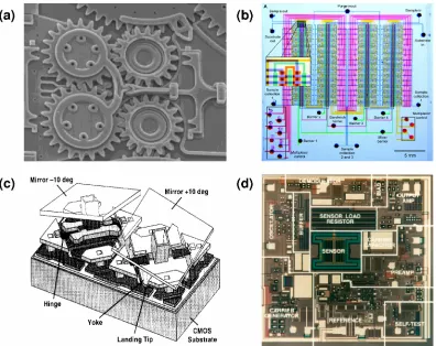
In 1959, Richard Feynman gave his famous speech titled “There’s plenty of room at the bottom,” in which he mapped out the tremendous potentialities for the miniaturization of machines [3]. In 1965, arguably the first MEMS device, a resonant gate transistor, was demonstrated [4]. In 1982, Kurt Peterson’s groundbreaking paper “Silicon as a mechanical material” [5] summarized many developments to that date, which greatly increased the awareness of MEMS and served as the starting point for realizing Feynman’s dreams. In 1989, researchers at University of California, Berkeley demonstrated the first IC-processed electrostatic micro-motors [6, 7], after which a wide variety of MEMS devices, technologies, and applications blossomed, and the field developed rapidly ever since [8]. Although their complexities are still far from those of state-of-the-art ICs, MEMS devices have shown many hallmarks of ICs such as multi-level stacking (Figure 1-3 (a)) and large-scale integration (LSI) (Figure 1-3 (b)) [9]. MEMS devices also achieved remarkable commercial successes, such as inkjet printer heads from Hewlett Packard, pressure sensors from Honeywell and Motorola, Digital Light Processing (DLP) system from Texas Instruments (Figure 1-3 (c)), and accelerometers from Analog Devices (Figure 1-3 (d)).
1.2.2 Advantages
downsizing, in the microscopic world, for instance, gravity is no longer important; surface effects dominant; thermal time constant is minimized; and fluids behave as laminar flows. Moreover, the per-unit cost is low due to MEMS batch fabrication. In addition, MEMS offers new functions that never have been possible before. Its future is even more exciting considering its ability to integrate with ICs.
[image:25.612.128.524.238.552.2]
Figure 1-3 Famous MEMS devices. (a) Multi-level MEMS gears (Sandia National Lab); (b) Large-scale integration of miniature pumps and valves; (c) Digital micro-mirror device for digital light processing (Texas Instruments); (d) Monolithic accelerometer
1.2.3 Fabrication Technologies
Because of its root in the IC industry, many of MEMS basic processing techniques are borrowed or adapted from those used to produce ICs, such as photolithography, oxidation, diffusion, ion implantation, chemical vapor deposition (CVD), evaporation, sputtering, wet chemical etching, and dry plasma etching [10]. Many microfabrication techniques specifically for MEMS have also been developed over the years, such as KOH, DRIE (deep reactive-ion-etching), LIGA (German acronym for x-ray lithography, electroforming, and molding), wafer bonding, electroplating, and 3D stereo lithography [11]. In recent years, polymer MEMS have become popular, resulting in many new techniques suitable for polymers, for instance soft lithography [12–14].
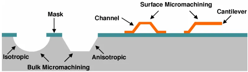
Multiple basic microfabrication processes are combined to make complete devices in two general ways, bulk micromachining [15] and surface micromachining [16]. As illustrated in Figure 1-4, bulk micromachining uses chemical or plasma selective etching of substrate material, with the help of masking films, to form structures in the substrate. The etching process can be either isotropic such as HNA (hydrofluoric acid + nitric acid + acetic acid), XeF2, or anisotropic such as KOH, TMAH
Figure 1-4 Illustration of bulk micromachining and surface micromachining.
1.2.4 From MEMS to µTAS
Although MEMS started in the mechanical world, the field soon grew rapidly to encompass a wide spectrum of applications in many sub and spin-off fields, such as MOEMS (Micro-Optical-Electro-Mechanical System), RF-MEMS, and µTAS (Micro Total Analysis Systems). At the present time, µTAS is the one of the fastest growing subfields, which is highly interdisciplinary by nature, covering areas such as microfluidics, material science, analytical chemistry, and biotechnology.
1.3 Microfluidics, Lab-on-a-Chip, and µTAS
1.3.1 Introduction
Microfluidics generally refers to the science and technology of manipulating
minute amounts of fluids with volumes ranging from micro liters (1 µL = (1 mm) ) to 3
pico liters (1 pL = (10 µm) ) (Figure 1-2). Lab-on-a-chip is the miniaturization and 3
microfluidic system that can automatically carry out all the necessary functions to transform chemical information into electronic information. Microfluidics is a more general term than µTAS.
The concept of µTAS was first suggested by Manz in 1990 [17], although the first µTAS device, a miniaturized gas chromatography system, was demonstrated in 1979 [18]. Today, µTAS has grown tremendously into a large dynamic multidisciplinary field, whose impact could be far-reaching and revolutionary. The field is extensively reviewed in several papers from Manz’s group [19–21].
The advantages of µTAS include significantly reduced size (portability), power consumption, sample and reagent consumption, and manufacture and operating costs (disposability). In addition, µTAS can achieve better performance in terms of speed, throughput, mass sensitivity, and automation.
It should be noted, however, unlike its integrated circuit analog, which emphasizes continuous reduction of transistor size, µTAS focuses on making more complex systems with more sophisticated fluid handling capabilities, rather than pushing for the smallest micro-channels possible.
1.3.2 Future Challenges
After over a decade of research and development on µTAS, it is interesting to discuss its pressing issues and future challenges. The most important ones are sample preparation, world-to-chip interfacing, on-chip chromatographic separation, on-chip feedback control, detection, and total integration.
The integration of sample preparation into microfluidic devices represents one of the main hurdles towards achieving true functional lab-on-a-chip. It becomes more challenging for the enormous variation in samples to be analyzed, and/or the complex raw material in the environment. This problem may have to be handled on a case by case basis. Two reviews on sample preparation in microfluidic systems are given in [22, 23].
Even with preprocessed samples, coupling of the samples, reagents, and conventional macro-scale tubing to the chips, often referred to as “world-to-chip interfacing,” remains a difficult problem. Although the chip may only need a nano liter sample, it is impossible for conventional scale fluidics to handle such a small amount. A much larger volume has to be started with, unless the chip can acquire a nano liter sample from its environment directly. Coupling conventional-scale fluidics with microfluidics is also challenging, especially since no packaging standard is set. Microfluidic chips are usually small and thin, which makes most conventional coupling techniques unrealistic. New coupling methods that are not significantly larger than the chip need to be developed [24]. Especially for high-pressure applications, such as liquid chromatography, reliable coupling with high-pressure ratings is highly desired.
of integration for a complete on-chip system. Liquid chromatography, further discussed in Chapter 2, is the most important separation technique in analytical chemistry. It essentially eliminates highly specific sensing, which is very difficult to achieve.
On-chip feedback control is not widely implemented even today, although its importance is starting to be realized. Conventional transducers are not sensitive enough or practical for monitoring on-chip flows and reactions. It is highly desirable and useful to know the operating conditions of the chip in real time. Devices based on silicon or glass would be better than those based on PDMS (polydimethylsiloxane), since it is much easier to integrate electrodes and circuits on silicon or glass substrates.
Optical detection does not scale down well. With miniaturization of the micro-channels, the usable optical path is greatly reduced, which leads to a significantly reduced optical signal and thus lower sensitivity for optical techniques, such as UV absorbance. Selectivity is also a serious issue. For conventional analysis, selectivity is usually accomplished through chromatography-based separation prior to detection. However, on-chip liquid chromatography is highly underdeveloped, limiting the ability to separate sample compounds on-chip and hence limiting selectivity. Furthermore, many of today’s detectors are still off-chip, especially those based on optics and mass spectrometry. When the detector is significantly larger than the chip itself, the whole setup is far from a real “lab-on-a-chip.”
inefficient, unreliable, and costly. The integration process is not trivial at all. Firstly, most individual devices are built with incompatible technologies. The desired approach would be to micromachine every part in a compatible way. Secondly, there are few technologies that are sufficiently versatile to make the wide variety of devices needed for the system, while still powerful enough to keep each device optimized. Parylene microfluidics technology, as described in the next section, is a great candidate.
1.4 Parylene
Microfluidics
Technology
1.4.1 Introduction to Parylene
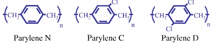
[image:31.612.136.510.538.617.2]Parylene (poly-para-xylylene) is the generic name for members of a unique vapor phase deposited thermoplastic polymer series. Discovered in 1947 and commercialized by Union Carbide Corporation in 1965, parylene is used in several industries because of its superior properties. The primary application is PCB (printed circuit board) coating in the electronics industry, where parylene protects the delicate electronic devices against moisture and corrosive environments. Figure 1-5 shows the chemical structures for the three most commonly used parylene types: parylene N, parylene C, and parylene D.
Figure 1-5 Chemical structures of parylene N, C, and D.
barrier to gas and moisture. The gas permeability of parylene is more than four orders of magnitude smaller than that of PDMS (polydimethylsiloxane), which is another popular material for microfluidic devices. Moisture vapor transmission is ten times less than silicones.
Parylene is extremely inert to most chemicals and solvents. Based on the manufacturer’s study [25], solvents have minor swelling effect on parylene N, C, and D with a 3% maximum increase in film thickness. The swelling is found to be completely reversible after the solvents are removed by vacuum drying. Inorganic reagents, except for oxidizing agents at elevated temperatures, have little effects on parylene. Parylene is also biocompatible (USP Class VI), which means it is safe for long-term human implants. Parylene exhibits impressive mechanical strength and flexibility in a thin film coating. Its Young’s modulus is between silicon and PDMS, so it can be used to make both rigid structures and flexible actuators.
Parylene is an excellent electrical insulator as well as a good thermal insulator. For example, the breakdown voltage for 1 µm thick parylene is over 200 volts, and the thermal conductivity of parylene C is only four times that of air (0.21 mW/(cm·K)).
Optically, parylene is transparent in the visible light range. It only absorbs light under 280 nm in wavelength, which unfortunately limits its UV applications.
Moreover, deposition of parylene C is faster than the other two. Parylene C is the parylene of choice for most conventional and microfluidic applications.
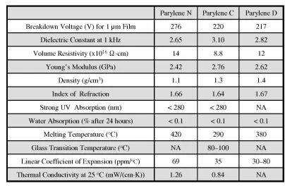
[image:33.612.118.522.220.484.2]Detailed electrical, mechanical, thermal, barrier, optical, and other properties can be found on a parylene vendor’s website [26]. A list of selected properties for parylene N, C, and D are shown in Table 1-1.
Table 1-1 A selected list of properties for parylene N, C, and D.
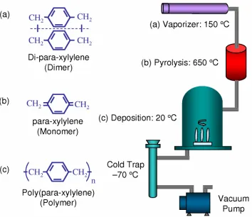
deposition chamber, the monomers reunite on all exposed surfaces in the form of polymers (poly-(para-xylylene)). The deposition takes place at molecular level. The monomers are extremely active molecules having mean free path on the order of 1 mm (under deposition pressure of around 100 mTorr), which results in superior penetration power and a high degree of conformability to the surfaces being coated. The coated substrate temperature never rises more than a few degrees above ambient. Additional components of the system include a mechanical vacuum pump and associated cold trap. Although parylene N structure is used in Figure 1-6, the process is almost identical for all three common types of parylene, except for some slight differences in pyrolysis temperature and deposition pressure.
Typical coating thickness ranges from one to tens of microns. It can also be as thin as hundreds of angstroms. The coating thickness can be controlled by the amount of dimer used. The normal deposition rate of parylene C is about 5 µm per hour. The deposition rate is directly proportional to the square of the monomer concentration and inversely proportional to the absolute temperature [26]. Higher deposition rates, however, can result in poor film quality, which often appears as a milky (cloudy) film in contrast to normal clear transparent ones.
1.4.2 Parylene Technology for Liquid Chromatography On-a-Chip
Besides its superior properties, parylene is well suited for µTAS applications because of its ease of integration with other microfabrication techniques.
Parylene’s room-temperature deposition makes it post-CMOS compatible, which allows parylene devices to have electrodes, sensors, and even circuits. Parylene’s conformal coating enables it to form complicated structures with great step coverage. Moreover, parylene is bio-compatible which makes it suitable for biological sensing applications and implant devices. As an organic polymer, parylene can be easily etched with oxygen plasma, using photoresist or metal as a mask.
Figure 1-7 Parylene microfluidic devices.
1.5 Bibliography
[1] G. E. Moore, "Cramming more components onto integrated circuits" (Reprinted from Electronics, p. 114–117, April 19, 1965). Proceedings of the IEEE, 1998. 86(1): p. 82–85.
[2] G. E. Moore, "Cramming more components onto integrated circuits." Electronics, 1965. 38(8): p. 114–117.
[3] R. P. Feynman, "There's plenty of room at the bottom." Journal of Microelectromechanical Systems, 1992. 1(1): p. 60–66.
[4] H. C. Nathanson, W. E. Newell, R. A. Wickstrom, and J. J. R. Davis, "The resonant gate transistor." IEEE Trans. Electron Devices, 1967. 14(3): p. 117– 133.
[5] K. E. Petersen, "Silicon as a mechanical material." Proceedings of the IEEE, 1982. 70(5): p. 420–457.
[6] L.-S. Fan, Y.-C. Tai, and R. S. Muller, "IC-Processed electrostatic micromotors." Sensors and Actuators, 1989. 20(1–2): p. 41–47.
[7] Y.-C. Tai and R. S. Muller, "IC-Processed electrostatic synchronous micromotors." Sensors and Actuators, 1989. 20(1–2): p. 49–55.
[8] G. T. A. Kovacs, Micromachined transducers sourcebook. McGraw-Hill series in electrical and computer engineering. 1998. Boston: WCB/McGraw-Hill.
[9] T. Thorsen, S. J. Maerkl, and S. R. Quake, "Microfluidic large-scale integration." Science, 2002. 298(5593): p. 580–584.
[11] M. J. Madou, Fundamentals of microfabrication : the science of miniaturization. 2nd ed. 2001. Boca Raton, Fla.: CRC Press.
[12] Y. N. Xia and G. M. Whitesides, "Soft lithography." Annual Review of Materials Science, 1998. 28: p. 153–184.
[13] G. M. Whitesides, E. Ostuni, S. Takayama, X. Y. Jiang, and D. E. Ingber, "Soft lithography in biology and biochemistry." Annual Review of Biomedical Engineering, 2001. 3: p. 335–373.
[14] J. C. McDonald, D. C. Duffy, J. R. Anderson, D. T. Chiu, H. K. Wu, O. J. A. Schueller, and G. M. Whitesides, "Fabrication of microfluidic systems in poly(dimethylsiloxane)." Electrophoresis, 2000. 21(1): p. 27–40.
[15] G. T. A. Kovacs, N. I. Maluf, and K. E. Petersen, "Bulk micromachining of silicon." Proceedings of the IEEE, 1998. 86(8): p. 1536–1551.
[16] J. M. Bustillo, R. T. Howe, and R. S. Muller, "Surface micromachining for microelectromechanical systems." Proceedings of the IEEE, 1998. 86(8): p. 1552–1574.
[17] A. Manz, N. Graber, and H. M. Widmer, "Miniaturized total chemical analysis systems. A novel concept for chemical sensing." Sensors and Actuators, B: Chemical, 1990. B1(1–6): p. 244–248.
[19] D. R. Reyes, D. Iossifidis, P. A. Auroux, and A. Manz, "Micro total analysis systems. 1. Introduction, theory, and technology." Analytical Chemistry, 2002. 74(12): p. 2623–2636.
[20] P. A. Auroux, D. Iossifidis, D. R. Reyes, and A. Manz, "Micro total analysis systems. 2. Analytical standard operations and applications." Analytical Chemistry, 2002. 74(12): p. 2637–2652.
[21] T. Vilkner, D. Janasek, and A. Manz, "Micro total analysis systems. Recent developments." Analytical Chemistry, 2004. 76(12): p. 3373–3386.
[22] A. J. de Mello and N. Beard, "Dealing with 'real' samples: sample pre-treatment in microfluidic systems." Lab on a Chip, 2003. 3(1): p. 11N–19N.
[23] J. Lichtenberg, N. F. de Rooij, and E. Verpoorte, "Sample pretreatment on microfabricated devices." Talanta, 2002. 56(2): p. 233–266.
[24] E. Meng, S. Y. Wu, and Y.-C. Tai, "Silicon couplers for microfluidic applications." Fresenius Journal of Analytical Chemistry, 2001. 371(2): p. 270– 275.
[25] Specialty Coating Systems, "Solvent resistance of the parylene." Trade literature.
[26] http://www.scscookson.com/parylene_knowledge/specifications.cfm
[28] J. Xie, Y. Miao, J. Shih, Q. He, J. Liu, Y.-C. Tai, and T. D. Lee, "An electrochemical pumping system for on-chip gradient generation." Analytical Chemistry, 2004. 76(13): p. 3756–3763.
[29] X.-Q. Wang and Y.-C. Tai, "Normally closed in-channel micro check valve." Proceedings of the 13th IEEE International Conference on Micro Electro Mechanical Systems (MEMS 2000). Miyazaki, Japan, 2000. p. 68–73.
[30] J. Xie, X. Yang, X.-Q. Wang, and Y.-C. Tai, "Surface micromachined leakage proof parylene check valve." Proceedings of the 14th IEEE International Conference on Micro Electro Mechanical Systems (MEMS 2001). Interlaken, Switzerland, 2001. p. 539–542.
[31] J. Xie, J. Shih, and Y.-C. Tai, "Integrated surface-micromachined mass flow controller." Proceedings of the 16th IEEE International Conference on Micro Electro Mechanical Systems (MEMS 2003). Kyoto, Japan, 2003. p. 20–23. [32] H. S. Noh, P. J. Hesketh, and G. C. Frye-Mason, "Parylene gas chromatographic
C
HAPTER
2
NANO HPLC
2.1 High-Performance Liquid Chromatography
2.1.1 Introduction
High-Performance Liquid Chromatography (HPLC) is one of the most powerful, versatile, and widely-used separation techniques. It allows separation, identification, purification, and quantification of the chemical compounds in complex mixtures. It is an indispensable tool in analytical chemistry. It has a wide spectrum of applications in fields such as the pharmaceutical industry, proteomics, the chemical industry, environmental laboratories, the food industry, forensic analysis, and clinical analysis. The only limitation for HPLC is that the sample must be soluble in the liquid phase.
stationary, while the other phase is mobile. When this mobile phase is liquid, the chromatographic technique is called Liquid Chromatography (LC). The LC stationary phase can be either solid or surface functional groups bonded on a solid. High-performance liquid chromatography is comprised of those LC techniques that require the use of elevated pressures to force the liquid through a packed bed of stationary phase, which is highly-efficient for separation. The packing material usually consists of particles with dimensions around 10 µm, which creates a large backpressure in the densely-packed bed. Therefore, the technique is also called high-pressure liquid chromatography.
In short, during the elution process, the surface functional groups (stationary phase) on the particles interact with the sample and eluent (mobile phase). When the injected sample plug is carried through the column by the liquid eluent, different sample components interact with the stationary phase differently, partitioning their time in the stationary and mobile phases, and therefore migrate through the column at different speeds, and exit the column at different times. This process is illustrated in Figure 2-1.
Figure 2-1 Illustration of the chromatographic separation process.
can be problematic. Early peaks usually have poor resolution and final peaks are broad and flat. Weaker solvents will improve early peaks but worsen the final peaks, while stronger solvents further compress early peaks but improves final peaks. This so-called “general elution problem” can be solved by starting with a weak solvent then gradually increasing solvent strength over time, so that all peaks can be well resolved. The gradient profile can be best determined empirically.
2.1.2 History
Chromatography was invented by a Russian botanist Mikhail Tswett (1872–1919) in 1903 (Figure 2-2) [2]. He employed the technique to separate plant pigments by passing solutions of these species through glass columns packed with finely divided calcium carbonate [3]. The separation appears as colored bands on the column, which is why he named this technique chromatography. The word chromatography is composed of two Greek roots, chroma (color) and graphein (to write).
Figure 2-2 The inventor of chromatography, Tswett, and his chromatographic device.
mathematics to describe the separation process [5], which became the basis for modern HPLC. They shared the Nobel Prize in Chemistry (1952) for their invention of partition chromatography [6]. Martin also published the first application of gas chromatography with James in 1952. In the same year, gradient elution was demonstrated by Alm. By the late 1960s, LC theories and instrumentations were well established, which led to the first commercially available liquid chromatography system in 1969. Around 1973, packing technologies were advanced so that, for the first time, reproducible high-efficiency columns could be prepared with particles less than 10 µm in diameter. Also in 1973, modification of silica surface via silanization became commercially feasible. These breakthroughs led to the first 10 µm reversed-phase HPLC columns [1]. Since then, HPLC has become one of the most important and fastest-growing techniques in the modern laboratory. The state-of-the-art column liquid chromatography equipment and instrumentation is discussed in a recent review [7].
2.1.3 Theory
2.1.3.1 Chromatogram and Important Equations
The separated compounds appear as peaks in the chromatogram (Figure 2-3), which is a plot of some function of the compound concentrations versus elution time. Each peak is a Gaussian curve in theory. Retention time of a peak is defined as the time
between sample injection and the peak maximum. t0 is the retention time of the
unretained sample, which is the time that the mobile phase takes to travel through the
column, also called breakthrough time. If the column length is Lc and the mobile phase linear flow velocity is u, then
0 c
L t
u
[image:45.612.131.520.349.658.2]= (2.1)
For most LC separations regardless of column dimension, the optimized linear flow velocity u is on the order of 1 mm/s, as a rule of thumb. The corresponding volumetric flow rateF is:
c
F =εuA (2.2)
where Ac is the column cross-sectional area and ε is the column porosity. For cylindrical columns with inner diameter (ID) of dc:
2
4 c c
d A =π
(2.3) The column porosity ε is:
column packing column
V V
V
ε = −
(2.4) where Vcolumn is the total volume in the column and Vpacking is the volume taken up by the
solid packing material in the column. The column porosity can also be expressed as the sum of inter-particle porosity and inner-particle porosity.
R
t is the retention time of a retained compound. Two compounds can be separated if they have different retention times. '
R
t is the net/adjusted retention time relative to t0. Therefore,
' 0
R R
t = +t t (2.5)
0
t represents the time a compound spends in the mobile phase, which is identical for all compounds since compounds only move down the column when they are in the mobile
phase. '
R
t represents the time spent in the stationary phase. The longer a compound stays
To characterize a compound, the retention factor, k, is preferred over the retention time, since the latter also depends on column length and flow velocity. kis given as:
'
0
0 0
R R t t t
k
t t
−
= = (2.6)
kis independent of column length and flow rate and represents the molar ratio of the compound staying preference between the stationary and the mobile phase. Therefore,
k can be also expressed as:
stationary mobile n k
n
= (2.7)
where nstationary and nmobile represent the number of molecules of a certain compound in the stationary and mobile phases respectively. Various compounds must have different k values in order to be separated.
The separation factor, α , is defined as:
2 2 1 1 ( ) k k k k
α = > (2.8)
The separation factor shows the chromatographic system’s separation power between two compounds, i.e., its selectivity.
As shown in Figure 2-3, w is the peak width. When measured at 13.4% height of a Gaussian peak, w equals four times the standard deviation, σ , of the peak. The resolution, R, of two peaks is defined as the ratio of the two-peak maxima distance to the mean of the two peak widths:
2 1
1 2
2tR tR
R
w w
− =
The more separated and sharp (narrow) the two peaks are, the higher the resolution. The number of theoretical plates,N, can be calculated from the chromatogram:
2
16
( )
tRN
w
= (2.10)
The equation is correct only if the peak has a Gaussian shape, otherwise, some other approximate equations should be used. Since the calculation of N involves retention time, N can only be derived from isocratic, not gradient, chromatograms. The plate number obtained from a non-retained peak is a measure of the column packing efficiency. HigherN and higher efficiency can be obtained with longer columns, smaller beads, better packing, and better optimized flow velocity. N is proportional to column length, and inversely proportional to bead diameter dp:
N∝Lc (2.11)
1 N
p d
∝ (2.12)
Qualitative and quantitative information about the sample components can be obtained from the chromatogram. The retention time of a compound is always the same under identical chromatographic conditions. Therefore, a compound peak can be identified by comparing to a standard chromatogram with known compounds. The concentration of a compound can be determined by its peak height, which is proportional to the injection concentration. Plots of peak height versus injection concentration, usually linear, can be obtained using samples with known component concentrations.
2
p c
Pd L uη
∆ Φ =
(2.13) where ∆P is the pressure drop across the column, Lc is the column length, η is the
viscosity of the mobile phase. Φ is between 500 (spherical beads) and 1000 (irregular beads) for columns packed with totally porous materials. This equation can also be rearranged to estimate column backpressure:
2 c p L u P d η Φ ∆ = (2.14)
2.1.3.2 Band Broadening and van Deemter Equation
Chromatographic bands increasingly broaden as the bands move down the column (Figure 2-4). Band broadening reflects a loss of column efficiency. There are four reasons for band broadening.
Figure 2-4 Illustration of band broadening during chromatographic elution.
The second is flow distribution of the mobile phase traveling in the channels between the beads (Figure 2-5 (b)). The laminar flow is faster in the channel center and slower on the edge. Both of the above effects can be reduced by using more uniformly-sized beads. However, the mobile phase flow velocity has little effect for either one.
The third cause is longitudinal diffusion of sample molecules in the mobile phase (Figure 2-5 (c)), which happens only when small beads are used, mobile phase velocity is low, and the sample diffusion coefficient in the mobile phase is large. This effect can be minimized by choosing an adequate mobile phase velocity.
Figure 2-5 Four mechanisms of band broadening.
The forth cause is the time-consuming mass transfer process between mobile, “stagnant mobile,” and stationary phases (Figure 2-5 (d)). Inside the pores of the beads, molecules move only by diffusion. Therefore, some molecules could be stuck in the pores while others continue to move down the column with mobile phase. In this case, the higher the mobile phase flow velocity, the more broadening effect will be.
In summary, the theoretical plate heightH(explained in detail in Section 2.1.3.4),
representing the column efficiency, can be plotted against mobile phase velocity u
flow distribution is shown with line 1. The longitudinal diffusion effect is shown with line 2. The mass transfer effect is shown with line 3. And the van Deemter curve is line 4,
which is the summary of all four effects. The optimal u is reached when the
correspondingHreaches minimum. This H–u relationship can also be expressed with the following van Deemter equation.
B
H A Cu
u
= + +
(2.15) where A B, , and C are coefficients for eddy-diffusion and flow distribution effects,
longitudinal diffusion effect, and mass transfer effect respectively.
Figure 2-6 Van Deemter Curve.
2.1.3.3 Band Broadening vs. Separation
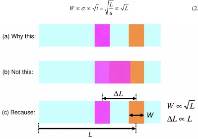
proportional to the traveled length. This is the fundamental reason why chromatography works [1].
Chemical compound concentration is not uniform in a band (peak). The band is rather a statistical distribution of molecules. The width of the band is always proportional to the standard deviation of the distribution, σ , with the proportionality factor depending on the distribution type. For typical chromatographic bands that are Gaussian distributed,
the peak width measured at 13.4% of peak height is 4σ. The band standard deviation
increases with the square root of the time spent in the column. Therefore, as equation (2.16) shows, the band width W increases with square root of L, the length traveled.
L
W t L
u
σ
[image:52.612.88.487.341.621.2]∝ ∝ = ∝ (2.16)
Figure 2-7 Band broadening effect vs. separation effect.
1 2 1 2
(R R ) ( )
c
L
L t t u k k L L
L
∆ = − = − ∝ (2.17)
2.1.3.4 Height Equivalent to a Theoretical Plate
In some sense, the height equivalent to a theoretical plate (HETP), H, can be imagined to be the distance over which chromatographic equilibrium is achieved [8]. The smaller the H value, the higher the column efficiency. However, the plate model is not a very good presentation of chromatographic column; plate height represents column efficiency for historic reasons only, and not because it has physical significance [3].
Chromatographic band (peak) width can be described by its variance σ2. As
stated in the previous section, σ increases with the square root of the length traveled. Therefore, the peak variance increases linearly with the length it has traveled (Figure 2-8). The smaller the slope, the slower the peak widens, the higher the column efficiency. The slope (variance per unit length) is defined to be HETP:
2
H L
σ
≡ (2.18)
Hcan also be calculated as:
c
L H
N
= (2.19)
The reduced/dimensionless plate height, h, is defined as:
h represents the number of layers of stationary phase packing over which a complete
chromatographic equilibrium is obtained. A column with good packing usually has h
from 2 to 5.
Figure 2-8 Definition of HETP.
2.1.4 Instrumentation
[image:54.612.213.364.173.306.2]A typical HPLC instrument has the following parts: solvent reservoirs, high-pressure pumps, sample injection device, separation column, and detector (Figure 2-9). Some of the optional parts are guard column, thermostat oven, and fraction collector. Since this thesis work emphasizes column and detector, these two parts will be discussed in more detail below.
2.1.4.1 Solvents
Solvents must be HPLC-grade. They have to be degassed before entering the column, otherwise gas bubbles will appear in the detector where the pressure is low. Commercial HPLC systems usually have on-line degassers in their pumping units. The most preferred organic solvent is now acetonitrile rather than methanol mainly because the latter is more viscous, and thus generates higher backpressure. Methanol viscosity is 0.6 cP at 20 °C, while that of acetonitrile is 0.37 cP. Acetonitrile is, however, much more expensive than methanol.
2.1.4.2 Pumps
An HPLC pump has to be able to generate thousands of psi pressure, and provide high flow accuracy and precision. The delivered flow rate must be unaffected by backpressure change during separation. For example in gradient separations, the ratio between solvents in the mobile phase changes, which leads to a total effective viscosity change, and therefore a backpressure change. Commercial HPLC pumps are mostly piston pumps. Recently, a new pump for nano HPLC applications has appeared on the market, which uses compressed air as the pressure source and a flow sensor to perform feedback control to generate precise nano liters per minute flow rates [9].
2.1.4.3 Sample Injectors
sample injection inlet, from which sample is loaded into the loop. Excessive amount of sample is usually loaded, in order to make sure the loop is completely filled. Then the internal rotor seal is rotated to bring the sampling loop online with the pump and column (Figure 2-10 (b)) to inject sample into the column.
Figure 2-10 Injection valve working mechanism.
2.1.4.4 Chromatographic Columns
2.1.4.4.1 Column Dimension
2.1.4.4.2 Column Packing Physical Properties
HPLC columns are mostly densely-packed with micro-scale beads. The aim of the beads is to carry the stationary phase and to generate high surface area. As shown in Figure 2-11, the beads used in HPLC column packing differ in shape, size, pore size, and surface area (porosity).
Figure 2-11 Physical properties of liquid chromatographic beads.
The shape of HPLC beads is either spherical or irregular. The vast majority of all columns uses spherical beads, since they provide more uniform and dense packing, better flow profiles, less backpressure, and higher efficiency. Irregular beads often provide more surface area and higher capacity.
Pore size is the average dimension of the channels inside the porous beads. The bead internal structure is fully porous and can be best compared to a sponge with a rigid structure. Within the pores, the mobile phase and the analytes do not flow but move only by diffusion. The pore size can range from 60 Å to over 10,000 Å. Molecules smaller than the pore size can enter the pores and fully utilize the internal stationary phases. Larger molecules may be kept outside the pores and thus have little retention. In practice, molecular weight is used instead of size.
The bead surface area is determined by the pore size and abundance of pores in the bead. Higher porosity beads with smaller pores have larger surface area. For example, the surface area of a column packed with 5 µm non-porous beads is only 0.02 m2/mL, while that of a totally porous-bead-packed bed is 150 m2/mL [1]. Pores that are too small, however, are detrimental to column efficiency, since they are difficult to access. For general purpose columns, 10 nm pores are often used. For large molecules like proteins, 100 nm pores are the best choice. For beads without bonded surface functional groups, larger surface area means more capacity, longer retention, and generally higher resolution. For bonded beads, both surface area and bonding density should be considered. There are also non-porous bead columns, which can eliminate band broadening caused by poor mass transfer into the stagnant mobile phase within the pores, and can reduce undesired loading capacity in some cases.
2.1.4.4.3 Base Material and Bonded Phases
is the most popular base material for HPLC column packing, while polymeric materials are gaining popularity. Silica beads are produced by a number of different syntheses such as complete hydrolysis of sodium silicate, or the polycondensation of emulsified polyethoxysiloxane followed by dehydration [8]. A silica bead has silanol (-OH) groups on its surface, which can be chemically modified (replaced) with desired stationary phases. A number of reactions can be used. Figure 2-12 gives one example, where the silanol group is reacted with an alcohol, ROH. R may be an alkyl chain or other functional group.
Figure 2-12 Chemical modification of silica surface.
ODS (octadecylsilane), in which R= -(CH ) CH , is the most common type used 2 17 3 in HPLC columns. It is also called C18 since there are eighteen carbon atoms in this alkyl chain (Figure 2-13). It is very non-polar and is used in reversed-phase (RP) HPLC, as
explained in Section 2.1.4.4.4. Similarly, C8 (R= -(CH ) CH ) and C4 2 7 3
2 3 3
(R= -(CH ) CH ) are also used in RP-HPLC. Since they have shorter alkyl chains than C18, they are less non-polar and require less run time for separations.
Figure 2-13 Chemical structure and 3D illustration of C18 functional groups on silica surface.
Compared to silica beads, polymer materials have wider pH range. Silica can only tolerate mobile phases having pH 2 to 7.5, while polymers are usually good between pH 2 to 12, sometimes even 0 to 14. Strong acids and bases can not be used for silica-based columns. Polymer-based columns, on the other hand, can be thoroughly cleaned with strong acids or bases to have a longer lifetime than silica-based columns. Moreover, the polymer material surface is free of silanol group, which can sometimes affect separation.
2.1.4.4.4 Separation Mechanisms
The most common types of LC, based on the separation mechanisms in the column, are normal-phase, reversed-phase, ion, size-exclusion, hydrophilic interaction, and hydrophobic interaction.
Normal-phase LC employs a polar (water-soluble, hydrophilic) adsorbent such as silica, and a non-polar (fat-soluble, hydrophobic) mobile phase based on hydrocarbons such as petrol. It is also often called adsorption chromatography and was the first type of LC technique developed. However, two reasons greatly limit its use. Firstly, silica is hydrophilic, any trace amount of water in the solvent could change its surface property, thus change elution time. Second, many interesting analytes, such as amino acids, peptides and nucleotides, are so polar that they do not easily dissolve in non-polar solvents, and therefore can not be analyzed by normal-phase.
The solution to these two problems is to modify the silica surface to be hydrophobic (non-polar), and use polar solvents for elution, which is known as reversed-phase (RP) LC. RP-LC is the most popular type of LC today. Non-polar compounds are eluted later than polar compounds. Water as a mobile phase cannot interact with the non-polar (hydrophobic) station phase. Therefore, water has little elution power. Non-aqueous solvents, such as acetonitrile and methanol, are less polar than water. Therefore, they have better elution capability. The more solvent content in the mobile phase, the faster the separation.
Size-exclusion chromatography is a separation based on size, i.e. according to molecular mass, rather than any interaction phenomena. Larger analytes have limited access to stationary phase in the pores of the packing. Therefore, larger molecules are eluted earlier than smaller ones.
Hydrophilic interaction chromatography is an extension of normal-phase chromatography where very polar analytes and aqueous mobile phases are used. Stationary phases are still the same.
Some protein separations need significantly less-hydrophobic stationary phase to prevent the proteins from being denatured by common RP-HPLC solvents. This technique is called hydrophobic interaction chromatography, which is an extension of reversed-phase chromatography.
2.1.4.5 Detectors
The choice of the appropriate detector for an application depends mainly on the analytes of interest and the desired sensitivity. Table 2-2 summarizes the sensitivity for the most common HPLC detectors [3, 10–12]. The sensitivity data are dependent on the compound, instrument, and HPLC conditions. Those given in the table are only typical values. Other important detector properties include selectivity, response time, and detector cell volume. The selectivity determines how well it can discriminate a compound from others or from the background. The detector also has to be fast enough to allow real-time detection. If more time is required to achieve a desired sensitivity, the analyte fractions may have to be collected and analyzed later. Since trace levels of chemicals are to be determined, the volume of the detector cell needs to be small enough that the separated peaks do not distort or overlap in the detector.
Table 2-2 Typical sensitivity data for common HPLC detectors.
path is maximized to maximize absorbance that is proportional to the flow path in the detector cell. The absorbance rather than the transmittance is recorded, because the former, not the latter, is linear with sample concentration. The absorbance method is simple and reliable. However, it is less sensitive than fluorescence, electrochemical, and mass spectrometry detections. And it is not a universal method for all analytes.
Fluorescence detection captures the fluorescence emission at a higher wavelength generated by a lower excitation wavelength. The analytes must have fluorophores, which are compounds that fluoresce. This method has much better sensitivity and selectivity than most other methods. Its sensitivity comes from the fact that most background solvents do not fluoresce and the analytes usually strongly fluoresce. There are two reasons for its selectivity. Firstly, not all organic molecules fluoresce. Secondly, fluorescence detection uses two distinct wavelengths as opposed to one in absorbance method, which greatly reduces the chance of interfering peaks. One important disadvantage of fluorescence detection is the limited number of compounds that fluoresce, although some of them can be chemically derivatized to have fluorescent “tags.” Another drawback is that the fluorescent response can be affected by solvent type, temperature, and pH.
a property of the bulk solution, any change in temperature, pressure, or composition can affect the baseline stability. Therefore, gradient elution should be avoided.
Electrochemical detectors measure the electrochemical properties of the HPLC column effluents. It has good sensitivity and can be used for an extensive list of analytes. The most common type of electrochemical detectors is the conductivity detector, which measures the electrical conductance. It is especially used for ion chromatography where the analytes are ionic and have weak UV absorbance. Non-suppressed conductivity detection measures sample signals directly on top of baseline signal generated by the mobile phase. Suppressed detection removes the background after separation but prior to detection. The sensitivity of suppressed conductivity detection is one to two orders of magnitude better than non-suppressed one, according to the data in Table 2-2. One main issue of conductivity detection is the temperature effect on the ion mobility, and thus on the conductivity. Conductivity of an ionic solution rises about 2% for every degree increase in temperature [13]. Therefore, the detector cell temperature must be carefully maintained and/or temperature compensation must be used. More details of conductivity detection are presented in Section 5.2.2.
especially for high molecular weight samples used in proteomics. Other notable interfacing techniques are atmospheric pressure chemical ionization (APCI) and matrix-assisted laser desorption ionization (MALDI). The interfacing requirement is one factor limiting the use of MS. Another practical reason is that mass spectrometers are still very expensive. Furthermore, since MS demands a rather low flow rate on the order of 100 to 1000 nL/min, it raises challenges on the LC side, which is actually one of the main reasons for the development of nano HPLC.
2.2 Nano HPLC
2.2.1 Definition
The recent developments in proteomics, in particular, have been demanding the reduction of LC column IDs, to accommodate dwindling sample amount and the need for increasing sensitivity. In addition, the field of lab-on-a-chip demands on-chip liquid chromatography separation for other chip-based chemical analysis, just in the same way that LC is highly desired and utilized in conventional-scale analytical chemistry applications. Performing separation prior to detection essentially eliminates the need for highly specific sensing, which is difficult to achieve on-chip.
Nano HPLC is sometimes also referred to as “nanobore HPLC” or “nano-scale HPLC” in the literature.
Table 2-3 Nomenclature for HPLC systems.
It is interesting to note that nano HPLC does not mean the column ID is on the nanometer scale, but rather the flow rate is on the scale of nano liters per minute (nL/min). Similarly, micro HPLC means the flow rate is on the scale of µL/min, while normal HPLC has its flow rate between 1 to 10 mL/min. The operating flow rates for each category are calculated based on the column ID and optimal flow velocity, which is usually on the order of 1 mm/s.
2.2.2 Miniaturization Benefits
First, the use of narrower columns reduces solvent consumption significantly. Since the optimal linear flow velocity for LC separation is independent of column ID, the actual eluent volumetric flow rate scales with column cross sectional area. The retention
volume VR, which is the volume of the mobile phase necessary to elute a peak with
0
( 1) ( 1)
R c c c
V = × +F k t = k+ εL A ∝ A (2.21)
For cylindrical columns, this means it is proportional to column ID square:
2
R c
V ∝d (2.22)
When column ID shrinks, theoretically [8], the separation efficiency remains nearly unchanged given the same packing quality of the columns. Thus the separated peak width is almost independent of column ID. Another way to understand it is to imagine the column with smaller ID was taken out from the central rod of the larger column (Figure 2-14). Since sample band (peak) width is the same across the column cross-section, the smaller column should produce the same peak width as the larger one.
Figure 2-14 Peak width remains nearly unchanged with column ID reduction.
As a result, when the same amount of sample is injected, the peak maximum concentration, cp, scales inversely with column ID square,
2
1 1
2 i
p i
R R c
V N
c c
V V d
π
= ∝ ∝ (2.23)
![Figure 2-3 Chromatogram and its characteristic features [8].](https://thumb-us.123doks.com/thumbv2/123dok_us/8927362.965001/45.612.131.520.349.658/figure-chromatogram-characteristic-features.webp)