250/251
use and maintain DEC equ ipment. Reveal ing the contents to any person or organization for any other purpose is prohibited.
PREFACE
Chapter 1.1
1.2
1.3
1.4
1 .52
2.12.2
2.3 2.3.1 2.3.22.3.3
2.3.4 2.3.52.3.6
2.3.72.3.8
2.3.9 2.3.10 2.3.11 2.3.12 2.4 2.4.1 2.4.2 2.5 2.5.1 2.5.2 2.5.32.6
2.6.1CONTENTS
INTRODUCTIONFunctional Description ... .
Physical Description ...•...••....•...•...•...
Specifications •...••
Abbreviations ••...••.•.•...•
Reference Documents •...•....•.•.•...•...•...•...
PRINCIPLES OF OPERATION ••...•..•...•...•..•
Recording and Playback Technique ••..•••..•....•...•...
Drum Format •.•••••••••••••••••••••••••••••••••••••••••••••.••••
Block Diagram Discussion •...•...••.•....•..•...
Device Selector (DS) ...•..•....••...
Drum Core location Counter (DCl) ••.••...•...
Drum Track and Sector Address Reg isters (DTA and DSA) .•.•...
Drum Head Se lection ...•...•...
Drum Sense Ampl ifiers ...•...•...•...•...
Drum Control (DCT) ... .
Drum Data Control (DDC) ....•...•...•...
Drum Final Buffer (DFB) ...•...•..•.•.•...•...
Read/Write Parity (R PARITY) ...••...•.•.••.•...•...•..•.•..
Write Data and Writer .••.•.•..••.•.••••.•...•...•
Sector Counter (SC) .••..•...••.••....•.•...•....•...
Drum Memory •...•...•...•...
Drum Write Cycle ..•.•...••..•...•.•....•..•.•...•....•..•
Detailed Discussion of Writing One Sector ••..•...••...
Writing Two Consecutive Sectors •...•...•...•...••
Read Cycle •...•...•
Detailed Discussion of Reading One Sector ... .
Read ing Two Consecutive Sectors .•.•....••.••...•
Parity Check •...•...•....•.•..•.•...•...
Special Instructions •...•...•..
DRCF Instruction •...•....••...•....•...•.
Chapter
2.6.2
2.7 2.7.1 2.7 .2 2.8 2.8.1 2.9 2.10 2. 11 2.11.1 2.11.2 2.12 34
4.14.2
4.3
4.4
5 5.1 5.2 5.3 5.3.1 5.3.25.4
66.1
6.1.1 6.1.2 6.1.3DREF Instruction •..••...•••..•..•....•...•••. Data Error and Parity Error •...•..•.•...•••.•....•... Sensing PE· DE •...•.•...••.••••..•...•..•.•..•.•. Maintenance Switch Control of PE 'DE .•.•...•...•..•..• Drum Track Selection Circuits ••...•.•..•.••...•...• FIELD LOCKOUT Switches •...•..•..•...•...•...•.•.. Power Supply and Distribution (250 Drum System)
Power Supply and Distribution (251 Drum System)
Page
2-16
2-16
2-17 2-17 2-17 2-172-18
2-19Drum Mechan ica I Description ••.•••..••..•••.•....••...••• 2-20
Drum Head Mounting Description •....•...•...•....•• 2-20
Mechan ical Actuator. • • • . • • • . • . . • . • • . • . . . . • . . . . • . . . . • . . . • • 2-21
Analysis of Instructions ..•...•....•...•...•...• 2-21
INTERFACE ...•...•....••...•.•....•...•...•. 3-1 IN ST ALLA nON AND OPERA nON. . . . • . . . • • • . . . • . . . • 4-1
Site Requ irements •..•....•...••...••...•• 4-1
Signal and Power Connections •..•..••...•...••.•••...• 4-1
Controls and Indicators.. . . • . . . • . . . • 4-1
Equ ipment Turn-On and Turn-Off. . . • . • . • • . . . • . . . 4-4
PROGRAMMING •...•.•• 5-1
lOT Instruction Codes. . . • . . . • . . . . • . . • . • . . . • . . . • • 5-1
Drum Format and Program Timing... .• .. . . ... .... .. ... .. . . . .. . .. . . 5-1
Programming Subroutines .•...•...•....•...•...• 5-2
Subroutine to Transfer (Read) One Secbr •...• 5-2
Subroutine to Transfer Successive (Two) Sectors.. .... .. ... . ..••. . 5-3 Field Lockout Switches. . . •• . . . • • 5-4
MAINTENANCE... ... ... ...•
6-1
Preventive Maintenance. . .
6-1
Mechanical Checks. . .. .. . .. . . .. . .. . . .• . ... . .• .. .•. .. . ... ..••
6-2
Power Supply Checks •...•...•...•
6-2
Tim ing Checks •...•...• 6-3
Chapter
6.1 .4
6.1.5
6.1 .6
6.1 .7
[image:7.612.84.536.82.707.2]6.2 6.2.1 6.2.1.1 6.2.1.2 6.2.1 .3 6.2.2
6.2.3
6.2.4 6.2.5 6.2.6 Figure 1-11-2
2-1
2-2
2-3
2-4 2-5 2-62-7
2-8
2-9
2-10 2-11 4-1CON TEN T S (Continued)
Drum Sense Ampl ifier Checks •••...••••.•.••.•••..••...••..•.••
Drum Head Mounting Ad justments ••••.•.••.•.••.••••.••.••...•
Pad Leve I ing Ad justment •.•..••.••••.•.•..•..•.••••.•.•.•.•••
Marg inal Checks •••.••••.•..•.••••.•.••.•..•...•.•.•.•..•.
Corrective Ma intenance •••••...•.•••••••••••••.••...••...•.•.••••
System Troubleshooting •••....••...••••...•..••.•••...•.•..•.•
Diagnostic Program •.•••••.••••..••...•...•.••••
Signal Tracing •••••.••.•.••••••••••••.•....••••.••.•.•.•
Aggravation Tests •..•...•.•.••.•.•....••••.••...••..••..
Circuit Troubleshooting •..•••.•••...•••...••.•....••.•..•.
Repa ir •.••.•.•.•.•••••.•.•.•••••••.••••••.••..•.•.••..•..••
Head Pad Replacement .•....••••.•....••...•..•.•....•...•...
Val idation Test •••.•••..••••.•••••••••••••....•••.•.•.•••••••
Log Entry •.•...••..•••..•..•••.•••..••.•.•..••....•....•
ILLUSTRATIONS
Component Locations, 250 Serial Drum
Component Locations, 251 Serial Drum •.••••.••••••••.••..•••..••..•••.
Simpl ified Tim ing of NRZ Writing ••••.••••.•••..••••.••••.•••.•...•••.•
Simplified Logic of Writing Circuits •••••••••.••••.••.••••..•...••.••••
Typical Recording and Playback Timing •••••.••••.••••..•.••••..•.•.••.•
Drum Format •.•.••.•••••••••.•.••.••••.••.•••..••••.••...•..•.•..•.•
Sector Word Format ..••...•.•.•...••.•.••••..•.••••...••...•.•
Serial Drum Block Diagram •...•..•...•..•...••...•...••....••..
Write Cycle Timing Diagram ••...•.•.•••••••.•••...•...
Read Cycle Timing Diagram •..•.•..•.••..•.•.••...•...•.•.••...•
12v Relay Connections •..•.•.•...•..••••.••••.•..•...•...•.•
Drum Head Mounting ••...••...•..•..•.••...•••...•...•.•.••
Operating Position of the Head Pad •••..•••.•.•.•...••.•...••...•.••
Figure 4-2 6-1
6-2
Table 2-1 2-2 3-1 3-2 3-3
3-4
5-1 6-1
ILL US T RAT ION S (Continued)
Page
Indicator Panel ...•...•...• 4-4 Stop Screw Position... . . . • . . • . • . • . • . • . • • • • . . . • . . . • . 6-4 Operating Positions of Head Pad.. . . • . . . • . . . • . . . 6-5
TABLES
CHAPTER 1 INTRODUCTION
This manual provides the information necessary for understanding and maintaining the Type 250 and 251 Serial Drum Systems. The manual comprises two volumes: Volume I containing instructive and maintenance text, with appropriate illustrations and reference data; and Volume II, containing system engineering drawings.
This menuel (Volume I) describes both the Type 250 Serio! Drum, which is used with the
Programmed Data Processor (PDP
CD
)-5 computer, and the Type 251 Serial Drum, which is used with the PDP-8 computer. The two drum systems are almost identical; where they differ, the text points out the difference. Volume II contains engineering drawings for both the 250 and the 251 Drum Systems.Drawing numbers show the 250 or 251 designation; drawings without this designation pertain to both systems.
The Digital Equipment Corporation (DEC) serial drum system serves as an auxiliary data
storage device for either the PDP-5 or PDP-8 computer. Information from the computer is stored (written) in the serial drum and retrieved (read) in blocks (.sectors) of 128 computer words. After programmed initialization, the system automatically transfers 128-word sectors of data between the computer and the serial drum; interleaving the transfer of each word with the running computer program. Drun systems are available with 8, 16,32,64, 128, 192 or 256 tracks; each track holds 8 sectors of 128 words. Each
word is transferred in parallel (twelve bits at a time) between the computer and the serial drum, and is written or read on the drum surface in series (one bit at a time).
1 . 1 FUNCTIONAL DESCRIPTION
The basic functions of the serial drum are data storage and retrieval, core memory address control, track selection data request and transfer control, error checking, and power supply and dis-tribution. Input/output transfer (lOT) instructions from the computer initiate functional operation of the machine by producing the lOT pulses required to enact a sector transfer between the computer and the serial drum.
Under program control, the lOT instructions set up the drum control to transfer data. When the instructions specify the write cycle, these set a memory start address into a register in the serial drum. The memory address increments automatically after each word transfer to the serial drum from the computer. The track and sector address is also set in a register in the serial drum. The setup
o -- _..
.
. . . _. -
. -
-
. .
instruction initiates a data break cycle to transfer a 12-bit word to the serial drum from the addressed core memory location. A parity bit is generated for each 12-bit word so that a 13-bit word is written on the drum surface. After a 13-bit word has been written, the data break cycle is entered to obtain the next word. Following the writing of 128 words of the addressed sector, a flag is set to signify the completion of the sector transfer. The track and sector address register increments by one to simplify programm i ng of continuous sector transfers.
When the program specifies a read cycle, a similar routine sets up the serial drum. The me-mory start address is set into the serial drum meme-mory address register, and the track and sector address is
set into the appropriate serial drum register. After a word is read from the addressed drum location, the data break cycle is entered to transfer the word to core memory in the computer. When all 128 words of the addressed sector have been transferred, a flag is set to indicate the completion of the sector transfer.
Error circuits in the serial drum check for parity error during read cycles, and check data transmission timing during both read and write cycles. If bits are picked up or dropped out, if data received from the computer is late during a write cycle, or if data is late in being stored in the core memory during a write cycle, an error signal is sent to the computer (via the clock error lOT).
A power supply and distribution network within the serial drum produces and controls the operating voltages required by all circuits of the machine. The external ac power required to energize the machine is supplied by the PDP-5 for the 250 Drum System and by a 115 vac outlet for the 251 Drum System. Local or remote control of the ac source within each drum system is possible.
1 .2 PHYSICAL DESCRIPTION
The Serial Drum System Type 250 is contained in a DEC computer cabinet 21-5/8 inches wide, 25-3/4 inches deep, and 67-7/16 inches high. An indicator panel that exhibits the track address, core location, and drum control status is located at the front of the machine. Maintenance controls are located on the plenum door inside the double rear doors. Power and signal cables enter through a port in the bottom of the cabinet. Four casters allow mobility of the machine, which weighs 500 pounds.
The cabinet is constructed of a welded steel frame covered with sheet stee!. Double front and rear doors are held closed by magnetic latches. A full-width plenum door provides mounting for the power supply and switch panel inside the double rear doors. The plenum door is latched by a spring-loaded pin at the top. The indicator panel, racks of logic, and cable connector panel are attached to the front of the cabinet. Module racks are mounted on the front of the cabinet with the wiring side outward, so that modules are accessible by opening the plenum door. A fan mounted at the bottom of the cabinet draws cooling air through a dust filter. The memory drum housing is permanently mounted on braces above the fan assembly.
A coordinant system iocates racks, moduies, cable connectors, and term inais. Each 5-1/4 inch position on the front of the cabinet is assigned a capital letter, beginning with A at the top, as indicated on figures 1-1 and 1-2. Modules are numbered from 1 through 25 from left to right in a rack, as viewed from the wiring side. Connectors are numbered from 1 through 6 from left to right, as viewed from the front of the machine. Blank module and connector locations are numbered. Terminals on a module connector are designated by capital letters from top to bottom. Therefore, D09E is in the fourth
location from the top (D), the ninth module from the left (09), and the fifth (E) terminal from the top of
the module. Components mounted on the plenum door are not identified by location.
1 .3 SPECIFICA nONS Dimensions
Service Clearances
Weight
Power Required
Power Dissipation
Power Control Point
Signal Cables
Temperature
Drum Motor
Write Current
Drum Speed
Word Transfer Time
Sector Transfer Cycle
23-1/2 inches wide, 27-1/6 inches deep, 69-1/8 inches high
8-3/4 inches in front, 14-7/8 inches in back
500 Ibs
115v, 60-hz, single phase, 8-amp starting current, 5-amp running current
450w
Local or remote (computer)
Two, 50 wire, twisted pair
32 to 1050F operating range
115v, single phase, 2 pole, induction capac itor start and run
100 ma
3600 rpm
132 fJsec
INDICATOR PANEL
BLANK TYPE 832
POWER CONTROL
LOGIC 1 C
I
LOGIC 1 D
TYPE 779 POWER SUPPLY LOGIC 1 E
SWITCH PANEL PLUG PANEL
I
I
BLANK
I I
I
BLANK
I
I
I
I
II
!
TYPE 832 POWER CONTROL
BLANK
I
BLANK
I
BLANK
I
I
I
I
I I I
i i
I I
I IFRONT VIEW BACK V lEW
Figure 1-1 Component Locations, 250 Serial Drum
[image:13.615.345.491.126.592.2]INDICATOR PANEL
IIIII
IIIII
III
TYPE 832 POWER
1111
CONTROL
III
1111
I
- . ...., .
II
I
I
" I
LOGIC 1 D
II
III
SWITCH PANELI
LOGIC 1 E
BLANK
i PLUG PANEL
II
!I
II
I
I I I I
BLANK
I
'I
BLANK I
I
II
r--, ~--,II r-.J..-~-..L-.L-l I I
II
,
,
I II
II DRUM
I
BLANK
I
HOUSING
I
,
I
I I
L ______
-.JBLANK
BLANK
FRONT VIEW BACK VIEW
[image:14.612.136.488.138.610.2]1 .4 ABBREVIATIONS
The followi ng abbreviations are used throughout this manual and on engineering drawi ngs.
AC ACT AMP COND
ClR
DCl
DCT DDC DEDF and DFB DS
DSA DTA INT lOT
MA and MAR MB PA PAR PE
PG
RQ R PARITY SC SA TRA1 .5 REFERENCE DOCUMENTS
Accumulator in computer Active
Amplifier Condition Clear
Drum core location counter in serial drum Drum control element in serial drum Drum data channel in serial drum Data error
Drum final buffer in serial drum Device selector in serial drum Drum sector address
Drum track address
Interrupt control in computer Input/output transfer
Memory address register in computer Memory buffer register in computer Pu Ise ampl ifier
Parity Parity error Pu Ise generator Request flip-flop
Read/write parity flip-flop in serial drum Sector counter in serial drum
Sense amplifier Transfer
The following documents are pertinent to the 250 and 251 Serial Drum Systems. PDP-5 Handbook, F-55 PDP-5 Maintenance Manual, F-57 PDP-S Users Handbook, F-S5
System Modul es Catalog, C-100
PDP-8 Maintenance Manual, F-S7 TM
FLIP CHIP Modules Catalog, C-105
TA,1 FLIP CHIP is a registered trademark of the Digital Equipment Corporation.
CHAPTER 2
PRINCIPLES OF OPERATION
2.1 RECORDING AND PLAYBACK TECHNIQUE
The recording and playback technique employed by the Type 250 and 251 Serial Drums is non-return-to-zero (NRZ) phase modulation. This technique records binary 1 s and Os by controlling the direction of flux change on the drum surface. For example, a flux change in one direction repre-sents a i i a flux change in the opposite direction represents a O.
To clarify this point, consider the timing diagram figure 2-1 and the simplified logic diagram figure 2-2. As these drawings show I a positive voltage swing (identified by the arrow) from the write flip-flop produces a flux change to write ali a negative voltage swing produces a flux change to write a O. The read/write circuits are synchronized so that recording occurs on the phase A (OA) time pulse. The write flip-flop must be in a state that permits the phase A pulse to complement the flip-flop to write the specified bit. The phase B (OB) pulse shifts the bit to be written into the last bit of the data register, the DSBO flip-flop. The delayed phase B pulse senses the DSBO bit, to put the write fI ip-flop in the proper state, so that the next phase A pulse complements the write flip-flop to write the bit spec i fi ed by DSBO.
BITS TO BE WRITTEN ~ t
_I_
0-I-0A
0B
o B DELAYED
I
U
U
~850 I 1.7 I
nsec~ ~sec--1
_____ ~I I I
U
: U
850U
100 ' I ... f+-nsec
nsec--.l ~
"
u---..:.---.u
U
I I
WRITE DATA FlIP- FLOP - - - . . . . , '
DRUM FLUX
u
,
I
,
u
u
u
u
u
Figure 2-1 Simplified Timing of NRZ Writing
0 - - - .
u
u
DS8 (SHIFT REGISTER)
08 SHIFT PULSE
DRUM READ I WRITE HEAD
DS80'
08 DELAYED 08 DELAYED
o A PULSE
Figure 2-2 Simplified Logic of Writing Circuits
It is clear that when the state of the write flip-flop is switched by the delayed phase B pulse,
it causes a flux change on the drum surface. This flux change is not sensed as a binary 1 bit I however,
because during playback (reading) the drum is sensed for a flux change only at phase A time. Detai led information on the principle of NRZ recording using phase modulation is shown in figure 2-3.
2.2 DRUM FORMAT
Data from the computer is written on drum tracks that circumscribe the drum cyc Ii nder, as shown in figure 2-4. Both the 250 and 251 Drum Systems are available with 8, 16, 32, 64, 128, 192, or 256 tracks. Each data track contains eight sectors, and each sector contains 128 13-bit words. The 13-bit word consists of 12 data bits, plus a parity bit used only in the drum system.
The words within any particular sector are not stored consecutively on the track.. Rather, every eighth word is peculiar to a sector. For example, the first eight words are words 1 for sectors 0 through 7; the next eight words are words 2 for sectors 0 through 7; etc. Consequently, the last eight words on the drum track are words 128 for sectors 0 through 7. Every fourth word is pecul iar to a sector in the 251 Drum. Sectors 0 through 3 are on the first half of the track; then a 40-f-Isec gap separates sectors 4 through 7 on the second half of the track. Each word is transferred in approximately 132 jJseci a sector transfer is completed in approximately 17.3 msec.
[image:17.612.160.438.81.294.2]w t: a:: ;: 0 <t W a::
TIME IN MICROSECONDS
0A
,-DSBo (Example of word to be written)
I
WRITE DATA FLIP-FLOP HEAD CURRENT DRUM SURFACE FLUX
HEAD VOLTAGE (Input to Sense Amplifier at terminals F and H) AND SENSE AMPLIFIER SLICE LEVEL (terminal S)
READ STROBE
SENSE AMPLIFIER LEVEL (terminal M)
SENSE AMPLIFIER OUTPUT (terminal U
DSBs
0 6 12 18 24
i
I i i i II
~1.7~
-Lf
#sec ~J
J
~
~
J
Lt-.
t-~
tAM TRANSFER
____
~r
0I~_I
__
~
o
fCOMPLEMENT
~--~ ~----~
~
I
I
+1 SATURATE
o
o
L
;-\
L:=\
~
L\
/J
L
""-=l
~
"'=J
Q
- I SATURATE
+
0 SATURATE\
/ \ I
"-=---J~
\ n
n [
-0 SATURATE
\ S L l C E A
6
A
/ \
A
"*"~
~
V
\7~
\
-t
t
- f
[image:18.618.92.537.69.720.2]--t
r - - - - TRACK 2
Drum Track Format
Plane View of Drum Track Format
Fi gure 2-4 Drum Format
CLOCK TRACK
TOP OF DRUM
The drum also contains a clock pulse track, which supplies clock pulses to the drum control logic at 1 .2-l-'sec intervals to synchronize writing and reading of the drum. A 300-l-'sec gap, where no clock pulses exist, separates the beginning and end of each track.
Figure 2-5 shows a closer view of a typical 13-bit word. The word shown is the first word of the track, word 1 of sector O. The first clock pulse {index pulse} following the 300-l-'sec gap does not write a bit; it alerts the drum control circuits of the beginning of timing pulses. The next twelve drum clock pulses write the twelve data bits of the word. After twelve bits are written, an odd parity bit is written; i. e., if the twelve bits contain an even number of l's, a parity bit of 1 is written to generate odd parity. To separate words written on the drum, the 14th drum clock pulse does not write a bit, thus providing a 2.4-l-'sec gap between words.
There are 14 drum clock pulses per word throughout the entire drum track. This remains true even though the first clock pulse does not record a bit. The last word written does not contain a gap, and consequently no clock pulse is needed; therefore, it requires only 13 clock pulses. This makes up for the index pulse so that there are 14 clock pulses per word throughout the drum track.
[image:19.612.138.465.68.354.2]r
lNDEX PULSEDRUM CLOCK PULSES----,-I--,--I
---'-1-""-1
_IL...-.-I.-""--'----"-~I
\
I,
I I I
BIT WRITTEN
t
t
t t t t t t t tlt t
t t
t
t
BIT BIT BIT BIT BIT BIT BIT BIT BIT BIT' I BIT BIT P GAP BIIT B21TI .2 3 4 5 6 7 8 9 10 17 18
~ SECTOR 0, WORD
1---\
~_I_
GAP ~ ~~~TDO~ IFigure 2-5 Sector Word Format
2.3 BLOCK DIAGRAM DISCUSSION
Major functional elements of the serial drum are shown in figure 2-6. Detailed engineering block schematic diagrams for the serial drum logic are contained in Volume II; references in text are to the engineering drawing numbers. Complete information transfer flow and timing of operations in the 250 Serial Drum are indicated in engineering drawings FD-D-250-0-18 and TD-D-250-0-21, and in the 251 Serial Drum in drawings FD-D-251-0-1 0 and TD-D-251-0-9 (see chapter
7).
2.3.1 Device Selector (DS)
During the execution of an lOT instruction, the device selector receives MB bits 3 through 8 and the IOP1, IOP2, and IOP4 pulses from the computer. The internal structure of the device selector, which consists of three Type 4605 modules, permits it to generate the lOT pulses controlling the drum circuits during an lOT instruction. The device selector is shown in the lower right corner of engineering drawing BS-D-250-5 for the 250 and drawing BS-D-251-0-4 for the 251 .
2.3.2 Drum Core location Counter (DCl)
The DCl, shown on engineering drawing BS-D-250-0-4 (BS-D-251-0-3)*, is a 15-bit register containing the computer core memory address to or from which the next word is to be transferred. Before transfer of the initial word in a block, the address of the first word is set into the DCl from the computer accumulator under program control. As each word is transferred, the contents of the DCl are automatic-ally incremented by one.
2.3.3 Drum Track and Sector Address Registers (DTA and DSA)
The DTA and DSA registers contain the address of the drum track and sector, respectively, for transfer of a sector. The drum track and sector are set into the serial drum, during program
FROM ACCUMULATOR
AC6 THROUGH AC ,', DRUM CORE
LOCATION COUNTER (DCL)
Dcd THROUGH DCLI~ TO MEMOR(
1 - - - 0 ADDRESS REGISTER
TO MEMORY
FROM MEMORY M8~ THROUGH MB~ DFB~ THROUGH DFB~ ~
8UFFER REGISTER UNDER CONTROL OF DATA 8REAK BUFFER
'lEGISTER
FROM lOP PULSE GENERATOR FROM MEMORY BUFFER REGISTER
FROM ACCUMULATOR
FROM POWER CONTRO
IN COMPUTER
FROM TIMING SIGNAL / SPECIA
PULSE I POWER
CLEAR GENERATORS
DRUM FINAL BUFFER
(DFB)
DFB6 °DSB'
0
THROUGH THROUGH
DFB I',() DSB ,,,
DSB6
lOP 1,2,4 ...
I
rOT
.-PULSES .. TO ALL DRUM SERIAL
--DEVICE DRUM BUFFER DSB~
MB3 THROUGH MB 8 ...- SELECTOR 1(9) LOGIC (DS8) ...- READ / WRITE
( 12 PARITY
COMPLEMENTARY
p
2S)Bo
••
(R/WP) LINES)
OVER- R PARITY
AC'
FLOW
-.. (2) (2)
AC6
!
~H~OUGH
•
THROUGH READ
0-AC~ AC" • < ~ DATA w
~
I
READ0::
r
WRITE DATA DATA STR08E 0AND READER 0:: 0
WRITER (DRUM S.A)
r
0:: 0::DRUM DRUM w 0
TRACK SECTOR 3
ADDRESS ADDRESS < ~ >- w
REGISTER REGISTER READ/WRITE a: ::.::
(DTA) (DSA) ~ <l:
BUSSES ~
(2) ()
-10'AO",'J
~. DTAoTHROUGH SECTOR
I
SC = SA ... DRUM CONTROL DTA7
"I
COUNTERI
(2) (OCT)(6) (SC)
DTAo THROUGH DTA3 ~
0 ~
(8) ..,.. j
0 .~
DRUM X SELECT
LOo THROUGH L03
~
DTA4
(4)
AND DRUM (.
[image:21.612.56.547.52.713.2]() DTA5
... TRACK
(4)
--
ADDRESS DECODER32 (DTD)
DRUM w 0::
0:: <l:
Y
<.
(/l w 0 0::...J 0 ...J 0::
SELECT
~
I
:::> 0:: u 0 <l:
DTA4 THROUGH DTA7 Q. 0:: 3 w
--
DIODE ::.:: w 0:: ...J u(8) MATRIX u <l:
~I
w0 ~ ::.:: u
...J <l: <l: 0
<~ 8,16, 32
u 0 ~ 0
115 VAC
64,128,192 OR 256 HEADS FAST
ON-DELAY OFF
+10 VDC }
I
J
CO • •ON~
TO MOST
POWER -'5 VDC DRUM CLOCK
CLOCK TRACK
I
SUPPLY ':: LOGIC
I
TRACK IL 115 VAC AND I AMPLIFIER
-ZOVDC , I (DRUM SA)
I
,L
DELAY ON DISTRIBUTION DELAYED TO DRUM XFAST OFF
.
~ AND Y SELECTAND TO WRITER
~ ~, ~
DRUM MEMORY
.I
/" 1 MC CLOCK / Tl
~
..- DRUM DATAT5 / T2 CHANNEL
L ..- (DDC)
SPO
..
l
POWER..-CLEAR
-RO~ ADDRESS -+ MA
Figure 2-6 Serial Drum Block Diagram
2-6
0 " AC
-~
PE . . AC o ...
...
DE "AC, ...
SKIP ...
v BREAK REQUEST ... TRANSFER DIRECTION (DATA IN)
...
~
TO AC CONTROL
TO SKIP CONTROL i PC CONTROL
TO MAJOR STATE GENERATOR
in itial ization; from the computer accumulator. At the completion of a successful sector transfer, the
DT A and DSA contents increment by one to simplify programming of continuous transfer of successive sectors. Engineering drawing BS-D-250-0-4 (BS-D-251-0-3) shows the DTA and DSA detailed logic.
2.3.4 Drum Head Selection
The drum X and Y select circuits, shown on engineering drawing BS-E-250-0-6 (BS-E -251-0-2) and the diode matrix within the drum housing select a drum head. The eight FIELD LOC KOUT switches, when closed, inhibit the XO and Xl selection modules, to prevent writing on certain tracks which may contain data the programmer wishes to preserve. Each switch inhibits writing on four tracks.
2.3.5 Drum Sense Amplifiers
Two Drum Sense Amplifier Type 1537 Modules convert
NRZ
signals sensed by the magnetic heads of the drum into digital pulse data. Information recorded on a clock track is sensed by the clock head, and suppl ied to the sense ampl ifier, shown on drawing BS-D-250-0-5 (BS-D-25l-0-4) as the c lock track ampl ifier. The output from this sense ampl ifier is appl ied to the drum control (DCT) to extabl ish the basic clock rate of all drum operations. The sense ampl ifier, shown on drawing BS-E-250-0-7 (BS-E-25l-0-5) as the reader, samples the signals induced on the selected data head. When the read strobe occurs during the max imum negative excursion of the head signal, the SA produces a pu Ise to set a 1 into the drum serial buffer (DSB).2.3.6 Drum Control (DCT)
The basic timing pulses for the machine are generated in the DCT from pulses received from the clock track amplifier. The DCT also contains a 4-state device consisting of four negative diode gates. Each state of this device corresponds with and initiates one of the machine control states: idle, transfer (TRA), active (ACTL or transfer done (FLAG). This logic is shown on engineering drawing BS-D-250-0-5 (BS-D-251-0-4).
2.3.7 Drum Data Control (DDC)
Engineering drawing BS-D-250-0-5 (BS-D-251-0-4) shows the DDC. Circuits within the DDC control the transfer of each word between the computer and the drum serial buffer. The DDC establishes the read/write status of the machine, makes the data break request for a computer break cycle, indicates the detection of an error, and designates the direction of the ensuring data transfer.
2.3.8 Drum Final Buffer (DFB)
under control of the computer data break control. During drum writing, the DFB holds the next word. During drum reading, the DFB is empty, and is prepared to accept information read from the DSB and place it into the memory buffer under control of the data break control. The DFB logic is shown on engineering drawing BS-E-250-0-7 (BS-E-251-0-5).
2.3.9 Read/Write Parity (R PARITY)
As each bit of a word is written on the drum surface, the R PARITY fl ip-flop counts the number of binary 1 s and produces a 13th bit to provide odd parity. When data is read from the drum, this flip-flop again counts the 1 s and sets the parity error (PE) flip-flop, if an even number is detected in anyone word. The condition of the PE flip-flop is indicated in the DCT as one of the two possible causes of an error condition. These circuits are shown in area C4 of engineering drawing BS-E-250-0-7 (BS-E-251-0-5) .
2.3.10 Write Data and Writer
During a write cycle, data is presented on the read/write buses for recording on a selected drum track by the Drum NRZ Writer Type 4529 Module. The data is written as a function of the most significant bit of the DSB. This logic is shown in the lower right and left corners of engineering drawing BS-E-250-0-7 (BS-E-251-0-5).
2.3.11 Sector Counter (SC)
The SC is a 3-stage counter that recycles after an 8 count. The sector number (O through 7) in the SC is compared with the DSA to permit writing (or reading) a word of the addressed sector on the drum. The SC contents increment after each word is shifted through the DSB (every 14th drum clock pulse). The contents of the SC are compared with the DSA to permit one word or a particular sector to be written.
2.3.12 Drum Memory
The drum memory block represents the rotating drum which stores the information received from the computer and the drum clock track timing.
2.4 DRUM WRITE CYCLE
(A quick reference source, table 2-1, Analysis of Instructions for the Write Cycle, is located at the end of this chapter.)
In general, the DRCW instruction (see table 5-1) initiates a drum write cycle in the drum control logic. The DRCW command normal izes certain control flip-flops in the drum control logic, sets the read/write flip-flop to the write state, sets the drum 4-state device to idle, sets the data
in/out signal to notify the computer data break facility that the transfer direction is out of the com-puter, loads the DC l from the accumu lator / and sets the break request fl ip-flop to initiate a data
break.
NOTE: The drum control logic incorporates a 4-state device to signify drum control status. The four states are IDLE, TRA, ACT, and FLAG. Only one state is entered at a timer and during a normal transfer the states advance in sequence. Entry into any state disables all other states. The IDLE state indicates that the drum has not been activated by the program or it is waiting for a 200-jJsec delay to set the TRA state. The TRA state indicates that the drum control is set up to transfer data, but the beginning of the drum track has not been encountered. The ACT state is entered at the beginning of the track to transfer data. The FLAG state indicates the completion of a sector transfer.
The break request signal/generated by the break request fl ip-flop, initiates a computer data break cycie. During the data break cycie, the DFB is ioaded from the memory iocation specified by the DCl, and the contents of the DCl increment so that the next data break cycle addresses the next higher memory location. The drum control circuits now wait for the execution of the DRTS command (see tabl e 5-1).
The DRTS command loads the drum track and sector address from the accumulator into the DTA and DSA registers. The DTA address register selects the specified track for the ensuing write cycle, and the DSA selects one sector of the track. The DFB register contents are transferred into the DSB register. The DRTS command also initiates a 200-jJsec delay to permit the track selection circuits to set up.
After the 200-jJsec delay/the TRA (transfer) state is set. The circuits now wait for the index pulse to signify the beginning of the track. The index pulse (first clock pulse after the 300-jJsec gap on the drum) sets the 4-state device to ACT (active); if the sector counter is equal to the sector address (SC=DSA), writing begins immediately. If SC=lDSA, writing is inhibited until SC=DSA. Even though the SC may not be equal to the DSA, all operations of writing are performed, except that the NRZ writer is disabled.
is enabled, and the break request is sent to the computer to reload the DFB with the next word to be written. Writing continues in this manner until all 128 words of a sector are written. The end of track (beginning of the 300-l-'sec gap) sets the drum 4-state device to FLAG to indicate the completion of a sector transfer.
2.4.1 Detailed Discussion of Writing One Sector
The DReW command (see table 5-1) executed by the computer starts the write cycle. The octal code of this lOT instruction is 6605. The execution of 6605 generates IOP1, IOP2, and IOP4 pulses in the computer. (Refer to the PDP-5 or -8 Users Handbook or the PDP-5 or -8 Maintenance Manual for the explanation of the lOT instruction.) Memory buffer bits 3 through 8 and the lOP pulses are applied to the Device Selector Type 4605, as shown in engineering drawing B5-D-250-0-5
(B5-D-251-0-4), coordinates C7. (Hereafter, drawing references shown only the last digit of the drawings and the coordinates. In the above case the reference is 5C7/4C7.) The internal gating structure of the 4605 circuit permits the lOT 6605 instruction to generate lOT 6601 and 6604 pulses (see table 2-1). Note that the lOT 6601 pulse sets the 4-state device to IDLE (5A5/4A5). The 4-state device can be in only one state at a time because the feedback from the current state disables the other three states.
After the DRCW execution, the DCl register contains the memory address of the first word to be written on the drum. The DRCW has set the break request fI ip-flop; therefore I the computer
executes a data break cycle (table 2-1) to load the DFB from the memory location specified by the DCl register. The contents of the DCl register are incremented so that it addresses the next higher memory location. (Information on the computer data break cycle can be found in the PDP-5 or -8 Maintenance Manual. )
The control circuits now wait for the computer to execute the DRTS instruction. The DRTS instruction, 6615, applies MB bits 3 through 8 and the lOP pulses to the device selector (5C7/4C7) to generate the lOT 6611 and 6614 pulses. These pulses perform the operations outlined in table 2-1. In brief, they load the DTA and D5A registers from the accumulator, transFer the contents of the DFB into DSB! and trigger the 200-!Jsec de!ay wh ich sets the TRA state (5B5/4B5).
The D5B is loaded with the word to be written, and assuming that the 200-l-'sec delay (5B5/4B5), which permits the track selection circuits to set up, is complete, the 4-state device is set to TRA. At this point the position of the drum is not known; therefore, the circuits must wait for the index pulse to signify the beginning of the drum track. Note that no phase A or phase B pulses are generated since ACT=O (1 C8X, 5C3/4C3). Therefore, the D5B is not shifted, and no writing occurs.
Note that if sector 0 is addressed, the DRTS instruction that loads the DSA also generates a data break cycle to transfer the second word to be written into the DFB. This is because the sector
counter is clear and SC=DSA. The TAKE WORD signal (generated during DRTS) is enabled by SC=DSA
(5B2/4B2) to set the break request (RQ) flip-flop. Also, the DF --. DSB signal (generated by DSB
INI COND) enables the WRITE ENABLE flip-flop (7D7/5D7), since SC=DSA. The sector counter is
clear at this time because a DONE signal clears the counter (4C1/3C1), and it remains clear through
the previous nonactive cycles (ACT=O). Therefore, when sector 0 is addressed, at the beginning of
the drum track, the DSB contains the first word to be written, the DFB contains the second word to be
written, and the WRITE ENABLE flip-flop is enabled.
The index pulse generates the START pulse (5C2/4C2), which sets the 4-state device to the
ACT state. The drum clock pulses are shaped by PG 1410 (5C2/4C2), whose output triggers the DONE/
START 3.4-jJsec integrating single shot. As long as there are clock pulses, the DONE/START
multi-vibrator is held in the START state. In the absence of drum clock pulses, however, as during the
300-jJsec gap, the DONE state is enforced. Hence, the index pulse sets the one-shot multivibrator
to the START state, which in turn sets the 4-state device to ACT.
If the first four bits of the word to be written are 0011, as shown in the timing diagram in figure 2-7, the ACTs..ignal (7Dl/5Dl) generates the OB+ACT+DF --. DSB pulse. This pulse enables the
WRITE DATA circuits (7D2/5CS) to put the WRITE DATA flip-flop into the proper state to write the
designated DSBO bit at phase A pulse time. The ACT signal gating OA (1 C8X,5C3/ 4C3) does not
per-mit the index pulse to generate a phase A pulse. The second drum clock pulse generates the phase A
pulse, and it complements the WRITE DATA flip-flop. The WRITE DATA flip-flop output is coupled to
the NRZ Writer Type 4529 Module to write the designated bit. The ensuing phase B pulse generates
the shift pulse (7B1/5B1), to shift the DSB. The phase B pulse, delayed to permit rise time of DSBO,
generates the OB+ACT+DF ~ DSB pulse which again establishes the proper state of the WRITE DATA
flip-flop. The next phase A pulse writes the second bit specified by the DSBO flip-flop.
After eleven shifts of the DSB register, DSB2 through DSB11 contain all Os because the DSBS
flip-flop, which is continually reset by the shift pulse~, shifts Os into the DSB. Note that the
DF ~ DSB pulse initially sets DSBSi this insures 1 bits in DSB2 through DSB11 during the eleven shifts
when a word is written, in the event that the DSB was originally clear. The twelfth shift pulse sets the
OVERFLOW flip-flop (7C4/5C4), since DSB2 through DSB11 are all Os. The OVERFLOW signal enables
the R PARITY flip-flop to write the parity bit. The shift pulses complement the R PARITY flip-flop for
each 1 bit that is written. Since the R PARITY flip-flop is initially set, an odd number of 1s leaves the
R PARITY flip-flop in the reset state. In this case, the R PARITYO signal (1 D1 O-M, 7D2/5D2) enables
the OB+ACT+DF
-+
DSB pulse to reset the WRITE DATA flip-flop, so that the phase A pulse writes aDRUM CLOCK PULSES
o A PULSES
o B PULSES ACT
ACT + OB + DF-. DSB
WRITE DATA'
DSBO'
SHIFT PULSES
OVERFLOW'
BLANK'
TAKE
DSB INI COND
DSB INI COND +400 # sec
DSB CLR
DF ---. DSB
STEP SC
FIRST CLOCK
t
PULSE AFTER 300 nsec r - - - - ~ '---...,U
::;u+
70U,....----.U
U
I )U
-+I
1.2# sec\4-II 100
~ J+-nsec
II II II
WRITE
PARITY
t
t
BLANKU...--... U
u
... - - - 0 ---~.Ii4'.-0
-+-
1-+
1 ~)+-0 ----...14t--,---
0 --If----t.~14.-0 ~14
11 TH SHIFT 12 TH SHIFT
u
U
______________________________________________
~~rl~____________ _
__________________________________________
~~~rl~---I
u
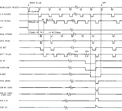
---~~---Figure 2-7 Write Cycle Timing Diagram
With the OVERFLOW fl ip-flop set I the next phase A pulse sets the BLAN K fl ip-flop
(5C4/4C4). The BLAN K fI ip-flop inhibits the phase A and phase B pulses for one drum clock period (lC8Y,5D2/4D2). Hence, a blank space (gap) separates the words written on the drum. The next phase B pulse resets the OVERFLOW
fI
ip-flop, and the next drum clock pulse resets the BLAN K. When the last word on the track is writtenj the BLANK flip-flop remains set; since there are no more clockpu I ses to reset B LAN K .
If the SCIDSA, the actions described above still occur; but the WRITE ENABLE flip-flop is not enabled, and no writing actually occurs on the drum.
As the OVERFLOW flip-flop is reset by the 13th phase B pulse, the trailing edge of the OVERFLOW signal (4C4/3C4) increments the sector count. When the BLAN K flip-flop is reset, the BLANKO signal (7C1/5C1) generates the TAKE WORD signal, which prepares the control circuits to
[image:27.612.77.524.76.447.2]write the next 13-bit word. (Refer to table 2-1 for the sequence of events following the TAKE WORD signal.) Note that the DF - - . DSB pulse generates the OB+ACT+DF - - . DSB pulse that prepares the WRITE DATA fl ip-flop to write the first bit of the next word. When the SC=DSA, the TAKE WORD signal (5B2/4B2) sets the RQ flip-flop to initiate a data break cycle to reload the DFB.
Writing continues until all 128 words of the addressed sector are written. The drum clock pulse that writes the parity bit of the 128th word of sector 7 (whether the NRZ writer is enabled or not) is the last drum clock pulse before the 300-fJsec gap. The DONE/START one-shot multivibrator
(5C2/4C2) reverts to the DONE state 3.4 fJsec after the last drum clock pulse. The DONE signal (5B6/4B6) sets the 4-state device to the FLAG state. The ACT signal (4C4/3C4) increments the DSA count, so that the next sector (or track if SA=7
8) is addressed in case continuous sector transfers are specified by the program.
After the FLAG state is set, the actions that follow depend on the computer. If the computer is programmed to write only one sector, the DRSC instruction (octal code 6622) generates the lOT 6622 pulse to sense the FLAG state (1 E1 OM, 5A7/ 4A7). When the FLAG state is 1, the I/O SKIP causes the computer to skip the next instruction and exit from the DRSC loop. The DRSE (code 6621) may then sense the drum control for errors. This is accomplished by the DRSE instruction, which generates the lOT 6621 pulse to sense the PEO ·DEO state (5A7/4A7). If no errors occur, the I/O SKIP signal causes the computer to skip the next instruction and exit from the drum write routine. If an error occurs, the program does not skip the next instruction which contains a JMP to an error check routine.
2.4.2 Writing Two Consecutive Sectors
When the computer is programmed to write more than one sector, instead of exiting from the write routine after one sector is written, the DRCN instruction causes writing to continue with the next sector. The DRCN instruction (refer to table 2-1) resets the PAR ERROR and DE flip-flops, generates TAKE WORD to prepare the control circuits to write the next word, and sets the 4-state device to TRA. With TRA set, the next index pulse sets the DONE/START multivibrator to START, which in turn sets the ACT state. The ACT enables the drum control circuits to write the next sector.
NOTE: Because the drum track selection circuits require 200 fJsec stabiliza-tion time, a new track must be specified during the first 100 fJsec of the 300-fJsec gap.
2.5 READ CYCLE
(A quick reference source table 2-2, Analysis of Instructions for the Read Cycle, is located at the end of this chapter.)
DAT A IN, and sets the READ/WRITE fl i p-flop to read. The program executes the DRTS instruction to load the DTA and DSA registers from the accumulator and, after a 200-f-Isec delay, sets the TRA state. The next index pulse sets the ACT state, which enables the drum control circuits to read the drum. Data read from the addressed drum track is strobed into the least significant bit of the DSB register, and the contents of the DSB are shifted. After twelve shifts the DSB contains the word read from the drum; then parity is checked. If a parity error occurs, the parity error flip-flop is set to indicate the error. If the SC=DSA, the DSB contents are transferred to the DFB, and the break request signal is sent to the computer. The computer enters a data break cycle to transfer the DFB contents into the memory location specified by the DCl register. The DCl contents then increment. Transfer continues in this manner until all 128 words of the addressed sector are read. After the last word on the drum track is encountered, the FLAG state is set to sign ify the completion of the sector transfer.
2.5.1 Detailed Discussion of Reading One Sector
The DRCR instruction (octal code 6603) applies the MB bits 3 through 8 and the lOP pulses to the device selector, to generate the lOT 6601 and 6602 pulses. (Table 2-2 shows the detailed signal flow of the DRCR instruction.) In brief, the DRCR instruction sets the IDLE state, clears the READ/WRITE flip-flop, and loads the DCl from the accumulator. The READ/WRITE flip-flop remains clear to signify the READ state. The READ signal causes the DATA IN signal (5B7/4B7) to be -3v, to signify a DATA I N direction to the data break circuits in the computer.
The DRTS instruction is then executed to load the DT A and DSA registers with the drum track and sector address of the forthcoming read cycle. As shown in table 2-2, the DRTS instruction prepares the control circuits to read the first word. Note that a 1 is inserted into DSB11 (by DSB IN! COND+400 nsec, 7C8) and the DSB register is cleared. After twelve shifts, the 1 inserted into DSB11 is in DSBF (7B2). Therefore, the DSBF 1 signal indicates that one word has been read from the drum. The read cycle timing diagram, figure 2-8, illustrates this condition.
After TRA is set, the control circuits wait for the index pulse. The index pulse sets the DONE/START one-shot multivibrator (5C2) to START, which in turn sets the 4-state device to ACT (SA6). The ACT signal (5C2) enables the drum clock pulses to produce phase A (OA), READ STROBE, and phase B (OB) pulses. As the drum rotates, the flux changes induce signals into the read heads. The addressed drum read head output is applied to the Type 1537 Sense Amplifier. The READ STROBE, occurring 0.25 f-Isec after the phase pulse, senses the sense amp!ifier (7C6) and produces a DATA READ pulse when a 1 is read from the drum; no pulse is produced when a 0 is read from the drum. The DATA READ pulse sets the DSBS flip-flop (7C8), and the shift pulse shifts the 1 from the DSBS into DSB11 as it shifts the DSB register.
DRUM CLOCK PULSES - - - - , ... - - - - , r - - -...
U..---.U,...--r
\--u
IGAP
+
U..----.U..----.U
o A PULSES
o B PULSES
ACT
READ STROBE
DATA READ
DS BS'
SHIFT PULSE
DS BF
OVERFLOW
BLANK
TAKE WORD
DSB INI COND
DSB INI COND
+ 400 nsec
DSB CLR
STEP SC
i II »)
0.3.usec---t - , --+l t4-70nsec , ::...
: U"-"-: -....,U
U""'--U
II !
({
IU :
U,...---"I)~}---iIL....;U
I I ~
---LJ----LJ---~'>l~)---~LJ~-T----~~ I
I
_ _ _ _ _ _ _ _ _ _ _ _ _ _ _ _ _ ~\)l~)---.
L-..--i-~
______________________
~\l~)---~---~~~J---~
L...-""";""---I
---~()~\---~LJ~---
I
Cl I
---~»)
LJ
_ _ _ _ _ _ _ _ _ _ _ _ _ _ _ _ _ _ _ _ _ _ ~!~I _ _ _ _ _ _ _ _ ~rl~
__________ _
) )
,
I
---_~(~(---~rl~---
))---~(~,---~~---
n
Figure 2-8 Read Cycle Timing Diagram
The shift pulse also resets the DSBS flip-flop. If the data bit read from the drum is 0, the DSBS fl ip-flop remains reset, and the shift pulse shifts a 0 into the DSB 11 fl ip-flop. Data transfers
continue in this manner until the original 1 bit that was in DSBS is shifted into DSBF. As the 1 is
shifted into the DSBF flip-flop, the DSBF1 signal sets the OVERFLOW flip-flop (7C4/5C4). The twelve
bits read from the drum are in the DSB register. The next phase B puise, enabled by READ and
OVER-FLOW, generates TAKE WORD and DSB INI COND (7C1/5B2). The DSB INI COND signal checks
parity {explained later} and prepares the circuits to read the next word from the drum. If SC=DSA, the TAKE WORD (7B2/5B2), transfers the DSB contents into the DFB and sets the RQ flip-flop (5A2/4A2).
The phase B pulse resets the OVERFLOW flip-flop, and OVERFLOWO (enabled by ACT I 4C3/4C3)
[image:30.615.110.527.81.460.2]When the RQ flip-flop is set, the word read from the drum is in the DFB. The RQ signal initiates a computer data break cycle to transfer the DFB contents into the memory location specified by the DCl (refer to table 2-2).
Data transfer continues in this manner until all words of the addressed sector are read. As the 300-jJsec gap is encountered, clock pulses cease to occur and the DONE/START multivibrator re-verts to the DONE state. The DONE signal sets the FLAG state. The trail ing edge of the ACT signal (4C7/4C7) advances the count of the DT A and DSA registers. With the FLAG state set, the program senses the FLAG state to exit from the read routine.
2.5.2 Reading Two Consecutive Sectors
If the program designates consecutive sector transfers, the DRCN instruction (refer to table 2-2) is executed to read the next sector. The DRCN instruction must occur during the first 100 jJsec of the 300-jJsec gap.
2.5.3 Parity Check
As a word is read from the drum, the DATA READ pulse complements the R PARITY fl ip-flop (7C5/5C5). The R PARITY is initially set. The DATA READ pulse occurs only when a 1 is read from the drum. Since odd parity is generated during the write cycle, the R PARITY fl ip-flop must be in a reset state after the 12-bit word, plus the parity bit, is read from the drum. If not, the DSB IN I CON D pulse sets the PE f/ ip-flop to indicate a parity error.
2.6 SPECIAL INSTRUCTIONS
2.6.1 DRCF Instruction
The DRCF (clear flag) instruction octal code 6611, generates the lOT 6611 pulse that resets the DE fl ip-flop (5B3/4B3), DT A (4C1/3B2-7), PE (7C4/5C4) and sets IDLE (5A4/4A4).
2.6.2 DREF Instruction
The DREF instruction loads the condition of the PE and DE into accumulator bits 0 and 1, respectively, to permit programmed evaluation of an error flag. The DREF instruction (octal code 6612) generates the lOT 6612 pulse. This pulse clears the AC (5C6/4C6) and generates a delayed 6612D pulse, which transfers DE to AC1 (5A4/4A4) and PE to ACO (7D5/5D5).
2.7 DATA ERROR AND PARITY ERROR
The data error is generated when the computer does not answer a break request before another break request is made. The break request signal sets the ER SYNC flip-flop (5A3/4A3). The T5D pulse,
occurring during a data break, resets the ER SYNC. If a data break does not occur, the ER SYNC remains set. The next RQ signal is enabled by ER SYNC to set the DE (data error) flip-flop. (Parity error detection is explained above.)
2.7.1 Sensing PE· DE
The state of PE· DE is sensed by the DRSE (lOT 6621). The lOT 6621 senses the PE· DE signal and causes a program skip if no error occurs (5A8/4A8).
2.7.2 Maintenance Switch Control of PE· DE
In the ON position, the MAINTENANCE ON/OFF switch (5D2) applies PEO. DEO to the gate (1 D9F, 5C3/4C3), which enables the phase A, phase B, and READ STROBE pulses. Detection of a data error or a parity error inhibits the clock signals so that all data transfer stops and the contents of a" registers can be observed to locate the cause of the error. In the OFF position the equipment functions normally and data errors or parity error can be detected via the error flag at the end of a
sector transfer.
2.8 DRUM TRACK SELECTION CIRCUITS
The drum track selection circuits are shown in engineering drawing BS-E-250-0-6
(BS-E-251-0-2). DTA bits 4 through 7 are appl ied to the Y selection circuits, and DTA bits 0 through 3 are appl ied to the X selection circuits. The addressed X selection circuit applies the read and write buses to a set of drum read/write heads. The addressed Y selection circuits provide a single return path for the group of read/write heads addressed by the X selection circuits. Hence, the DTA selects a single drum read/ write head by the coincidence of the X and Y selection lines. For example, when the DTA is clear
(DTA=OOOOOOOOO), the YO line and the XO line select the read/write head that is labeled "0-7." The 110-7" refers to the eight sectors written by that read/write head. Similarly, all other read/write heads are labeled with their track and sector address.
2.8.1 FIELD LOC KOUT Switches
FIELD LOC KOUT switches are provided for retaining data on certain fields, so as to be available for reading only. There are eight FIELD LOC KOUT switches (figure 4-1). Each switch prevents writing on four drum tracks. Switch 1 inhibits tracks 0 through
3i
switch 2 inhibits tracks 4 through 7i etc. Consequently I switch 8 inhibits tracks 34 through 37. The lockout is accomplished,as follows:
The DTA4 and DTA5 bits are applied to four decoders (4C5/3C5). Each decoder output LO
The WRITE signal is also an input to the decoders. The LOO through L03 signals are applied to the FIELD LOCKOUT switches as shown in 6D2 (2D2). When switch 1 is closed, LOO applies a negative potential to the XO selection to prevent writing on the addressed track O. Similarly, the other seven switches lock out their associated tracks.
2.9 POWER SUPPLY AND DISTRIBUTION (250 DRUM SYSTEM)
Primary power for the Type 250 Serial Drum is supplied by the computer. This power is supplied from the PDP-5 Power Control Type 832 as three lines: common, 115v via a contact of Kl and K3 (fast on-delayed off), and 115v via a contact of K2 (delayed on-fast off). Relays Kl, K2, and K3 are in the Power Control Type 832. The fast-on delayed-off input suppl ies ac for the drum motor, blower motor, and the + 10 and -15v power suppl ies in the Power Supply Type 779.
The common and delayed-on I ines supply the primary power for the remaining half (red, yellow, and green terminals) of the Power Supply Type 779. (Refer to engineering drawing PW-C-250-0-19.) Normally both channels of this dual supply are operated from a single source of primary power. In the 250 System, however, the supply is modified so that each channel (each transformer) is operated individually. (Refer to engineering drawing RS-779.) The outputs from the orange, yellow, and blue terminals are connected to the red (+ 10), black (ground), and blue (-15) color coded con-nectors, respectively, on each mounting panel of modules. The +15 and -15v of the remaining channel (the common terminal remains unconnected) are connected in series. The result of this connection is -30v (-15 -15
=
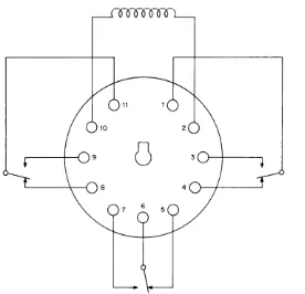
-30) provided for the NRZ Writer 4529, X Selection Modules 4530, Y Selection Modules 4531, and the isolation network shown at 7C6/7. This -30v potential is available after + 10 and -15v power is applied to the modules.A I2v dc relay is connected across the -15v terminal (refer to engineering drawing PW-C-250-0-19 and figure 2-9). The normally open contacts remove the -30vdc from the NRZ writer and X and Y selection circuits, and apply the I-mc clock from the PDP-5 to 1 C6F (5B4) to generate the DDC clear. After power is turned on the the -15v power supply rises to at least -12v, the relay energizes to remove the I-mc clock and apply -30v to the NRZ writer and the X and Y selection circuits.
Q
6
Figure 2-9 12v Relay Connections
2.10 POWER SUPPLY AND DISTRIBUTION (251 DRUM SYSTEM)
The 120 vac for the 251 Serial Drum is suppl ied by a 120-vac outlet. The ac is appl ied to the Power Control Type 832 in the 251 Drum System (refer to engineering drawing RS-832). Jumper wires connect terminals 1 to 3 and 4 to 5. Relay contacts in the 251 Drum 836 Power Control connect terminal 1 to 2, when the relay is energized; the relay is energized by -15v from the PDP-8 power supply (refer to engineering drawings PW-D-251-0-6 and RS-836). With the circuit breaker on and the REMOTE/LOCAL switch in the REMOTE position, ac power is suppl ied to relay contacts K1 and K2 when the -15v from the PDP-8 computer energizes the relay in the 836 Power Control. In the LOCAL position, ac power is appl ied to the Kl and K2 relays when the circuit breaker is on. The K2 contacts enable the fast-on delayed-off ac power. The Kl contacts apply ac to the time delay relay K3, which enables the delayed-on fast-off ac power.
[image:34.612.185.461.86.352.2]When power is initially applied to the 251 Drum System, a DDC CLEAR pulse is generated to normal ize control fl ip-flops in the drum control circu its. This is accompl ished by the Type 4401 Module (refer to engineering drawing 251-0-4, coordinates D2) supplying DDC CLEAR pulses to the system. An RC network delays the -15v to terminal V of the 4401 Module. Shortly after the applica-tion of power, terminal V is sufficiently negative to inhibit the clock pulses and the drum can function normally.
2.
11 DRUM MECHANICAL DESCRIPTION2.11. 1 Drum Head Mounting Description
The full complement of magnetic heads is mounted on the drum in a series of blocks, with a line of heads in each block, and the gaps coplanar at one surface, as shown in the simplified mechanical diagram, figure 2-10. The flat surface serves as the pad or slider of a hydrodynamic bearing, using the boundary layer of air clinging to the rotating drum as a lubricating or self-pressurizing medium. A single thin strip of spring steel connects each magnetic head/bearing pad to the drum frame. The spring steel reed serves as a combined motion pivot, loading spring, and mounting canti lever.
HYDRODYNAMIC AIR BEARING PAD, WITH INTE.GRAL MAGNETIC HEADS
Figure 2-10 Drum Head Mounting
MOUNTING BAR ON DRUM FRAME
The action of this simple mechanical system for placing the magnetic head pad in close proximity to the drum surface, when the drum is at operating speed, is illustrated in figure 2-11.
Figure 2-11 Operating Position of the Head Pad
2.11 .2 Mec han i ca
I
ActuatorThe mechanical actuator moves the head into close proximity ot the drum surface when the drum is up to speed. As the drum comes to speed, a centrifugal switch, mounted on the motor end, closes and sets a delay relay (red cap). The relay energizes in 1.5 min, and sets another time-delay relay (yellow cap), which supplies actuating power to the linear motor actuator for 6 sec. After the linear motor pulls in the heads, a holding coil, which is energized from rectified ac, holds in the heads. The 1 .5-min delay permits the drum to reach full speed prior to actuation. The 6-sec interval must not be exceeded, because the linear motor has a very short duty cycle and can burn out if left energized. A circuit breaker, thermally actuated by the linear motor current, provides further pro-tection for the motor.
Normal shut down of drum power or any power failure instantly raises the heads. Motor burnout, while not anticipated, results in speed loss, so that the centrifugal switch opens and raises the heads. A fuse mount, located under the right front corner of the cabinet, contains a switch for actuating the heads. The drum centrifugal switch must be closed to operate this switch. If holding coil fails to hold at the end of the pull-in cycle, the manual switch must be opened and closed to re-start the cye! e .
2.12 ANALYSIS OF INSTRUCTIONS
[image:36.617.214.391.99.204.2]